NJD35N04G NPN Darlington Power Transistor
This high voltage power Darlington has been specifically designed for inductive applications such as Electronic Ignition, Switching Regulators and Motor Control.
Features http://onsemi.com
• Exceptional Safe Operating Area • High VCE; High Current Gain • These are Pb−Free Devices
Benefits
• Reliable Performance at Higher Powers • Designed for Inductive Loads • Very Low Current Requirements
Applications
DARLINGTON POWER TRANSISTORS 4 AMPERES 350 VOLTS 45 WATTS
MARKING DIAGRAM
4 12
• • • • •
Internal Combustion Engine Ignition Control Switching Regulators Motor Controls Light Ballast Photo Flash
3
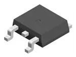
DPAK CASE 369C STYLE 1
YWW NJD 35N04G
MAXIMUM RATINGS
Rating Collector−Emitter Sustaining Voltage Collector−Base Breakdown Voltage Collector−Emitter Breakdown Voltage Emitter−Base Voltage Collector Current Base Current Total Power Dissipation @ TC = 25°C Derate above 25°C Operating and Storage Junction Temperature Range Continuous Peak Symbol VCEO VCBO VCES VEBO IC ICM IB PD TJ, Tstg Value 350 700 700 5.0 4.0 8.0 0.5 45 0.36 − 65 to +150 Unit Vdc Vdc Vdc Vdc Adc Adc W W/°C °C
Y = Year WW = Work Week NJD35N04 = Device Code G = Pb−Free Device
ORDERING INFORMATION
Device NJD35N04G NJD35N04T4G Package DPAK (Pb−Free) DPAK (Pb−Free) Shipping† 75 Units / Rail 2500/Tape & Reel
Stresses exceeding Maximum Ratings may damage the device. Maximum Ratings are stress ratings only. Functional operation above the Recommended Operating Conditions is not implied. Extended exposure to stresses above the Recommended Operating Conditions may affect device reliability.
†For information on tape and reel specifications, including part orientation and tape sizes, please refer to our Tape and Reel Packaging Specification Brochure, BRD8011/D.
THERMAL CHARACTERISTICS
Characteristic Thermal Resistance Junction−to−Case Junction−to−Ambient Symbol RqJC RqJA Value 2.78 71.4 Unit °C/W
© Semiconductor Components Industries, LLC, 2010
July, 2010 − Rev. 2
1
Publication Order Number: NJD35N04/D
�NJD35N04G
ELECTRICAL CHARACTERISTICS (TC = 25°C unless otherwise noted)
Characteristic OFF CHARACTERISTICS Collector−Emitter Sustaining Voltage (IC = 10 mA, L = 10 mH) Collector Cutoff Current (VCE = 500 V) (IB = 0) (VCE = 500 V, TC = 125°C) Collector Cutoff Current (VCE = 350 V) (IB = 0) (VCE = 300 V, TC = 125°C) Emitter Cutoff Current (VBE = 5.0 Vdc) ON CHARACTERISTICS Collector−Emitter Saturation Voltage (IC = 2.0 A, IB = 20 mA) (IC = 2.0 A, IB = 20 mA 125°C) Base−Emitter Saturation Voltage (IC = 2.0 A, IB = 20 mA) (IC = 2.0 A, IB = 20 mA 125°C) Base−Emitter On Voltage (IC = 2.0 A, VCE = 2.0 V) (IC = 2.0 A, VCE = 2.0 V 125°C) DC Current Gain (IC = 2.0 A, VCE = 2.0 V) (IC = 4.0 A, VCE = 2.0 Vdc) DYNAMIC CHARACTERISTICS Current−Gain − Bandwidth Product (IC = 2.0 A, VCE = 10 V, f = 1.0 MHz) Output Capacitance (VCB = 10 V, IE = 0, f = 0.1 MHz) SWITCHING CHARACTERISTICS VCC = 12 V, Vclamp = 250 V, L = 4 mH IC = 2 A, IB1 = 20 mA, IB2 = −20 mA ts tf − − 18 0.8 − − mSec fT Cob 90 − − MHz VCE(sat) − − VCEO(sus) ICES ICEO IEBO 350 − − Vdc Symbol Min Typ Max Unit
− − − − −
− − − − −
50 250 50 250 5.0
mAdc
mAdc
mAdc
1.5
Vdc
VBE(sat)
−
−
2.0
Vdc
VBE(on)
−
−
2.0
Vdc
hFE
2000 300
−
−
−
−
−
−
60
−
pF
C B E 2 KW
Figure 1. Darlington Circuit Schematic
http://onsemi.com
2
�NJD35N04G
TYPICAL CHARACTERISTICS
50 PD, POWER DISSIPATION (W) 45 35 30 25 20 15 10 5.0 0 10 10 30 50 70 90 110 130 150 170 T, TEMPERATURE (°C) 0.1 TC hFE, DC CURRENT GAIN 40 10,000 125°C 1000 25°C
100
VCE = 2 V 1.0 IC, COLLECTOR CURRENT (AMPS) 10
Figure 2. Power Derating
4.0 VCE(sat), COLLECTOR−EMITTER SATURATION VOLTAGE (V) 3.5 3.0 2.5 2.0 1.5 1.0 0.5 0 25°C 125°C 0.1 1.0 IC, COLLECTOR CURRENT (AMPS) Ic/Ib = 100 2.4 2.0 1.6
Figure 3. DC Current Gain
VBE(sat), BASE−EMITTER SATURATION VOLTAGE (V)
25°C 1.2 0.8 0.4 0 125°C Ic/Ib = 100 0.1 1.0 IC, COLLECTOR CURRENT (AMPS) 10
10
Figure 4. Collector−Emitter Saturation Voltage
Figure 5. Base−Emitter Saturation Voltage
VBE(on), BASE−EMITTER VOLTAGE (V)
2.0 IC, COLLECTOR CURRENT (A)
10 10 mS 100 mS 1 mS 300 mS
1.6 25°C
DC 1.0
1.2
0.1
0.8 125°C 0.4 0.1 1.0 IC, COLLECTOR CURRENT (AMPS) 10 VCE = 2 V
0.01
10
100 VCE, COLLECTOR−EMITTER VOLTAGE (V)
1000
Figure 6. Base−Emitter Voltage
Figure 7. Forward Bias Safe Operating Area (FBSOA)
http://onsemi.com
3
�NJD35N04G
PACKAGE DIMENSIONS
DPAK CASE 369C−01 ISSUE D
C A B c2
NOTES: 1. DIMENSIONING AND TOLERANCING PER ASME Y14.5M, 1994. 2. CONTROLLING DIMENSION: INCHES. 3. THERMAL PAD CONTOUR OPTIONAL WITHIN DIMENSIONS b3, L3 and Z. 4. DIMENSIONS D AND E DO NOT INCLUDE MOLD FLASH, PROTRUSIONS, OR BURRS. MOLD FLASH, PROTRUSIONS, OR GATE BURRS SHALL NOT EXCEED 0.006 INCHES PER SIDE. 5. DIMENSIONS D AND E ARE DETERMINED AT THE OUTERMOST EXTREMES OF THE PLASTIC BODY. 6. DATUMS A AND B ARE DETERMINED AT DATUM PLANE H. DIM A A1 b b2 b3 c c2 D E e H L L1 L2 L3 L4 Z INCHES MIN MAX 0.086 0.094 0.000 0.005 0.025 0.035 0.030 0.045 0.180 0.215 0.018 0.024 0.018 0.024 0.235 0.245 0.250 0.265 0.090 BSC 0.370 0.410 0.055 0.070 0.108 REF 0.020 BSC 0.035 0.050 −−− 0.040 0.155 −−− MILLIMETERS MIN MAX 2.18 2.38 0.00 0.13 0.63 0.89 0.76 1.14 4.57 5.46 0.46 0.61 0.46 0.61 5.97 6.22 6.35 6.73 2.29 BSC 9.40 10.41 1.40 1.78 2.74 REF 0.51 BSC 0.89 1.27 −−− 1.01 3.93 −−−
E b3 L3
1 4
A
D
2 3
Z
DETAIL A
H
L4
b2 e
b 0.005 (0.13)
M
c C L2
GAUGE PLANE
H C L L1 DETAIL A
SEATING PLANE
A1
ROTATED 90 CW 5
SOLDERING FOOTPRINT*
6.20 0.244 3.0 0.118
STYLE 1: PIN 1. BASE 2. COLLECTOR 3. EMITTER 4. COLLECTOR
2.58 0.101
5.80 0.228
1.6 0.063
6.172 0.243
SCALE 3:1
mm inches
*For additional information on our Pb−Free strategy and soldering details, please download the ON Semiconductor Soldering and Mounting Techniques Reference Manual, SOLDERRM/D.
ON Semiconductor and are registered trademarks of Semiconductor Components Industries, LLC (SCILLC). SCILLC reserves the right to make changes without further notice to any products herein. SCILLC makes no warranty, representation or guarantee regarding the suitability of its products for any particular purpose, nor does SCILLC assume any liability arising out of the application or use of any product or circuit, and specifically disclaims any and all liability, including without limitation special, consequential or incidental damages. “Typical” parameters which may be provided in SCILLC data sheets and/or specifications can and do vary in different applications and actual performance may vary over time. All operating parameters, including “Typicals” must be validated for each customer application by customer’s technical experts. SCILLC does not convey any license under its patent rights nor the rights of others. SCILLC products are not designed, intended, or authorized for use as components in systems intended for surgical implant into the body, or other applications intended to support or sustain life, or for any other application in which the failure of the SCILLC product could create a situation where personal injury or death may occur. Should Buyer purchase or use SCILLC products for any such unintended or unauthorized application, Buyer shall indemnify and hold SCILLC and its officers, employees, subsidiaries, affiliates, and distributors harmless against all claims, costs, damages, and expenses, and reasonable attorney fees arising out of, directly or indirectly, any claim of personal injury or death associated with such unintended or unauthorized use, even if such claim alleges that SCILLC was negligent regarding the design or manufacture of the part. SCILLC is an Equal Opportunity/Affirmative Action Employer. This literature is subject to all applicable copyright laws and is not for resale in any manner.
PUBLICATION ORDERING INFORMATION
LITERATURE FULFILLMENT: Literature Distribution Center for ON Semiconductor P.O. Box 5163, Denver, Colorado 80217 USA Phone: 303−675−2175 or 800−344−3860 Toll Free USA/Canada Fax: 303−675−2176 or 800−344−3867 Toll Free USA/Canada Email: orderlit@onsemi.com N. American Technical Support: 800−282−9855 Toll Free USA/Canada Europe, Middle East and Africa Technical Support: Phone: 421 33 790 2910 Japan Customer Focus Center Phone: 81−3−5773−3850 ON Semiconductor Website: www.onsemi.com Order Literature: http://www.onsemi.com/orderlit For additional information, please contact your local Sales Representative
http://onsemi.com
4
NJD35N04/D
�


 工商网监
湘ICP备2023018690号
工商网监
湘ICP备2023018690号
