NL3HS644
2:1 MIPI D-PHY (1.5 Gbps)
4-Data Lane Switch
The NL3HS644 is a 4−data lane MIPI, D−PHY switch. This
single−pole double−throw (SPDT) switch is optimized for switching
between 2 high−speed or low−power MIPI sources. The NL3HS644 is
designed for MIPI specifications and allows connection to a CSI or
DSI module.
www.onsemi.com
Features
•
•
•
•
•
•
•
•
•
•
•
•
•
•
•
Operating Supply: VCC = 1.65 V to 4.5 V
Switch Signal Range: 0 to VCC
Signal Types: MIPI, D−PHY
ON−Resistance:
RON = 8 W (Typ) HS MIPI
RON = 7.9 W (Typ) LP MIPI
ON−Resistance Mismatch:
DRON = 0.09 W (Typ) HS MIPI
DRON = 0.17 W (Typ) LP MIPI
ON Resistance Flatness:
RON_FLAT = 0.03 W (Typ) HS MIPI
RON_FLAT = 0.46 W (Typ) LP MIPI
Supply Current: ICC = 55 mA (Max)
Hi−Z Supply Current: ICCZ = 5 mA (Max)
Off−Isolation: OIRR = −27 dB (Typ)
Crosstalk: XTALK = −28 dB (Typ)
Bandwidth: BW = 1,050 MHz (Typ)
Channel to Channel Skew: tSK = 63 ps (Typ)
ON Capacitance: CON = 12.6 pF
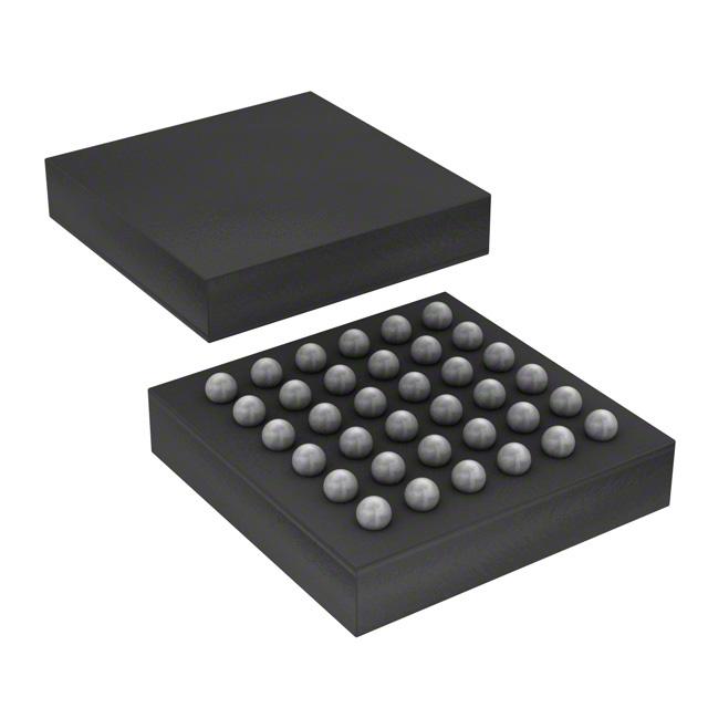
36−Ball WLCSP Package, 2.36 mm x 2.36 mm
This device is Pb−Free, Halogen−Free/BFR−Free and are
RoHS−Compliant
WLCSP36
FC SUFFIX
CASE 567LR
MARKING DIAGRAM
XXXXXX
AWLYWW
G
XXXXXX = Device Code
A
= Assembly Location
WL = Wafer Lot
Y
= Year
WW = Work Week
G
= Pb−Free Package
ORDERING INFORMATION
See detailed ordering, marking and shipping information in the
package dimensions section on page 8 of this data sheet.
Figure 1. Typical Application – Mobile Phone
© Semiconductor Components Industries, LLC, 2015
November, 2015 − Rev. 2
1
Publication Order Number:
NL3HS644/D
�NL3HS644
FUNCTION TABLE
OE
SEL
FUNCTION
L
L
CLKP = CLKAP, CLKN = CLKAN, DnP = DAnP, DnN = DAnN
L
H
CLKP = CLKBP, CLKN = CLKBN, DnP = DBnP, DnN = DBnN
H
X
CLKAP/CLKAN, CLKBP/CLKBN, DAnP/DAnN, DBnP/DBnN Ports at High Impedance
Figure 2. Block Diagram
Figure 3. Pinout (Top Through View)
PIN ASSIGNMENT
Pin Name
Ball
Description
CLKP / CLKN
A2 / A1
Common Clock Path
D1P / D1N
B2 / B1
Common Data Path 1
D2P / D2N
C2 / C1
Common Data Path 2
D3P / D3N
D2 / D1
Common Data Path 3
D4P / D4N
E2 / E1
Common Data Path 4
CLKAP / CLKAN
A3 / B3
A−Side Clock Path
DA1P / DA1N
A4 / B4
A−Side Data Path 1
DA2P / DA2N
A5 / A6
A−Side Data Path 2
DA3P / DA3N
B5 / B6
A−Side Data Path 3
DA4P / DA4N
C5 / C6
A−Side Data Path 4
CLKBP / CLKBN
D6 / D5
B−Side Clock Path
DB1P / DB1N
E6 / E5
B−Side Data Path 1
DB2P / DB2N
F6 / F5
B−Side Data Path 2
DB3P / DB3N
E4 / F4
B−Side Data Path 3
DB4P / DB4N
E3 / F3
B−Side Data Path 4
SEL
F2
Control Pin
OE
F1
Output Enable
VCC
C4
Power
GND
D3
Ground
NC
C3 / D4
SEL = L:
CLKP = CLKAP, CLKN = CLKAN, DnP = DAnP, DnN = DAnN
SEL = H:
CLKP = CLKBP, CLKN = CLKBN, DnP = DBnP, DnN = DBnN
No Connect
www.onsemi.com
2
�NL3HS644
MAXIMUM RATINGS
Symbol
Rating
Value
Unit
−0.5 to +5.5
V
−0.5 to VCC + 0.5
V
−0.5 to +5.5
V
VCC
Positive DC Supply Voltage
VIS
Analog Input Voltage
VIN
Digital Control Input Voltage (SEL or OE)
IOS
Switch Output Current
50
mA
IIOK
Switch Input/Output Diode Current
−50
mA
IIK
Control Input Diode Current
±50
mA
Ts
Storage Temperature
−65 to +150
°C
Stresses exceeding those listed in the Maximum Ratings table may damage the device. If any of these limits are exceeded, device functionality
should not be assumed, damage may occur and reliability may be affected.
RECOMMENDED OPERATING CONDITIONS
Symbol
Parameter
VCC
Positive DC Supply Voltage
VIS
Switch Input / Output Voltage
VIN
Min
Max
Unit
1.65
4.5
V
V
HS Mode
0.1
0.3
LP Mode
0
1.2
GND
VCC
Digital Control Input Voltage (SEL or OE) (Note 1)
V
1. Control input must be held High or Low. It must not float.
DC ELECTRICAL CHARACTERISTICS
Voltages referenced to GND. All typical values are at TA = 25°C unless otherwise specified.
TA = −40°C to +85°C
Symbol
Parameter
Condition
VCC (V)
Min
Typ
Max
Unit
−1.2
V
DIGITAL CONTROL SECTION (SEL or OE)
VIK
Clamp Diode Voltage
VIH
Input Voltage High
1.65 – 4.5
VIL
Input Voltage Low
1.65 – 4.5
0.4
V
IIN
Input Leakage Current
VIN = 0 V to VCC
1.65 – 4.5
±100
nA
Switch ON Resistance
ION = −10 mA, OE =
1.8
9
12
W
for HS MIPI Applications
0 V, SEL = VCC or 0 V,
2.5
8
9
(Note 2)
CLKA, CLKB, DBn or
3.6
8
9
DAn = 0.1, 0.2, 0.3 V
4.5
8
9
Switch ON Resistance
ION = −10 mA, OE =
1.8
9.5
12
for LP MIPI Applications
0 V, SEL = VCC or 0 V,
2.5
8.5
10
(Note 2)
CLKA, CLKB, DBn or
3.6
7.9
9
9
IIN = −18 mA
2.8
1.0
V
SWITCHES
RON_MIPI_
HS
RON_MIPI_LP
DRON_
MIPI_HS
DAn = 0, 0.6, 1.2 V
4.5
7.6
ON Resistance Matching
ION = −10 mA, OE =
1.8
0.02
Between HS MIPI
0 V, SEL = VCC or 0 V,
2.5
0.09
Channels (Note 3)
CLKA, CLKB, DBn or
3.6
0.09
DAn = 0.1, 0.2, 0.3 V
4.5
0.08
W
W
2. Measured by the voltage drop between A and B pins at the indicated current through the switch. ON resistance is determined by the lower
of the voltage on the two (A or B ports).
3. Guaranteed by characterization.
www.onsemi.com
3
�NL3HS644
DC ELECTRICAL CHARACTERISTICS
Voltages referenced to GND. All typical values are at TA = 25°C unless otherwise specified.
TA = −40°C to +85°C
Symbol
Parameter
Condition
VCC (V)
Min
Typ
Max
Unit
SWITCHES
DRON_
MIPI_LP
RON_FLAT_
MIPI_HS
RON_FLAT_
MIPI_LP
ON Resistance Matching
ION = −10 mA, OE =
1.8
0.17
Between LP MIPI
0 V, SEL = VCC or 0 V,
2.5
0.12
Channels (Note 3)
CLKA, CLKB, DBn or
3.6
0.17
DAn = 0, 0.6, 1.2 V
4.5
0.09
ON Resistance Flatness
ION = −10 mA, OE =
1.8
0.23
for HS MIPI Channels
0 V, SEL = VCC or 0 V,
2.5
0.11
(Note 3)
CLKA, CLKB, DBn or
3.6
0.03
DAn = 0.1, 0.2, 0.3 V
4.5
0.02
ON Resistance Flatness
ION = −10 mA, OE =
1.8
2.09
for LP MIPI Channels
0 V, SEL = VCC or 0 V,
2.5
1.19
(Note 3)
CLKA, CLKB, DBn or
3.6
0.46
DAn = 0, 0.6, 1.2 V
4.5
0.08
W
W
W
OFF Leakage Current
(CLKAn, DAn, CLKBn, DBn)
CLKn, Dn = 0.3 V, VCC – 0.3 V,
CLKAn, DAn, or CLKBn; DBn =
VCC – 0.3 V, 0.3 V or Floating;
OE = 0 V
1.65 – 4.5
±100
nA
ON Leakage Current of
Common Ports (CLKn, Dn)
CLKn, Dn = 0.3 V, VCC – 0.3 V,
CLKAn, DAn, or CLKBn; DBn =
VCC – 0.3 V, 0.3 V or Floating;
OE = 0 V
1.65 – 4.5
±100
nA
VIK
Clamp Diode Voltage
IIN = −18 mA
2.8
−1.2
V
IOZ
Off−State Leakage Current
0 v CLKn, Dn, CLKAn, CLKBn,
DAn, DBn v 3.6 V; OE = High
4.5
±100
nA
INO(OFF),
INC(OFF)
IA(ON)
SUPPLY CURRENTS
ICCZ
Quiescent Hi−Z Supply
Current
VIN = 0 or VCC, IOUT = 0
4.5
0.5
mA
ICC
Quiescent Supply Current
VIN = 0 or VCC, IOUT = 0
2.5 to 4.5
55
mA
1.8
30
4.5
4.0
ICCT
Increase in ICC Current per
VSEL, V(OE) = 1.65 V
Control Voltage and VCC
2.5
0.1
mA
1.0
2. Measured by the voltage drop between A and B pins at the indicated current through the switch. ON resistance is determined by the lower
of the voltage on the two (A or B ports).
3. Guaranteed by characterization.
www.onsemi.com
4
�NL3HS644
AC ELECTRICAL CHARACTERISTICS All typical values are for VCC = 3.3 V at TA = 25°C unless otherwise specified.
TA = −40°C to +85°C
Condition
VCC (V)
Min
Initialization Time
RL = 50 W, CL = 5 pF, VIS = 1.2 V
2.5 to 4.5
100
VCC to Output (Notes 4, 5)
Figure 4
1.8
150
Enable Turn−On Time
RL = 50 W, CL = 5 pF, VIS = 1.2 V
OE to Output
Figure 5
Disable Turn−Off Time
RL = 50 W, CL = 5 pF, VIS = 1.2 V
OE to Output
Figure 5
Turn−On Time
RL = 50 W, CL = 5 pF, VIS = 1.2 V
SEL to Output
Figure 5
Turn−Off Time
RL = 50 W, CL = 5 pF, VIS = 1.2 V
SEL to Output
Figure 5
tBBM
Break−Before−Make Time
RL = 50 W, CL = 5 pF, VIS = 1.2 V
Figure 6
OIRR
Off−Isolation for MIPI (Note 4)
RL = 50 W, f = 750 MHz, OE =
VCC, VIS = −1 dBm (200 mVPP)
XTALK
Crosstalk for MIPI (Note 4)
RL = 50 W, f = 750 MHz,
VIS = −1 dBm (200 mVPP)
BW
−3 dB Bandwidth (Note 4)
RL = 50 W, CL = 0 pF
3.0
Differential Data Rate
Inter−Operability Data Rate
3.0
Parameter
Symbol
tINIT
tEN
tDIS
tON
tOFF
SDD21
Typ
Max
ms
2.5 to 4.5
120
200
1.8
250
500
2.5 to 4.5
25
50
1.8
50
90
2.5 to 4.5
50
100
1.8
75
125
2.5 to 4.5
50
200
1.8
200
325
10
Unit
ms
ns
ns
ns
50
ns
1.65 to 4.5
−27
dB
1.65 to 4.5
−28
dB
1050
MHz
1.5
Gbps
900
4. Guaranteed by characterization.
5. Wait time required after VCC power−up to operating level before data access is valid.
HIGH SPEED−RELATED AC ELECTRICAL CHARACTERISTICS
TA = −40°C to +85°C
Symbol
Parameter
Condition
tSK(O)
Channel−to−Channel
Single−Ended Skew (Note 6)
TDR−Based Method
(VIS = 0.2 VPP, CL = CON) Figure 7
tSK(P)
Skew of Opposite Transitions
of the Same Output (Note 6)
TDR−Based Method
(VIS = 0.2 VPP, CL = CON) Figure 8
Typ
Max
Unit
3.3
63
67
ps
3.3
17
31
ps
VCC (V)
Min
6. Guaranteed by characterization.
CAPACITANCE
TA = −40°C to +85°C
Condition
Typ
Max
Symbol
Parameter
CIN
Control Pin Input Capacitance
VCC = 0 V, f = 1 MHz
3.3
14.9
pF
CON
Out ON Capacitance
VCC = 3.3 V, OE = 0 V, f = 1 MHz
3.3
12.6
pF
COFF
Out OFF Capacitance
VCC = 3.3 V, OE = 3.3 V, f = 1 MHz
3.3
7.4
pF
www.onsemi.com
5
VCC (V)
Min
Unit
�NL3HS644
Timing Diagrams
Operating Level
VCC
tINIT
Transactions Not Valid
Transactions Valid
Figure 4. tINIT, Initialization Time
tF =
2.5 ns
tR =
2.5 ns
90%
SEL /
OE
50%
VCC
VCC
90%
50 %
10%
SEL
10%
GND
GND
VOH
tOFF /
tDIS
VA and V B
OUTPUT
INPUT
10 % x V OH
tON /
tEN
VOL
GND
VOH
90 % x V OH
VO
90 % x V O
OUTPUT
VOL
tBBM
Figure 5. tEN, tDIS, tON, tOFF Times
0.2 VPP
90 % x V O
OUTPUT
P−Ch/
N−Ch
N−Ch/
P−Ch
Midpoint
N−Ch/
P−Ch
tSK(O)
Figure 6. tBBM, Break−Before−Make Time
P−Ch/N−Ch
Same Channel
Midpoint
P−Ch/
N−Ch
0.2 VPP
Midpoint
tSK(P)
tSK(O)
Figure 7. tSK(O), Channel−to−Channel
Single−Ended
Figure 8. tSK(P), Same Channel Opposite
Transitions
www.onsemi.com
6
�NL3HS644
Eye Diagrams
Figure 9. D−PHY HS 1.5 Gbps with Eye Mask
Figure 10. D−PHY LP 80 Mbps with Eye Mask
www.onsemi.com
7
�NL3HS644
DEVICE ORDERING INFORMATION
Device Code
Package Type
Tape & Reel Size†
NL3HS644FCTAG
3HS644
36−ball WLCSP
(Pb−Free)
3000 / Tape & Reel
NL3HS644BFCTAG
(Backside Coated)
HS644B
36−ball WLCSP
(Pb−Free)
3000 / Tape & Reel
Device Order Number
†For information on tape and reel specifications, including part orientation and tape sizes, please refer to our Tape and Reel Packaging
Specifications Brochure, BRD8011/D.
PACKAGE DIMENSIONS
PIN A1
REFERENCE
ÈÈ
ÈÈ
WLCSP36 2.34x2.34
CASE 567LR
ISSUE B
E
A
NOTES:
1. DIMENSIONING AND TOLERANCING PER
ASME Y14.5M, 1994.
2. CONTROLLING DIMENSION: MILLIMETERS.
3. COPLANARITY APPLIES TO SPHERICAL
CROWNS OF SOLDER BALLS.
B
A2
BACKSIDE
COATING
D
A
DIM
A
A1
A2
b
D
E
e
0.10 C
2X
0.10 C
2X
TOP VIEW
DETAIL A
A
DETAIL A
OPTIONAL
CONSTRUCTION
A1
0.10 C
MILLIMETERS
MIN
MAX
−−−
0.54
0.17
0.23
0.00
0.027
0.24
0.30
2.34 BSC
2.34 BSC
0.40 BSC
RECOMMENDED
SOLDERING FOOTPRINT*
0.08 C
C
SIDE VIEW
NOTE 3
SEATING
PLANE
A1
PACKAGE
OUTLINE
e/2
36X
0.05 C A B
0.03 C
e
b
F
e
E
D
0.40
PITCH
e/2
36X
0.40
PITCH
C
B
A
0.20
DIMENSIONS: MILLIMETERS
*For additional information on our Pb−Free strategy and soldering
details, please download the ON Semiconductor Soldering and
Mounting Techniques Reference Manual, SOLDERRM/D.
1 2 3 4 5 6
BOTTOM VIEW
ON Semiconductor and the
are registered trademarks of Semiconductor Components Industries, LLC (SCILLC) or its subsidiaries in the United States and/or other countries.
SCILLC owns the rights to a number of patents, trademarks, copyrights, trade secrets, and other intellectual property. A listing of SCILLC’s product/patent coverage may be accessed
at www.onsemi.com/site/pdf/Patent−Marking.pdf. SCILLC reserves the right to make changes without further notice to any products herein. SCILLC makes no warranty, representation
or guarantee regarding the suitability of its products for any particular purpose, nor does SCILLC assume any liability arising out of the application or use of any product or circuit, and
specifically disclaims any and all liability, including without limitation special, consequential or incidental damages. “Typical” parameters which may be provided in SCILLC data sheets
and/or specifications can and do vary in different applications and actual performance may vary over time. All operating parameters, including “Typicals” must be validated for each
customer application by customer’s technical experts. SCILLC does not convey any license under its patent rights nor the rights of others. SCILLC products are not designed, intended,
or authorized for use as components in systems intended for surgical implant into the body, or other applications intended to support or sustain life, or for any other application in which
the failure of the SCILLC product could create a situation where personal injury or death may occur. Should Buyer purchase or use SCILLC products for any such unintended or
unauthorized application, Buyer shall indemnify and hold SCILLC and its officers, employees, subsidiaries, affiliates, and distributors harmless against all claims, costs, damages, and
expenses, and reasonable attorney fees arising out of, directly or indirectly, any claim of personal injury or death associated with such unintended or unauthorized use, even if such claim
alleges that SCILLC was negligent regarding the design or manufacture of the part. SCILLC is an Equal Opportunity/Affirmative Action Employer. This literature is subject to all applicable
copyright laws and is not for resale in any manner.
PUBLICATION ORDERING INFORMATION
LITERATURE FULFILLMENT:
Literature Distribution Center for ON Semiconductor
19521 E. 32nd Pkwy, Aurora, Colorado 80011 USA
Phone: 303−675−2175 or 800−344−3860 Toll Free USA/Canada
Fax: 303−675−2176 or 800−344−3867 Toll Free USA/Canada
Email: orderlit@onsemi.com
N. American Technical Support: 800−282−9855 Toll Free
USA/Canada
Europe, Middle East and Africa Technical Support:
Phone: 421 33 790 2910
Japan Customer Focus Center
Phone: 81−3−5817−1050
www.onsemi.com
8
ON Semiconductor Website: www.onsemi.com
Order Literature: http://www.onsemi.com/orderlit
For additional information, please contact your local
Sales Representative
NL3HS644/D
�


 工商网监
湘ICP备2023018690号
工商网监
湘ICP备2023018690号
