NLAS4052
Analog Multiplexer/
Demultiplexer
Double–Pole, 4–Position
Plus Common Off
The NLAS4052 is an improved version of the MC14052 and
MC74HC4052 fabricated in sub–micron Silicon Gate CMOS
technology for lower RDS(on) resistance and improved linearity with
low current. This device may be operated either with a single supply or
dual supply up to ±3 V to pass a 6 VPP signal without coupling
capacitors.
When operating in single supply mode, it is only necessary to tie
VEE, pin 7 to ground. For dual supply operation, VEE is tied to a
negative voltage, not to exceed maximum ratings.
http://onsemi.com
MARKING DIAGRAMS
16
SO–16
D SUFFIX
CASE 751B
• Improved RDS(on) Specifications
• Pin for Pin Replacement for MAX4052 and MAX4052A
•
•
9
NLAS4052
AWLYWW
1
8
16
– One Half the Resistance Operating at 5.0 Volts
Single or Dual Supply Operation
– Single 2.5–5 Volt Operation, or Dual ±3 Volt Operation
– With VCC of 3.0 to 3.3 V, Device Can Interface with 1.8 V Logic,
– No Translators Needed
– Address and Inhibit pins are Logic is Over–Voltage Tolerant and –
– May Be Driven Up +6 V Regardless of VCC
Address and Inhibit pins are Standard TTL Compatible
– Greatly Improved Noise Margin Over MAX4052 and MAX4052A
Improved Linearity Over Standard HC4052 Devices
•
• Popular SOIC, and Space Saving TSSOP, and QSOP 16 Pin
TSSOP–16
DT SUFFIX
CASE 948F
NLAS
4052
ALYW
1
8
16
QSOP–16
QS SUFFIX
CASE 492
A
WL, L
Y
WW, W
Packages
9
9
NLAS
4052
ALYW
1
8
= Assembly Location
= Wafer Lot
= Year
= Work Week
ORDERING INFORMATION
Device
Package
Shipping
SO–16
2500 Units/Reel
NLAS4052DTR2
TSSOP–16
2500 Units/Reel
NLAS4052QSR
QSOP–16
2500 Units/Reel
NLAS4052DR2
Semiconductor Components Industries, LLC, 2002
June, 2002 – Rev. 1
1
Publication Order Number:
NLAS4052/D
�NLAS4052
VCC
16
1
NO1A NO2A COMA NO0A NO3A ADDB ADDA
15
2
14
3
13
12
4
5
11
10
6
7
NO0B NO1B COMB NO3B NO2B Inhibit VEE
9
NO0B
8
GND
NO1B
NO1A
COMB
NO2A
NO3B
COMA
NO2B
NO0A
NO3A
Figure 1. Pin Connection
(Top View)
ADDB
ADDA
LOGIC
Figure 2. Logic Diagram
TRUTH TABLE
Address
Inhibit
B
A
ON SWITCHES*
1
X
don’t care
X
don’t care
All switches open
0
0
0
COMA–NO0A,
COMB–NO0B
0
0
1
COMA–NO1A,
COMB–NO1B
0
1
0
COMA–NO2A,
COMB–NO2B
0
1
1
COMA–NO3A,
COMB–NO3B
*NO and COM pins are identical and interchangeable. Either may be
considered an input or output; signals pass equally well in either direction.
http://onsemi.com
2
Inhibit
�NLAS4052
ÎÎÎÎÎÎÎÎÎÎÎÎÎÎÎÎÎÎÎÎÎÎÎÎÎÎÎÎÎÎÎÎÎ
ÎÎÎÎÎ
ÎÎÎÎÎÎÎÎÎÎÎÎÎÎÎÎÎÎÎÎÎ
ÎÎÎÎÎÎÎ
ÎÎÎ
ÎÎÎÎÎÎÎÎÎÎÎÎÎÎÎÎÎÎÎÎÎÎÎÎÎÎÎÎÎÎÎÎÎ
ÎÎÎÎÎ
ÎÎÎÎÎÎÎÎÎÎÎÎÎÎÎÎÎÎÎÎÎ
ÎÎÎÎÎÎÎ
ÎÎÎ
ÎÎÎÎÎ
ÎÎÎÎÎÎÎÎÎÎÎÎÎÎÎÎÎÎÎÎÎ
ÎÎÎÎÎÎÎ
ÎÎÎ
ÎÎÎÎÎ
ÎÎÎÎÎÎÎÎÎÎÎÎÎÎÎÎÎÎÎÎÎ
ÎÎÎÎÎÎÎ
ÎÎÎ
ÎÎÎÎÎ
ÎÎÎÎÎÎÎÎÎÎÎÎÎÎÎÎÎÎÎÎÎ
ÎÎÎÎÎÎÎ
ÎÎÎ
ÎÎÎÎÎ
ÎÎÎÎÎÎÎÎÎÎÎÎÎÎÎÎÎÎÎÎÎ
ÎÎÎÎÎÎÎ
ÎÎÎ
ÎÎÎÎÎ
ÎÎÎÎÎÎÎÎÎÎÎÎÎÎÎÎÎÎÎÎÎ
ÎÎÎÎÎÎÎ
ÎÎÎ
ÎÎÎÎÎ
ÎÎÎÎÎÎÎÎÎÎÎÎÎÎÎÎÎÎÎÎÎ
ÎÎÎÎÎÎÎ
ÎÎÎ
ÎÎÎÎÎ
ÎÎÎÎÎÎÎÎÎÎÎÎÎÎÎÎÎÎÎÎÎ
ÎÎÎÎÎÎÎ
ÎÎÎ
ÎÎÎÎÎ
ÎÎÎÎÎÎÎÎÎÎÎÎÎÎÎÎÎÎÎÎÎ
ÎÎÎÎÎÎÎ
ÎÎÎ
ÎÎÎÎÎ
ÎÎÎÎÎÎÎÎÎÎÎÎÎÎÎÎÎÎÎÎÎ
ÎÎÎÎÎÎÎ
ÎÎÎ
ÎÎÎÎÎ
ÎÎÎÎÎÎÎÎÎÎÎÎÎÎÎÎÎÎÎÎÎ
ÎÎÎÎÎÎÎ
ÎÎÎ
ÎÎÎÎÎ
ÎÎÎÎÎÎÎÎÎÎÎÎÎÎÎÎÎÎÎÎÎ
ÎÎÎÎÎÎÎ
ÎÎÎ
ÎÎÎÎÎ
ÎÎÎÎÎÎÎÎÎÎÎÎÎÎÎÎÎÎÎÎÎ
ÎÎÎÎÎÎÎ
ÎÎÎ
ÎÎÎÎÎ
ÎÎÎÎÎÎÎÎÎÎÎÎÎÎÎÎÎÎÎÎÎ
ÎÎÎÎÎÎÎ
ÎÎÎ
ÎÎÎÎÎ
ÎÎÎÎÎÎÎÎÎÎÎÎÎÎÎÎÎÎÎÎÎ
ÎÎÎÎÎÎÎ
ÎÎÎ
ÎÎÎÎÎ
ÎÎÎÎÎÎÎÎÎÎÎÎÎÎÎÎÎÎÎÎÎ
ÎÎÎÎÎÎÎ
ÎÎÎ
ÎÎÎÎÎ
ÎÎÎÎÎÎÎÎÎÎÎÎÎÎÎÎÎÎÎÎÎ
ÎÎÎÎÎÎÎ
ÎÎÎ
ÎÎÎÎÎ
ÎÎÎÎÎÎÎÎÎÎÎÎÎÎÎÎÎÎÎÎÎ
ÎÎÎÎÎÎÎ
ÎÎÎ
ÎÎÎÎÎ
ÎÎÎÎÎÎÎÎÎÎÎÎÎÎÎÎÎÎÎÎÎ
ÎÎÎÎÎÎÎ
ÎÎÎ
MAXIMUM RATINGS (Note 1)
Symbol
Parameter
Value
Unit
VEE
Negative DC Supply Voltage
(Referenced to GND)
–7.0 to �0.5
V
VCC
Positive DC Supply Voltage (Note 2)
(Referenced to GND)
(Referenced to VEE)
–0.5 to �7.0
–0.5 to �7.0
V
VIS
Analog Input Voltage
VEE –0.5 to VCC �0.5
V
VIN
Digital Input Voltage
–0.5 to 7.0
V
I
DC Current, Into or Out of Any Pin
�50
mA
TSTG
Storage Temperature Range
–65 to �150
°C
TL
Lead Temperature, 1 mm from Case for 10 Seconds
260
°C
TJ
Junction Temperature under Bias
�150
°C
�JA
Thermal Resistance
SOIC
TSSOP
QSOP
143
164
164
°C/W
PD
Power Dissipation in Still Air,
SOIC
TSSOP
QSOP
500
450
450
mW
MSL
Moisture Sensitivity
FR
Flammability Rating
VESD
ESD Withstand Voltage
Human Body Model (Note 3)
Machine Model (Note 4)
Charged Device Model (Note 5)
�2000
�200
�1000
V
ILATCH–UP
Latch–Up Performance
Above VCC and Below GND at 125°C (Note 6)
�300
mA
(Referenced to GND)
Level 1
Oxygen Index: 30% – 35%
UL 94 V–0 @ 0.125 in
1. Absolute maximum continuous ratings are those values beyond which damage to the device may occur. Extended exposure to these
conditions or conditions beyond those indicated may adversely affect device reliability. Functional operation under absolute maximum–rated
conditions is not implied.
2. The absolute value of VCC �|VEE| ≤ 7.0.
3. Tested to EIA/JESD22–A114–A.
4. Tested to EIA/JESD22–A115–A.
5. Tested to JESD22–C101–A.
6. Tested to EIA/JESD78.
RECOMMENDED OPERATING CONDITIONS
ÎÎÎÎ
ÎÎÎÎÎÎÎÎÎÎÎÎÎÎÎÎÎÎÎÎÎÎ
ÎÎÎÎ
ÎÎÎÎ
ÎÎÎ
ÎÎÎÎ
ÎÎÎÎÎÎÎÎÎÎÎÎÎÎÎÎÎÎÎÎÎÎ
ÎÎÎÎ
ÎÎÎÎ
ÎÎÎ
ÎÎÎÎ
ÎÎÎÎÎÎÎÎÎÎÎÎÎÎÎÎÎÎÎÎÎÎ
ÎÎÎÎ
ÎÎÎÎ
ÎÎÎ
ÎÎÎÎ
ÎÎÎÎÎÎÎÎÎÎÎÎÎÎÎÎÎÎÎÎÎÎ
ÎÎÎÎ
ÎÎÎÎ
ÎÎÎ
ÎÎÎÎ
ÎÎÎÎÎÎÎÎÎÎÎÎÎÎÎÎÎÎÎÎÎÎ
ÎÎÎÎ
ÎÎÎÎ
ÎÎÎ
ÎÎÎÎ
ÎÎÎÎÎÎÎÎÎÎÎÎÎÎÎÎÎÎÎÎÎÎ
ÎÎÎÎ
ÎÎÎÎ
ÎÎÎ
ÎÎÎÎ
ÎÎÎÎÎÎÎÎÎÎÎÎÎÎÎÎÎÎÎÎÎÎ
ÎÎÎÎ
ÎÎÎÎ
ÎÎÎ
ÎÎÎÎ
ÎÎÎÎÎÎÎÎÎÎÎÎÎÎÎÎÎÎÎÎÎÎ
ÎÎÎÎ
ÎÎÎÎ
ÎÎÎ
Symbol
Parameter
Min
Max
Unit
VEE
Negative DC Supply Voltage
(Referenced to GND)
–5.5
GND
V
VCC
Positive DC Supply Voltage
(Referenced to GND)
(Referenced to VEE)
2.5
2.5
5.5
6.6
V
VIS
Analog Input Voltage
VEE
VCC
V
VIN
Digital Input Voltage
TA
Operating Temperature Range, All Package Types
tr, tf
Input Rise/Fall Time
(Channel Select or Enable Inputs)
(Note 7) (Referenced to GND)
VCC = 3.0 V � 0.3 V
VCC = 5.0 V � 0.5 V
0
5.5
V
–55
125
°C
0
0
100
20
ns/V
7. Unused digital inputs may not be left open. All digital inputs must be tied to a high–logic voltage level or a low–logic input voltage level.
http://onsemi.com
3
�NLAS4052
DC CHARACTERISTICS – Digital Section (Voltages Referenced to GND)
Guaranteed Max Limit
Symbol
Parameter
Condition
VCC
–55 to 25�C
很抱歉,暂时无法提供与“NLAS4052QSR”相匹配的价格&库存,您可以联系我们找货
免费人工找货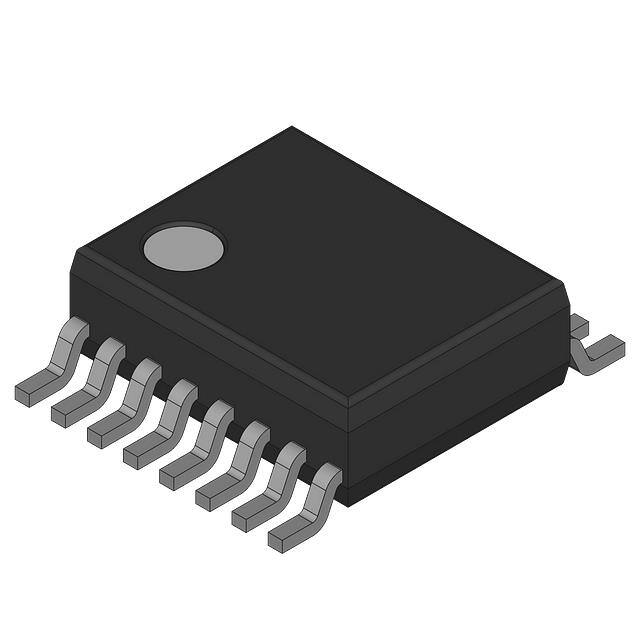


 工商网监
湘ICP备2023018690号
工商网监
湘ICP备2023018690号
