NLX1G74
Single D Flip-Flop
The NLX1G74 is a high performance, full function edge−triggered
D Flip−Flop in ultra−small footprint. The NLX1G74 input structures
provide protection when voltages up to 7.0 V are applied, regardless of
the supply voltage.
http://onsemi.com
Features
•
•
•
•
•
•
•
•
•
Extremely High Speed: tPD = 2.6 ns (typical) at VCC = 5.0 V
Designed for 1.65 V to 5.5 V VCC Operation
MARKING
DIAGRAM
Low Power Dissipation: ICC = 1 mA (Max) at TA = 25°C
1
24 mA Balanced Output Sink and Source Capability at VCC = 3.0 V
1
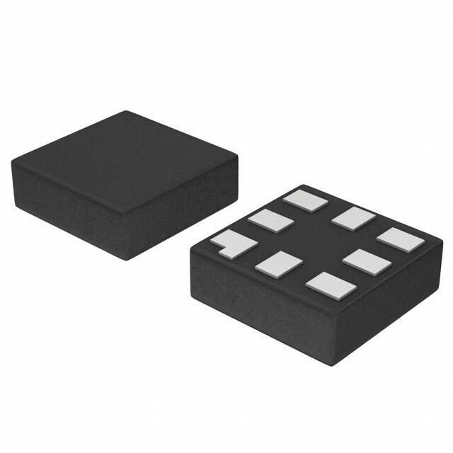
UQFN8
MU SUFFIX
CASE 523AN
Balanced Propagation Delays
Overvoltage Tolerant (OVT) Input Pins
AA MG
G
AA = Device Code
M = Date Code*
G = Pb−Free Package
Ultra Small Package
NLV Prefix for Automotive and Other Applications Requiring
Unique Site and Control Change Requirements; AEC−Q100
Qualified and PPAP Capable
This is a Pb−Free Device
8
(Note: Microdot may be in either location)
PINOUT DIAGRAM
CP
7
D
6
Q
5
TRUTH TABLE
Inputs
VCC 8
Outputs
PR
CLR
CP
D
Q
Q
Operating Mode
L
H
L
H
L
L
X
X
X
X
X
X
H
L
H
L
H
H
Asynchronous Set
Asynchronous Clear
Undetermined
H
H
H
H
↑
↑
h
l
H
L
L
H
Load and Read Register
H
H
↑
X
NC
NC
Hold
4 GND
1
PR
2
3
CLR Q
LOGIC DIAGRAM
PR
H
h
= High Voltage Level
= High Voltage Level One Setup Time Prior to the Low−to−High
Clock Transition
L
= Low Voltage Level
l
= Low Voltage Level One Setup Time Prior to the Low−to−High
Clock Transition
NC
= No Change
X
= High or Low Voltage Level and Transitions are Acceptable
↑
= Low−to−High Transition
↑
= Not a Low−to−High Transition
For ICC reasons, DO NOT FLOAT Inputs
1
D
6
3
Q
CP
7
5
Q
2
CLR
VCC = 8, GND = 4
ORDERING INFORMATION
See detailed ordering and shipping information in the package
dimensions section on page 2 of this data sheet.
© Semiconductor Components Industries, LLC, 2013
September, 2013 − Rev. 1
1
Publication Order Number:
NLX1G74/D
�NLX1G74
MAXIMUM RATINGS
Symbol
Value
Unit
DC Supply Voltage
−0.5 to +7.0
V
VI
DC Input Voltage
−0.5 to +7.0
V
VO
DC Output Voltage − Output in High or Low State (Note 1)
−0.5 to VCC +0.5
V
VCC
Parameter
IIK
DC Input Diode Current
VI < GND
−50
mA
IOK
DC Output Diode Current
VO < GND
−50
mA
IO
DC Output Sink Current
±50
mA
ICC
DC Supply Current Per Supply Pin
±100
mA
IGND
DC Ground Current Per Ground Pin
±100
mA
TSTG
Storage Temperature Range
−65 to +150
°C
°C
TL
Lead Temperature, 1 mm from Case for 10 Seconds
260
TJ
Junction Temperature Under Bias
+150
°C
qJA
Thermal Resistance (Note 2)
250
°C/W
PD
Power Dissipation in Still Air at 85°C
250
mW
MSL
Moisture Sensitivity
FR
Flammability Rating
Oxygen Index: 28 to 34
ESD Withstand Voltage
Human Body Model (Note 3)
Machine Model (Note 4)
Charged Device Model (Note 5)
VESD
Level 1
UL 94 V−0 @ 0.125 in
>2000
>200
N/A
V
Stresses exceeding Maximum Ratings may damage the device. Maximum Ratings are stress ratings only. Functional operation above the
Recommended Operating Conditions is not implied. Extended exposure to stresses above the Recommended Operating Conditions may affect
device reliability.
1. IO absolute maximum rating must be observed.
2. Measured with minimum pad spacing on an FR4 board, using 10 mm X 1 inch, 2 ounce copper trace with no air flow.
3. Tested to EIA/JESD22−A114−A.
4. Tested to EIA/JESD22−A115−A.
5. Tested to JESD22−C101−A.
RECOMMENDED OPERATING CONDITIONS
Symbol
VCC
Parameter
Supply Voltage
Operating
Data Retention Only
Min
Max
Unit
1.65
1.5
5.5
5.5
V
VI
Input Voltage
(Note 6)
0
5.5
V
VO
Output Voltage
(HIGH or LOW State)
0
VCC
V
TA
Operating Free−Air Temperature
−40
+85
°C
Dt/DV
Input Transition Rise or Fall Rate
0
0
0
20
10
5.0
ns/V
VCC = 2.5 V ±0.2 V
VCC = 3.0 V ±0.3 V
VCC = 5.0 V ±0.5 V
6. Unused inputs may not be left open. All inputs must be tied to a high−logic voltage level or a low−logic input voltage level.
ORDERING INFORMATION
Package
Shipping†
NLX1G74MUTCG
UQFN8
(Pb−Free)
3000 / Tape & Reel
NLVX1G74MUTCG*
UQFN8
(Pb−Free)
3000 / Tape & Reel
Device
†For information on tape and reel specifications, including part orientation and tape sizes, please refer to our Tape and Reel Packaging
Specifications Brochure, BRD8011/D.
*NLV Prefix for Automotive and Other Applications Requiring Unique Site and Control Change Requirements; AEC−Q100 Qualified and PPAP
Capable.
http://onsemi.com
2
�NLX1G74
DC ELECTRICAL CHARACTERISTICS
TA = 25_C
VCC
Symbol
Parameter
VIH
High−Level Input Voltage
VIL
Condition
Low−Level Input Voltage
(V)
Min
1.65
0.75 VCC
0.75 VCC
2.3 to 5.5
0.7 VCC
0.7 VCC
Max
Min
Max
1.65
0.25 VCC
0.25 VCC
0.3 VCC
0.3 VCC
High−Level Output Voltage
VIN = VIL or VIL
IOH = 100 mA
IOH = −3 mA
IOH = −8 mA
IOH = −12 mA
IOH = −16 mA
IOH = −24 mA
IOH = −32 mA
1.65 to 5.5
1.65
2.3
2.7
3.0
3.0
4.5
VOL
Low−Level Output Voltage
VIN = VIH
IOL = 100 mA
IOL = 3 mA
IOL = 8 mA
IOL = 12 mA
IOL = 16 mA
IOL = 24 mA
IOL = 32 mA
1.65 to 5.5
1.65
2.3
2.7
3.0
3.0
4.5
VCC − 0.1
1.29
1.9
2.2
2.4
2.3
3.8
VCC
1.52
2.1
2.4
2.7
2.5
4.0
0.008
0.10
0.12
0.15
0.19
0.30
0.30
Unit
V
2.3 to 5.5
VOH
IIN
Typ
*40_C v TA v 85_C
VCC − 0.1
1.29
1.9
2.2
2.4
2.3
3.8
V
V
0.1
0.24
0.3
0.4
0.4
0.55
0.55
0.1
0.24
0.3
0.4
0.4
0.55
0.55
V
Input Leakage Current
VIN = VCC or GND
5.5
$0.1
$1.0
mA
IOFF
Power off Input
Leakage Current
5.5V or VIN = GND
0
1.0
10
mA
ICC
Quiescent Supply Current
VIN = VCC or GND
5.5
1.0
10
mA
http://onsemi.com
3
�NLX1G74
ÎÎÎÎÎÎÎÎÎÎÎÎÎÎÎÎÎÎÎÎÎÎÎÎÎÎÎÎÎÎÎÎÎ
ÎÎÎÎÎÎÎÎÎÎÎÎÎÎÎÎÎÎÎÎÎÎÎÎÎÎÎÎÎÎÎÎÎ
ÎÎÎÎ
ÎÎÎÎÎÎÎÎÎÎÎÎÎÎÎÎÎÎÎÎÎÎÎÎÎÎÎÎÎÎÎÎÎÎÎ
ÎÎÎÎÎÎÎÎÎÎÎÎÎÎÎÎÎÎÎÎÎÎÎÎÎÎÎ
ÎÎÎÎÎÎÎ
ÎÎÎÎÎ
ÎÎÎÎÎÎÎÎÎ
ÎÎÎÎÎÎ
ÎÎÎ
ÎÎÎÎÎÎÎÎÎÎÎÎÎÎÎÎÎÎÎÎÎÎÎÎÎÎÎÎÎÎÎÎÎ
ÎÎÎÎÎÎ
ÎÎÎÎÎÎÎ
ÎÎ
ÎÎÎÎÎÎÎÎÎÎÎÎÎÎÎÎÎÎÎÎÎÎÎÎÎÎÎÎÎÎÎÎÎÎÎÎÎÎÎÎÎÎ
ÎÎÎÎ
ÎÎÎÎÎÎÎ
ÎÎÎÎÎÎÎÎ
ÎÎÎ
ÎÎÎÎÎ
ÎÎÎ
ÎÎÎ
ÎÎÎ
ÎÎÎ
ÎÎÎ
ÎÎÎÎÎÎÎÎÎÎÎÎÎÎÎÎÎÎÎÎÎÎÎÎÎÎÎÎÎÎÎÎÎ
ÎÎÎÎÎÎ
ÎÎÎÎÎÎÎÎÎ
ÎÎÎÎÎÎÎÎÎÎÎÎÎÎÎÎÎÎÎÎÎÎÎÎÎÎÎÎÎÎÎÎÎÎÎÎÎÎÎÎÎÎ
ÎÎÎÎ
ÎÎÎÎÎÎÎÎ
ÎÎÎÎÎÎÎÎÎÎÎÎÎÎÎ
ÎÎÎÎÎÎÎÎÎÎÎ
ÎÎÎÎÎÎÎÎÎÎÎÎ
ÎÎÎÎÎÎÎÎÎÎÎ
ÎÎÎ
ÎÎÎÎÎ
ÎÎÎ
ÎÎÎ
ÎÎÎ
ÎÎÎ
ÎÎÎ
ÎÎÎÎ
ÎÎÎÎÎÎÎ
ÎÎÎ
ÎÎÎÎÎ
ÎÎÎÎÎÎÎÎ
ÎÎÎ
ÎÎÎ
ÎÎÎ
ÎÎÎ
ÎÎÎ
ÎÎÎÎÎÎÎÎÎÎÎÎÎÎÎÎÎÎÎÎÎÎÎÎÎÎÎÎÎÎÎÎÎÎÎÎÎÎÎÎÎÎ
ÎÎÎÎÎÎÎÎÎÎÎÎÎÎÎÎÎÎÎÎÎÎÎÎÎÎÎÎÎÎÎÎÎÎÎÎÎÎÎÎÎÎ
ÎÎÎÎÎÎÎÎÎÎÎÎÎÎÎÎÎÎÎÎÎÎÎÎÎÎÎÎÎÎÎÎÎÎÎÎÎÎÎÎÎÎ
ÎÎÎÎÎÎÎÎÎÎÎÎÎÎÎÎÎÎÎÎÎÎÎÎÎÎÎÎÎÎÎÎÎÎÎÎÎÎÎÎÎÎ
ÎÎÎÎÎÎÎÎÎÎÎÎÎÎÎÎÎÎÎÎÎÎÎÎÎÎÎÎÎÎÎÎÎÎÎÎÎÎÎÎÎÎ
ÎÎÎÎÎÎÎÎÎÎÎÎÎÎÎÎÎÎÎÎÎÎÎÎÎÎÎÎÎÎÎÎÎÎÎÎÎÎÎÎÎÎ
ÎÎÎÎÎÎÎÎÎÎÎÎÎÎÎÎÎÎÎÎÎÎÎÎÎÎÎÎÎÎÎÎÎÎÎÎÎÎÎÎÎÎ
ÎÎÎÎÎÎÎÎÎÎÎÎÎÎÎÎÎÎÎÎÎÎÎÎÎÎÎÎÎÎÎÎÎ
ÎÎÎ
Î
ÎÎ
Î
ÎÎÎ
ÎÎ
ÎÎÎ
ÎÎÎÎ
ÎÎÎÎÎÎÎ
ÎÎÎ
ÎÎÎÎÎ
ÎÎÎÎÎÎÎÎ
ÎÎÎ
ÎÎÎ
ÎÎÎ
ÎÎÎ
ÎÎÎ
ÎÎÎÎÎÎÎÎÎÎÎÎÎÎÎÎÎÎÎÎÎÎÎÎÎÎÎÎÎÎÎÎÎÎÎÎÎÎÎÎÎÎ
ÎÎÎ
ÎÎÎÎÎÎÎÎÎÎÎÎÎÎÎÎÎÎÎÎÎÎÎÎÎÎÎÎÎÎÎÎÎ
ÎÎÎÎÎÎ
ÎÎÎÎÎÎÎ
ÎÎ
ÎÎÎÎ
ÎÎÎÎÎÎÎ
ÎÎÎÎÎÎÎÎ
ÎÎÎ
ÎÎÎÎÎ
ÎÎÎ
ÎÎÎ
ÎÎÎ
ÎÎÎ
ÎÎÎ
ÎÎÎÎÎÎÎÎÎÎÎÎÎÎÎÎÎÎÎÎÎÎÎÎÎÎÎÎÎÎÎÎÎÎÎÎÎÎÎÎÎÎ
ÎÎÎÎÎÎÎÎÎÎÎÎÎÎÎÎÎÎÎÎÎÎÎÎÎÎÎÎÎÎÎÎÎ
ÎÎÎÎÎÎ
ÎÎÎÎÎÎÎÎÎ
ÎÎÎÎÎÎÎÎÎÎÎÎÎÎÎÎÎÎÎÎÎÎÎÎÎÎÎÎÎÎÎÎÎÎÎÎÎÎÎÎÎÎ
ÎÎÎÎ
ÎÎÎÎÎÎÎ
ÎÎÎÎÎÎÎÎ
ÎÎÎ
ÎÎÎÎÎ
ÎÎÎ
ÎÎÎ
ÎÎÎ
ÎÎÎ
ÎÎÎ
ÎÎÎÎÎÎÎÎÎÎÎÎÎÎÎÎÎÎÎÎÎÎÎÎÎÎÎÎÎÎÎÎÎ
ÎÎÎÎÎÎ
ÎÎÎÎÎÎÎÎÎ
ÎÎÎÎ
ÎÎÎÎÎÎÎ
ÎÎÎ
ÎÎÎÎÎ
ÎÎÎÎÎÎÎÎ
ÎÎÎ
ÎÎÎ
ÎÎÎ
ÎÎÎ
ÎÎÎ
ÎÎÎÎÎÎÎÎÎÎÎÎÎÎÎÎÎÎÎÎÎÎÎÎÎÎÎÎÎÎÎÎÎÎÎÎÎÎÎÎÎÎ
ÎÎÎ
ÎÎÎÎ
ÎÎÎÎÎÎÎ
ÎÎÎÎÎ
ÎÎÎÎÎÎÎÎ
ÎÎÎ
ÎÎÎ
Î
ÎÎÎ
ÎÎ
Î
ÎÎÎ
ÎÎ
ÎÎÎ
Î
ÎÎ
ÎÎÎÎÎÎÎÎÎÎÎÎÎÎÎÎÎÎÎÎÎÎÎÎÎÎÎÎÎÎÎÎÎÎÎÎÎÎÎÎÎÎ
ÎÎÎÎÎÎÎÎÎÎÎÎÎÎÎÎÎÎÎÎÎÎÎÎÎÎÎÎÎÎÎÎÎÎÎÎÎÎÎÎÎÎ
ÎÎÎÎÎÎÎÎÎÎÎÎÎÎÎÎÎÎÎÎÎÎÎÎÎÎÎÎÎÎÎÎÎ
ÎÎÎÎÎ
ÎÎÎÎÎÎÎÎÎ
ÎÎÎÎÎÎÎÎÎÎÎÎÎÎÎÎÎÎÎÎÎÎÎÎÎÎÎÎÎÎÎ
ÎÎÎÎÎÎÎÎÎÎÎÎ
AC ELECTRICAL CHARACTERISTICS (Input tr = tf = 3.0 ns)
TA = 25°C
Parameter
Maximum Clock
Frequency
(50% Duty Cycle)
(Waveform 1)
VCC (V)
Test Conditions
CL = 15 pF
RD = 1 MW
S1 = Open
Min
Typ
TA = −40 to 85°C
Min
Max
Unit
MHz
1.8 ± 0.15
75
75
2.5 ± 0.2
150
150
3.3 ± 0.3
200
200
5.0 ± 0.5
250
250
CL = 50 pF,
3.3 ± 0.3
175
175
RD = 500 W, S1 = Open
5.0 ± 0.5
200
200
tPLH,
Propagation Delay,
CL = 15 pF
ns
1.8 ± 0.15
2.5
6.5
12.5
2.5
13
tPHL
CP to Q or Q
RD = 1 MW
2.5 ± 0.2
1.5
3.8
7.5
1.5
8.0
(Waveform 1)
S1 = Open
3.3 ± 0.3
1.0
2.8
6.5
1.0
7.0
5.0 ± 0.5
0.8
2.2
4.5
0.8
5.0
CL = 50 pF,
3.3 ± 0.3
1.0
3.4
7.0
1.0
7.5
RD = 500 W, S1 = Open
5.0 ± 0.5
1.0
2.6
5.0
1.0
5.5
tPLH,
Propagation Delay,
CL = 15 pF
ns
1.8 ± 0.15
2.5
6.5
14
2.5
14.5
tPHL
PR or CLR to Q or Q
RD = 1 MW
2.5 ± 0.2
1.5
3.8
9.0
1.5
9.5
(Waveform 2)
S1 = Open
3.3 ± 0.3
1.0
2.8
6.5
1.0
7.0
5.0 ± 0.5
0.8
2.2
5.0
0.8
5.5
CL = 50 pF,
3.3 ± 0.3
1.0
3.4
7.0
1.0
7.5
RD = 500 W, S1 = Open
5.0 ± 0.5
1.0
2.6
5.0
1.0
5.5
tS
Setup Time, D to CP
CL = 15 pF
ns
1.8 ± 0.15
6.5
6.5
(Waveform 1)
RD = 1 MW
2.5 ± 0.2
3.5
3.5
S1 = Open
3.3 ± 0.3
2.0
2.0
5.0 ± 0.5
1.5
1.5
CL = 50 pF,
3.3 ± 0.3
2.0
2.0
RD = 500 W, S1 = Open
5.0 ± 0.5
1.5
1.5
tH
Hold Time, D to CP
CL = 15 pF
ns
1.8 ± 0.15
0.5
0.5
(Waveform 1)
RD = 1 MW
2.5 ± 0.2
0.5
0.5
S1 = Open
3.3 ± 0.3
0.5
0.5
5.0 ± 0.5
0.5
0.5
CL = 50 pF,
3.3 ± 0.3
0.5
0.5
RD = 500 W, S1 = Open
5.0 ± 0.5
0.5
0.5
tW
Pulse Width,
CL = 15 pF
ns
1.8 ± 0.15
6.0
6.0
CP, CLR, PR
RD = 1 MW
2.5 ± 0.2
4.0
4.0
(Waveform 3)
S1 = Open
3.3 ± 0.3
3.0
3.0
5.0 ± 0.5
2.0
2.0
CL = 50 pF,
3.3 ± 0.3
3.0
3.0
RD = 500 W, S1 = Open
5.0 ± 0.5
2.0
2.0
tREC
Recover Time
CL = 15 pF
MHz
1.8 ± 0.15
8.0
8.0
PR; CLR to CP
RD = 1 MW
2.5 ± 0.2
4.5
4.5
(Waveform 3)
S1 = Open
3.3 ± 0.3
3.0
3.0
5.0 ± 0.5
3.0
3.0
CL = 50 pF,
3.3 ± 0.3
3.0
3.0
RD = 500 W, S1 = Open
5.0 ± 0.5
3.0
3.0
7. CPD is defined as the value of the internal equivalent capacitance which is calculated from the operating current consumption without load.
Average operating current can be obtained by the equation: ICC(OPR) = CPD � VCC � fin + ICC / 2 (per flip−flop). CPD is used to determine the
no−load dynamic power consumption; PD = CPD � VCC2 � fin + ICC � VCC.
Symbol
fMAX
Max
CAPACITANCE (Note 8)
Symbol
Condition
Typical
Unit
Input Capacitance
VCC = 5.5 V
7.0
pF
COUT
Output Capacitance
VCC = 5.5 V
7.0
pF
CPD
Power Dissipation Capacitance (Note 9)
Frequency = 10 MHz
VCC = 3.3 V
VCC = 5.0 V
16
21
pF
CIN
Parameter
8. TA = +25°C, f = 1 MHz
9. CPD is defined as the value of the internal equivalent capacitance which is derived from dynamic operating current consumption (ICCD) at
no output loading and operating at 50% duty cycle. (See Figure 1) CPD is related to ICCD dynamic operating current by the expression:
ICCD = CPD � VCC � fin + ICC(static).
http://onsemi.com
4
�NLX1G74
Vcc
D
50%
0V
th
ts
Vcc
tw
CP
50%
0V
fmax
tPLH, tPHL
VOH
Q,
Q
50%
VOL
WAVEFORM 1 − PROPAGATION DELAYS, SETUP AND HOLD TIMES
tR = tF = 3.0 ns, 10% to 90%; f = 1 MHz; tW = 500 ns
Vcc
PR
50%
0V
Vcc
CLR
50%
0V
tPLH
tPHL
Q
50%
50%
VOL
VOH
tPLH
Q
50%
tPHL
50%
WAVEFORM 2 − PROPAGATION DELAYS
tR = tF = 3.0 ns, 10% to 90%; f = 1 MHz; tW = 500 ns
PR, CLR
Vcc
tw
50%
0V
trec
Vcc
50%
CP
tw
0V
WAVEFORM 3 − RECOVERY TIME
tR = tF = 3.0 ns from 10% to 90%; f = 1 MHz; tw = 500 ns
Output Reg: VOL ≤ 0.8 V, VOH ≥ 2.0 V
Figure 1. AC Waveforms
VCC
PULSE
GENERATOR
DUT
RT
CL
Figure 2. Test Circuit
http://onsemi.com
5
RL
�MECHANICAL CASE OUTLINE
PACKAGE DIMENSIONS
UQFN8, 1.6x1.6, 0.5P
CASE 523AN−01
ISSUE O
8
1
SCALE 4:1
A
B
D
PIN ONE
REFERENCE
2X
0.10 C
ÉÉ
ÉÉ
ÇÇÇ
ÇÇÇ
ÉÉÉ
EXPOSED Cu
E
A1
DATE 26 NOV 2008
NOTES:
1. DIMENSIONING AND TOLERANCING PER
ASME Y14.5M, 1994.
2. CONTROLLING DIMENSION: MILLIMETERS.
3. DIMENSION b APPLIES TO PLATED TERMINAL
AND IS MEASURED BETWEEN 0.15 AND
0.30 mm FROM THE TERMINAL TIP.
MOLD CMPD
A3
DETAIL B
DIM
A
A1
A3
b
D
E
e
L
L1
L3
OPTIONAL
CONSTRUCTION
2X
0.10 C
TOP VIEW
L1
(A3)
DETAIL B
L3
A
0.05 C
b
0.05 C
SIDE VIEW
(0.10)
C
A1
SEATING
PLANE
(0.15)
DETAIL A
OPTIONAL
CONSTRUCTION
GENERIC
MARKING DIAGRAM*
1
8X
8X
L3
L
XX MG
e
5
3
1
XX = Specific Device Code
M = Date Code
G
= Pb−Free Package
7
8
DETAIL A
MILLIMETERS
MIN
MAX
0.45
0.60
0.00
0.05
0.13 REF
0.15
0.25
1.60 BSC
1.60 BSC
0.50 BSC
0.35
0.45
−−−
0.15
0.25
0.35
8X
b
*This information is generic. Please refer
to device data sheet for actual part
marking.
Pb−Free indicator, “G” or microdot “ G”,
may or may not be present.
0.10 C A B
BOTTOM VIEW
0.05 C
NOTE 3
SOLDERING FOOTPRINT*
1.70
0.50
PITCH
1
0.35
7X
0.25
1.70
8X
0.53
DIMENSIONS: MILLIMETERS
*For additional information on our Pb−Free strategy and soldering
details, please download the ON Semiconductor Soldering and
Mounting Techniques Reference Manual, SOLDERRM/D.
DOCUMENT NUMBER:
DESCRIPTION:
98AON36348E
8 PIN UQFN, 1.6X1.6, 0.5P
Electronic versions are uncontrolled except when accessed directly from the Document Repository.
Printed versions are uncontrolled except when stamped “CONTROLLED COPY” in red.
PAGE 1 OF 1
ON Semiconductor and
are trademarks of Semiconductor Components Industries, LLC dba ON Semiconductor or its subsidiaries in the United States and/or other countries.
ON Semiconductor reserves the right to make changes without further notice to any products herein. ON Semiconductor makes no warranty, representation or guarantee regarding
the suitability of its products for any particular purpose, nor does ON Semiconductor assume any liability arising out of the application or use of any product or circuit, and specifically
disclaims any and all liability, including without limitation special, consequential or incidental damages. ON Semiconductor does not convey any license under its patent rights nor the
rights of others.
© Semiconductor Components Industries, LLC, 2019
www.onsemi.com
�onsemi,
, and other names, marks, and brands are registered and/or common law trademarks of Semiconductor Components Industries, LLC dba “onsemi” or its affiliates
and/or subsidiaries in the United States and/or other countries. onsemi owns the rights to a number of patents, trademarks, copyrights, trade secrets, and other intellectual property.
A listing of onsemi’s product/patent coverage may be accessed at www.onsemi.com/site/pdf/Patent−Marking.pdf. onsemi reserves the right to make changes at any time to any
products or information herein, without notice. The information herein is provided “as−is” and onsemi makes no warranty, representation or guarantee regarding the accuracy of the
information, product features, availability, functionality, or suitability of its products for any particular purpose, nor does onsemi assume any liability arising out of the application or use
of any product or circuit, and specifically disclaims any and all liability, including without limitation special, consequential or incidental damages. Buyer is responsible for its products
and applications using onsemi products, including compliance with all laws, regulations and safety requirements or standards, regardless of any support or applications information
provided by onsemi. “Typical” parameters which may be provided in onsemi data sheets and/or specifications can and do vary in different applications and actual performance may
vary over time. All operating parameters, including “Typicals” must be validated for each customer application by customer’s technical experts. onsemi does not convey any license
under any of its intellectual property rights nor the rights of others. onsemi products are not designed, intended, or authorized for use as a critical component in life support systems
or any FDA Class 3 medical devices or medical devices with a same or similar classification in a foreign jurisdiction or any devices intended for implantation in the human body. Should
Buyer purchase or use onsemi products for any such unintended or unauthorized application, Buyer shall indemnify and hold onsemi and its officers, employees, subsidiaries, affiliates,
and distributors harmless against all claims, costs, damages, and expenses, and reasonable attorney fees arising out of, directly or indirectly, any claim of personal injury or death
associated with such unintended or unauthorized use, even if such claim alleges that onsemi was negligent regarding the design or manufacture of the part. onsemi is an Equal
Opportunity/Affirmative Action Employer. This literature is subject to all applicable copyright laws and is not for resale in any manner.
PUBLICATION ORDERING INFORMATION
LITERATURE FULFILLMENT:
Email Requests to: orderlit@onsemi.com
onsemi Website: www.onsemi.com
◊
TECHNICAL SUPPORT
North American Technical Support:
Voice Mail: 1 800−282−9855 Toll Free USA/Canada
Phone: 011 421 33 790 2910
Europe, Middle East and Africa Technical Support:
Phone: 00421 33 790 2910
For additional information, please contact your local Sales Representative
�


 工商网监
湘ICP备2023018690号
工商网监
湘ICP备2023018690号
