NHP620LFS, NRVHP620LFS
Switch-mode
Power Rectifiers
This LFPAK ultrafast rectifier provides fast switching performance
with soft recovery in a compact thermally efficient package. The
LFPAK package provides an excellent alternative to the DPAK,
offering thermal performance nearly as good in a package occupying
less than half the board space. Its low profile makes it a good option
for flat panel display and other applications with limited vertical
clearance. The device offers low leakage over temperature making it a
good match for applications requiring low quiescent current.
Features
• New Package Provides Capability of Inspection and Probe After
www.onsemi.com
ULTRAFAST RECTIFIERS
6 AMPERES
200 VOLTS
Board Mounting
• Low Forward Voltage Drop
• 175°C Operating Junction Temperature
• Excellent Ability to Absorb Stresses Associated with Power
•
•
Temperature Cycling
NRV Prefix for Automotive and Other Applications Requiring
Unique Site and Control Change Requirements; AEC−Q101
Qualified and PPAP Capable
These Devices are Pb−Free, Halogen Free/BFR Free and are RoHS
Compliant
MARKING
DIAGRAM
C
•
1
Case: Epoxy, Molded
Epoxy Meets Flammability Rating UL 94−0 @ 0.125 in.
Lead Finish: 100% Matte Sn (Tin)
Lead and Mounting Surface Temperature for Soldering Purposes:
260°C Max. for 10 Seconds
Device Meets MSL 1 Requirements
• Excellent Alternative to DPAK in Space−Constrained Automotive
Applications
• Very Low Leakage for Higher Temperature Operation
• Output Rectification in Compact Portable Consumer Applications
• Freewheeling Diode used with Inductive Loads
June, 2019 − Rev. 1
HP620L
A
LL
Y
W
A
A
A
A
= Specific Device Code
= Assembly Location
= Wafer Lot
= Year
= Work Week
ORDERING INFORMATION
Applications
© Semiconductor Components Industries, LLC, 2018
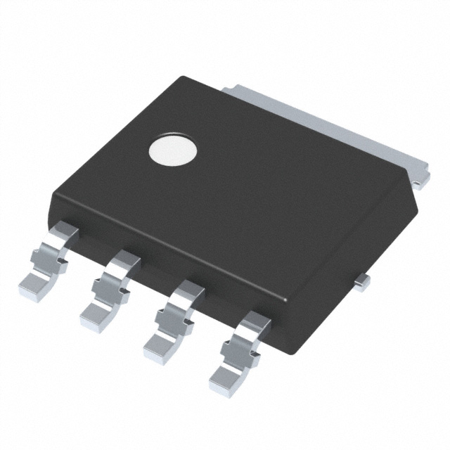
HP620L
ALLYW
LFPAK4
CASE 760AB
Mechanical Characteristics:
•
•
•
•
5
1,2,3,4
1
Device
Package
Shipping†
NHP620LFST1G
LFPAK4
(Pb−Free)
3000 /
Tape & Reel
NRVHP620LFST1G
LFPAK4
(Pb−Free)
3000 /
Tape & Reel
†For information on tape and reel specifications,
including part orientation and tape sizes, please
refer to our Tape and Reel Packaging Specification
Brochure, BRD8011/D.
Publication Order Number:
NHP620LFS/D
�NHP620LFS, NRVHP620LFS
MAXIMUM RATINGS
Rating
Symbol
Value
Unit
Peak Repetitive Reverse Voltage
Working Peak Reverse Voltage
DC Blocking Voltage
VRRM
VRWM
VR
V
200
Average Rectified Forward Current
(Rated VR, TC = 169°C)
IF(AV)
6.0
A
Peak Repetitive Forward Current,
(Rated VR, Square Wave, 20 kHz, TC = 160°C)
IFRM
12
A
Non−Repetitive Peak Surge Current
(Surge Applied at Rated Load Conditions Halfwave, Single Phase, 60 Hz)
IFSM
150
A
Storage Temperature Range
Tstg
−65 to +175
°C
Operating Junction Temperature
TJ
−55 to +175
°C
ESD Rating (Human Body Model)
3B
ESD Rating (Machine Model)
C
Stresses exceeding those listed in the Maximum Ratings table may damage the device. If any of these limits are exceeded, device functionality
should not be assumed, damage may occur and reliability may be affected.
THERMAL CHARACTERISTICS
Symbol
Max
Unit
Thermal Resistance, Junction−to−Case, Steady State
(Assumes 600 mm2 1 oz. copper bond pad, on a FR4 board)
Characteristic
RθJC
1.31
°C/W
Thermal Resistance, Junction−to−Ambient, Steady State
(Assumes 600 mm2 1 oz. copper bond pad, on a FR4 board)
RθJA
44.4
°C/W
Symbol
Max
Unit
ELECTRICAL CHARACTERISTICS
Characteristic
Instantaneous Forward Voltage (Note 1)
(iF = 6 A, TJ = 125°C)
(iF = 6 A, TJ = 25°C)
(iF = 3 A, TJ = 125°C)
(iF = 3 A, TJ = 25°C)
vF
Instantaneous Reverse Current (Note 1)
(Rated dc Voltage, TJ = 125°C)
(Rated dc Voltage, TJ = 25°C)
iR
Maximum Reverse Recovery Time
(IF = 1.0 A, di/dt = 50 A/ms, VR = 30 V)
Trr
0.80
0.95
0.73
0.87
75
0.5
50
V
mA
ns
Product parametric performance is indicated in the Electrical Characteristics for the listed test conditions, unless otherwise noted. Product
performance may not be indicated by the Electrical Characteristics if operated under different conditions.
1. Pulse Test: Pulse Width = 300 ms, Duty Cycle ≤ 2.0%.
www.onsemi.com
2
�NHP620LFS, NRVHP620LFS
TYPICAL CHARACTERISTICS
10
iF, INSTANTANEOUS FORWARD
CURRENT (A)
100
TA = 175°C
TA = 150°C
TA = 125°C
1
TA = 85°C
TA = 25°C
TA = −55°C
0
IR, INSTANTANEOUS REVERSE CURRENT (A)
0.1
0.2
0.4
0.6
0.8
1.0
1.2
TA = 150°C
TA = 125°C
1
0.1
1.4
TA = 175°C
TA = 25°C
TA = −55°C
0.6
0.8
1.0
1.2
1.4
Figure 2. Maximum Instantaneous Forward
Characteristics
1.6
1.E−02
1.E−03
TA = 175°C
TA = 150°C
TA = 150°C
1.E−05
TA = 85°C
1.E−07
TA = 175°C
1.E−04
TA = 125°C
1.E−06
TA = 125°C
1.E−06
1.E−08
TA = 25°C
1.E−09
TA = −55°C
1.E−10
20
40
60
80
100
120
140
160 180 200
TA = 85°C
1.E−07
TA = 25°C
1.E−08
TA = −55°C
1.E−09
20
40
60
80
100
120 140
160 180 200
VR, INSTANTANEOUS REVERSE VOLTAGE (V)
VR, INSTANTANEOUS REVERSE VOLTAGE (V)
Figure 3. Typical Reverse Characteristics
Figure 4. Maximum Reverse Characteristics
1000
C, JUNCTION CAPACITANCE (pF)
0.4
Figure 1. Typical Instantaneous Forward
Characteristics
1.E−05
TJ = 25°C
100
0.1
0.2
0
VF, INSTANTANEOUS FORWARD VOLTAGE (V)
1.E−04
10
TA = 85°C
VF, INSTANTANEOUS FORWARD VOLTAGE (V)
1.E−03
1.E−11
10
IR, INSTANTANEOUS REVERSE CURRENT (A)
iF, INSTANTANEOUS FORWARD
CURRENT (A)
100
1
10
100
VR, REVERSE VOLTAGE (V)
Figure 5. Typical Junction Capacitance
www.onsemi.com
3
�NHP620LFS, NRVHP620LFS
TYPICAL CHARACTERISTICS
6
100
IF(AV), AVERAGE FORWARD
CURRENT (A)
80
DC
70
60
50
Square Wave
(Duty = 0.5)
40
30
20
10
0
25
40
55
70
85
TJ = 175°C
PF(AV), AVERAGE FORWARD
POWER DISSIPATION (W)
RqJC = 1.31°C/W
TJ = 175°C
90
5
4
3
DC
2
1
0
100 115 130 145 160 175
Square Wave
(Duty = 0.5)
0
1
2
3
4
5
TC, CASE TEMPERATURE (°C)
IF(AV), AVERAGE FORWARD CURRENT (A)
Figure 6. Current Derating per Device
Figure 7. Forward Power Dissipation
6
100
50% Duty Cycle
R(t) (°C/W)
10
1
20%
10%
5%
2%
1%
0.1
0.01
Single Pulse
0.001
0.0000001 0.000001 0.00001
0.0001
0.001
0.01
0.1
1
PULSE TIME (sec)
Figure 8. Typical Thermal Characteristics, Junction−to−Ambient
www.onsemi.com
4
10
100
1000
�MECHANICAL CASE OUTLINE
PACKAGE DIMENSIONS
LFPAK4 5x6
CASE 760AB
ISSUE C
GENERIC
MARKING DIAGRAM*
XXXXXX
XXXXXX
AWLYW
DOCUMENT NUMBER:
DESCRIPTION:
98AON82777G
LFPAK4 5x6
XXXXXX
A
WL
Y
W
DATE 19 NOV 2019
= Specific Device Code
= Assembly Location
= Wafer Lot
= Year
= Work Week
*This information is generic. Please refer
to device data sheet for actual part
marking. Some products may not follow
the Generic Marking.
Electronic versions are uncontrolled except when accessed directly from the Document Repository.
Printed versions are uncontrolled except when stamped “CONTROLLED COPY” in red.
PAGE 1 OF 1
ON Semiconductor and
are trademarks of Semiconductor Components Industries, LLC dba ON Semiconductor or its subsidiaries in the United States and/or other countries.
ON Semiconductor reserves the right to make changes without further notice to any products herein. ON Semiconductor makes no warranty, representation or guarantee regarding
the suitability of its products for any particular purpose, nor does ON Semiconductor assume any liability arising out of the application or use of any product or circuit, and specifically
disclaims any and all liability, including without limitation special, consequential or incidental damages. ON Semiconductor does not convey any license under its patent rights nor the
rights of others.
© Semiconductor Components Industries, LLC, 2018
www.onsemi.com
�onsemi,
, and other names, marks, and brands are registered and/or common law trademarks of Semiconductor Components Industries, LLC dba “onsemi” or its affiliates
and/or subsidiaries in the United States and/or other countries. onsemi owns the rights to a number of patents, trademarks, copyrights, trade secrets, and other intellectual property.
A listing of onsemi’s product/patent coverage may be accessed at www.onsemi.com/site/pdf/Patent−Marking.pdf. onsemi reserves the right to make changes at any time to any
products or information herein, without notice. The information herein is provided “as−is” and onsemi makes no warranty, representation or guarantee regarding the accuracy of the
information, product features, availability, functionality, or suitability of its products for any particular purpose, nor does onsemi assume any liability arising out of the application or use
of any product or circuit, and specifically disclaims any and all liability, including without limitation special, consequential or incidental damages. Buyer is responsible for its products
and applications using onsemi products, including compliance with all laws, regulations and safety requirements or standards, regardless of any support or applications information
provided by onsemi. “Typical” parameters which may be provided in onsemi data sheets and/or specifications can and do vary in different applications and actual performance may
vary over time. All operating parameters, including “Typicals” must be validated for each customer application by customer’s technical experts. onsemi does not convey any license
under any of its intellectual property rights nor the rights of others. onsemi products are not designed, intended, or authorized for use as a critical component in life support systems
or any FDA Class 3 medical devices or medical devices with a same or similar classification in a foreign jurisdiction or any devices intended for implantation in the human body. Should
Buyer purchase or use onsemi products for any such unintended or unauthorized application, Buyer shall indemnify and hold onsemi and its officers, employees, subsidiaries, affiliates,
and distributors harmless against all claims, costs, damages, and expenses, and reasonable attorney fees arising out of, directly or indirectly, any claim of personal injury or death
associated with such unintended or unauthorized use, even if such claim alleges that onsemi was negligent regarding the design or manufacture of the part. onsemi is an Equal
Opportunity/Affirmative Action Employer. This literature is subject to all applicable copyright laws and is not for resale in any manner.
PUBLICATION ORDERING INFORMATION
LITERATURE FULFILLMENT:
Email Requests to: orderlit@onsemi.com
onsemi Website: www.onsemi.com
◊
TECHNICAL SUPPORT
North American Technical Support:
Voice Mail: 1 800−282−9855 Toll Free USA/Canada
Phone: 011 421 33 790 2910
Europe, Middle East and Africa Technical Support:
Phone: 00421 33 790 2910
For additional information, please contact your local Sales Representative
�


 工商网监
湘ICP备2023018690号
工商网监
湘ICP备2023018690号
