NTB6412AN, NTP6412AN,
NVB6412AN
N-Channel Power MOSFET
100 V, 58 A, 18.2 mW
Features
•
•
•
•
•
Low RDS(on)
High Current Capability
100% Avalanche Tested
NVB Prefix for Automotive and Other Applications Requiring
Unique Site and Control Change Requirements; AEC−Q101
Qualified and PPAP Capable
These Devices are Pb−Free and are RoHS Compliant
www.onsemi.com
V(BR)DSS
100 V
N−Channel
D
Symbol
Value
Unit
Drain−to−Source Voltage
VDSS
100
V
Gate−to−Source Voltage − Continuous
VGS
$20
V
ID
58
A
Continuous Drain Current RqJC
Steady
State
Power Dissipation
RqJC
Steady
State
TC = 25°C
TC = 100°C
S
167
W
IDM
240
A
TJ, Tstg
−55 to
+175
°C
IS
58
A
Single Pulse Drain−to−Source Avalanche
Energy (VDD = 50 Vdc, VGS = 10 Vdc,
IL(pk) = 44.7 A, L = 0.3 mH, RG = 25 W)
EAS
300
mJ
Lead Temperature for Soldering
Purposes, 1/8″ from Case for 10 Seconds
TL
tp = 10 ms
Operating Junction and Storage Temperature
Range
Source Current (Body Diode)
G
41
PD
Pulsed Drain Current
TC = 25°C
4
4
1
2
3
1
2
3
4
Drain
Symbol
Max
Unit
Junction−to−Case (Drain) Steady State
RqJC
0.9
°C/W
Junction−to−Ambient (Note 1)
RqJA
33
Stresses exceeding those listed in the Maximum Ratings table may damage the
device. If any of these limits are exceeded, device functionality should not be
assumed, damage may occur and reliability may be affected.
1. Surface mounted on FR4 board using 1 sq in pad size,
(Cu Area 1.127 sq in [2 oz] including traces).
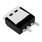
D2PAK
CASE 418B
STYLE 2
TO−220AB
CASE 221A
STYLE 5
°C
260
THERMAL RESISTANCE RATINGS
Parameter
58 A
18.2 mW @ 10 V
MAXIMUM RATINGS (TJ = 25°C Unless otherwise specified)
Parameter
ID MAX
(Note 1)
RDS(ON) MAX
MARKING DIAGRAM
& PIN ASSIGNMENT
4
Drain
NTB
6412ANG
AYWW
NTP
6412ANG
AYWW
1
Gate
3
Source
2
Drain
1
Gate
2
Drain
3
Source
6412AN = Specific Device Code
G
= Pb−Free Device
A
= Assembly Location
Y
= Year
WW = Work Week
ORDERING INFORMATION
See detailed ordering and shipping information in the package
dimensions section on page 5 of this data sheet.
© Semiconductor Components Industries, LLC, 2015
January, 2015 − Rev. 2
1
Publication Order Number:
NTB6412AN/D
�NTB6412AN, NTP6412AN, NVB6412AN
ELECTRICAL CHARACTERISTICS (TJ = 25°C Unless otherwise specified)
Characteristics
Symbol
Test Condition
Min
V(BR)DSS
VGS = 0 V, ID = 250 mA
100
Typ
Max
Unit
OFF CHARACTERISTICS
Drain−to−Source Breakdown Voltage
Drain−to−Source Breakdown Voltage Temperature Coefficient
Zero Gate Voltage Drain Current
Gate−to−Source Leakage Current
V(BR)DSS/TJ
IDSS
V
103
VGS = 0 V,
VDS = 100 V
mV/°C
TJ = 25°C
1.0
TJ = 125°C
100
IGSS
VDS = 0 V, VGS = $20 V
VGS(th)
VGS = VDS, ID = 250 mA
$100
mA
nA
ON CHARACTERISTICS (Note 2)
Gate Threshold Voltage
Negative Threshold Temperature Coefficient
Drain−to−Source On−Resistance
VGS(th)/TJ
4.0
9.2
RDS(on)
Forward Transconductance
2.0
gFS
V
mV/°C
VGS = 10 V, ID = 58 A
16.8
18.2
VGS = 10 V, ID = 20 A
15.6
18.2
VDS = 5 V, ID = 20 A
31
mW
S
CHARGES, CAPACITANCES & GATE RESISTANCE
Input Capacitance
Ciss
Output Capacitance
Coss
Reverse Transfer Capacitance
Crss
150
Total Gate Charge
QG(TOT)
73
Threshold Gate Charge
QG(TH)
VDS = 25 V, VGS = 0 V,
f = 1 MHz
2700
3500
400
500
100
pF
nC
2.5
VGS = 10 V, VDS = 80 V,
ID = 58 A
Gate−to−Source Charge
QGS
13.5
Gate−to−Drain Charge
QGD
35
Plateau Voltage
VGP
5.6
V
Gate Resistance
RG
2.2
W
16
ns
SWITCHING CHARACTERISTICS, VGS = 10 V (Note 3)
Turn−On Delay Time
Rise Time
Turn−Off Delay Time
Fall Time
td(on)
tr
td(off)
VGS = 10 V, VDD = 80 V,
ID = 58 A, RG = 6.2 W
tf
140
70
126
DRAIN−SOURCE DIODE CHARACTERISTICS
Forward Diode Voltage
VSD
Reverse Recovery Time
trr
Charge Time
ta
Discharge Time
Reverse Recovery Charge
IS = 58 A
TJ = 25°C
0.96
TJ = 125°C
0.89
85
VGS = 0 V, IS = 58 A,
dISD/dt = 100 A/ms
tb
QRR
www.onsemi.com
2
V
ns
60
25
270
2. Pulse Test: Pulse Width ≤ 300 ms, Duty Cycle ≤ 2%.
3. Switching characteristics are independent of operating junction temperatures.
1.3
nC
�NTB6412AN, NTP6412AN, NVB6412AN
120
120
7.5 V
100
6.5 V
ID, DRAIN CURRENT (A)
ID, DRAIN CURRENT (A)
TJ = 25°C
10 V
80
6.0 V
60
5.4 V
40
5.0 V
20
VDS w 10 V
100
80
60
40
20
VGS = 4.4 V
TJ = −55°C
0
1
2
3
4
5
2
4
5
6
7
VDS, DRAIN−TO−SOURCE VOLTAGE (V)
Figure 1. On−Region Characteristics
Figure 2. Transfer Characteristics
0.04
ID = 58 A
TJ = 25°C
0.03
0.02
0.01
5
6
7
8
9
10
VGS, GATE−TO−SOURCE VOLTAGE (V)
8
0.06
VGS = 10 V
0.05
TJ = 175°C
0.04
TJ = 125°C
0.03
0.02
TJ = 25°C
TJ = −55°C
0.01
0
10
20
30
40
50
60
ID, DRAIN CURRENT (A)
Figure 3. On−Region versus Gate Voltage
Figure 4. On−Resistance versus Drain Current
and Gate Voltage
3
100000
VGS = 0 V
ID = 58 A
VGS = 10 V
IDSS, LEAKAGE (nA)
RDS(on), DRAIN−TO−SOURCE RESISTANCE
(NORMALIZED)
3
VGS, GATE−TO−SOURCE VOLTAGE (V)
RDS(on), DRAIN−TO−SOURCE RESISTANCE (W)
RDS(on), DRAIN−TO−SOURCE RESISTANCE (W)
0
0
2.5
TJ = 25°C
TJ = 125°C
2
1.5
10000
TJ = 150°C
TJ = 125°C
1000
1
0.5
−50
100
−25
0
25
50
75
100
125
150
175
10
20
30
40
50
60
70
80
90 100
TJ, JUNCTION TEMPERATURE (°C)
VDS, DRAIN−TO−SOURCE VOLTAGE (V)
Figure 5. On−Resistance Variation with
Temperature
Figure 6. Drain−to−Source Leakage Current
versus Voltage
www.onsemi.com
3
�10
VGS, GATE−TO−SOURCE VOLTAGE (V)
5000
C, CAPACITANCE (pF)
TJ = 25°C
VGS = 0 V
4000
3000
Ciss
2000
1000
0
Coss
Crss
0
10 20 30 40 50 60 70 80 90
VDS, DRAIN−TO−SOURCE VOLTAGE (V)
8
VGS
VDS
80
Qgd
Qgs
6
60
4
40
2
VDS = 80 V
ID = 58 A
TJ = 25°C
0
100
Figure 7. Capacitance Variation
0
10
20
30
40
50
60
Qg, TOTAL GATE CHARGE (nC)
20
0
70
Figure 8. Gate−to−Source Voltage and
Drain−to−Source Voltage versus Total Charge
1000
100
IS, SOURCE CURRENT (A)
60
VDS = 80 V
ID = 58 A
VGS = 10 V
t, TIME (ns)
100
QT
VDS, DRAIN−TO−SOURCE VOLTAGE (V)
NTB6412AN, NTP6412AN, NVB6412AN
tf
tr
td(off)
td(on)
10
1
TJ = 25°C
VGS = 0 V
50
40
30
20
10
0
1
10
RG, GATE RESISTANCE (W)
0.5
100
Figure 9. Resistive Switching Time Variation
versus Gate Resistance
0.6
0.7
0.8
0.9
VSD, SOURCE−TO−DRAIN VOLTAGE (V)
1.0
Figure 10. Diode Forward Voltage versus
Current
1000
300
100
AVALANCHE ENERGY (mJ)
ID, DRAIN CURRENT (A)
ID = 44.7 A
10 ms
100 ms
10
1 ms
10 ms
dc
1
RDS(on) LIMIT
THERMAL LIMIT
PACKAGE LIMIT
VGS = 10 V
SINGLE PULSE
TC = 25°C
10
100
VDS, DRAIN−TO−SOURCE VOLTAGE (V)
100
0
0.1
1
200
1000
25
Figure 11. Maximum Rated Forward Biased
Safe Operating Area
50
75
100
125
150
TJ, STARTING JUNCTION TEMPERATURE
175
Figure 12. Maximum Avalanche Energy versus
Starting Junction Temperature
www.onsemi.com
4
�NTB6412AN, NTP6412AN, NVB6412AN
1
D = 0.5
0.2
R(t) (°C/W)
0.1
0.1
0.05
0.02
0.01
0.01
0.001
0.000001
SINGLE PULSE
0.00001
0.0001
0.001
0.01
0.1
t, PULSE TIME (s)
1
10
100
1000
Figure 13. Thermal Response
ORDERING INFORMATION
Package
Shipping†
NTB6412ANG
D2PAK
(Pb−Free)
50 Units / Rail
NTB6412ANT4G
D2PAK
(Pb−Free)
800 / Tape & Reel
NTP6412ANG
TO−220
(Pb−Free)
50 Units / Rail
NVB6412ANT4G
D2PAK
(Pb−Free)
800 / Tape & Reel
Device
†For information on tape and reel specifications, including part orientation and tape sizes, please refer to our Tape and Reel Packaging
Specifications Brochure, BRD8011/D.
www.onsemi.com
5
�MECHANICAL CASE OUTLINE
PACKAGE DIMENSIONS
TO−220
CASE 221A
ISSUE AK
DATE 13 JAN 2022
SCALE 1:1
STYLE 1:
PIN 1.
2.
3.
4.
BASE
COLLECTOR
EMITTER
COLLECTOR
STYLE 2:
PIN 1.
2.
3.
4.
BASE
EMITTER
COLLECTOR
EMITTER
STYLE 3:
PIN 1.
2.
3.
4.
CATHODE
ANODE
GATE
ANODE
STYLE 4:
PIN 1.
2.
3.
4.
MAIN TERMINAL 1
MAIN TERMINAL 2
GATE
MAIN TERMINAL 2
STYLE 5:
PIN 1.
2.
3.
4.
GATE
DRAIN
SOURCE
DRAIN
STYLE 6:
PIN 1.
2.
3.
4.
ANODE
CATHODE
ANODE
CATHODE
STYLE 7:
PIN 1.
2.
3.
4.
CATHODE
ANODE
CATHODE
ANODE
STYLE 8:
PIN 1.
2.
3.
4.
CATHODE
ANODE
EXTERNAL TRIP/DELAY
ANODE
STYLE 9:
PIN 1.
2.
3.
4.
GATE
COLLECTOR
EMITTER
COLLECTOR
STYLE 10:
PIN 1.
2.
3.
4.
GATE
SOURCE
DRAIN
SOURCE
STYLE 11:
PIN 1.
2.
3.
4.
DRAIN
SOURCE
GATE
SOURCE
STYLE 12:
PIN 1.
2.
3.
4.
MAIN TERMINAL 1
MAIN TERMINAL 2
GATE
NOT CONNECTED
DOCUMENT NUMBER:
DESCRIPTION:
98ASB42148B
TO−220
Electronic versions are uncontrolled except when accessed directly from the Document Repository.
Printed versions are uncontrolled except when stamped “CONTROLLED COPY” in red.
PAGE 1 OF 1
onsemi and
are trademarks of Semiconductor Components Industries, LLC dba onsemi or its subsidiaries in the United States and/or other countries. onsemi reserves
the right to make changes without further notice to any products herein. onsemi makes no warranty, representation or guarantee regarding the suitability of its products for any particular
purpose, nor does onsemi assume any liability arising out of the application or use of any product or circuit, and specifically disclaims any and all liability, including without limitation
special, consequential or incidental damages. onsemi does not convey any license under its patent rights nor the rights of others.
© Semiconductor Components Industries, LLC, 2019
www.onsemi.com
�MECHANICAL CASE OUTLINE
PACKAGE DIMENSIONS
D2PAK 3
CASE 418B−04
ISSUE L
DATE 17 FEB 2015
SCALE 1:1
NOTES:
1. DIMENSIONING AND TOLERANCING
PER ANSI Y14.5M, 1982.
2. CONTROLLING DIMENSION: INCH.
3. 418B−01 THRU 418B−03 OBSOLETE,
NEW STANDARD 418B−04.
C
E
−B−
V
W
4
1
2
A
S
3
−T−
SEATING
PLANE
K
W
J
G
D
DIM
A
B
C
D
E
F
G
H
J
K
L
M
N
P
R
S
V
H
3 PL
0.13 (0.005)
M
T B
M
VARIABLE
CONFIGURATION
ZONE
N
R
P
L
M
STYLE 1:
PIN 1. BASE
2. COLLECTOR
3. EMITTER
4. COLLECTOR
L
M
F
F
F
VIEW W−W
1
VIEW W−W
2
VIEW W−W
3
STYLE 2:
PIN 1. GATE
2. DRAIN
3. SOURCE
4. DRAIN
MILLIMETERS
MIN
MAX
8.64
9.65
9.65 10.29
4.06
4.83
0.51
0.89
1.14
1.40
7.87
8.89
2.54 BSC
2.03
2.79
0.46
0.64
2.29
2.79
1.32
1.83
7.11
8.13
5.00 REF
2.00 REF
0.99 REF
14.60 15.88
1.14
1.40
U
L
M
INCHES
MIN
MAX
0.340 0.380
0.380 0.405
0.160 0.190
0.020 0.035
0.045 0.055
0.310 0.350
0.100 BSC
0.080
0.110
0.018 0.025
0.090
0.110
0.052 0.072
0.280 0.320
0.197 REF
0.079 REF
0.039 REF
0.575 0.625
0.045 0.055
STYLE 3:
PIN 1. ANODE
2. CATHODE
3. ANODE
4. CATHODE
STYLE 4:
PIN 1. GATE
2. COLLECTOR
3. EMITTER
4. COLLECTOR
STYLE 5:
STYLE 6:
PIN 1. CATHODE
PIN 1. NO CONNECT
2. ANODE
2. CATHODE
3. CATHODE
3. ANODE
4. ANODE
4. CATHODE
MARKING INFORMATION AND FOOTPRINT ON PAGE 2
DOCUMENT NUMBER:
DESCRIPTION:
98ASB42761B
D2PAK 3
Electronic versions are uncontrolled except when accessed directly from the Document Repository.
Printed versions are uncontrolled except when stamped “CONTROLLED COPY” in red.
PAGE 1 OF 2
ON Semiconductor and
are trademarks of Semiconductor Components Industries, LLC dba ON Semiconductor or its subsidiaries in the United States and/or other countries.
ON Semiconductor reserves the right to make changes without further notice to any products herein. ON Semiconductor makes no warranty, representation or guarantee regarding
the suitability of its products for any particular purpose, nor does ON Semiconductor assume any liability arising out of the application or use of any product or circuit, and specifically
disclaims any and all liability, including without limitation special, consequential or incidental damages. ON Semiconductor does not convey any license under its patent rights nor the
rights of others.
© Semiconductor Components Industries, LLC, 2019
www.onsemi.com
�D2PAK 3
CASE 418B−04
ISSUE L
DATE 17 FEB 2015
GENERIC
MARKING DIAGRAM*
xx
xxxxxxxxx
AWLYWWG
xxxxxxxxG
AYWW
AYWW
xxxxxxxxG
AKA
IC
Standard
Rectifier
xx
A
WL
Y
WW
G
AKA
= Specific Device Code
= Assembly Location
= Wafer Lot
= Year
= Work Week
= Pb−Free Package
= Polarity Indicator
*This information is generic. Please refer to
device data sheet for actual part marking.
Pb−Free indicator, “G” or microdot “ G”,
may or may not be present.
SOLDERING FOOTPRINT*
10.49
8.38
16.155
2X
3.504
2X
1.016
5.080
PITCH
DIMENSIONS: MILLIMETERS
*For additional information on our Pb−Free strategy and soldering
details, please download the ON Semiconductor Soldering and
Mounting Techniques Reference Manual, SOLDERRM/D.
DOCUMENT NUMBER:
DESCRIPTION:
98ASB42761B
D2PAK 3
Electronic versions are uncontrolled except when accessed directly from the Document Repository.
Printed versions are uncontrolled except when stamped “CONTROLLED COPY” in red.
PAGE 2 OF 2
ON Semiconductor and
are trademarks of Semiconductor Components Industries, LLC dba ON Semiconductor or its subsidiaries in the United States and/or other countries.
ON Semiconductor reserves the right to make changes without further notice to any products herein. ON Semiconductor makes no warranty, representation or guarantee regarding
the suitability of its products for any particular purpose, nor does ON Semiconductor assume any liability arising out of the application or use of any product or circuit, and specifically
disclaims any and all liability, including without limitation special, consequential or incidental damages. ON Semiconductor does not convey any license under its patent rights nor the
rights of others.
© Semiconductor Components Industries, LLC, 2019
www.onsemi.com
�onsemi,
, and other names, marks, and brands are registered and/or common law trademarks of Semiconductor Components Industries, LLC dba “onsemi” or its affiliates
and/or subsidiaries in the United States and/or other countries. onsemi owns the rights to a number of patents, trademarks, copyrights, trade secrets, and other intellectual property.
A listing of onsemi’s product/patent coverage may be accessed at www.onsemi.com/site/pdf/Patent−Marking.pdf. onsemi reserves the right to make changes at any time to any
products or information herein, without notice. The information herein is provided “as−is” and onsemi makes no warranty, representation or guarantee regarding the accuracy of the
information, product features, availability, functionality, or suitability of its products for any particular purpose, nor does onsemi assume any liability arising out of the application or use
of any product or circuit, and specifically disclaims any and all liability, including without limitation special, consequential or incidental damages. Buyer is responsible for its products
and applications using onsemi products, including compliance with all laws, regulations and safety requirements or standards, regardless of any support or applications information
provided by onsemi. “Typical” parameters which may be provided in onsemi data sheets and/or specifications can and do vary in different applications and actual performance may
vary over time. All operating parameters, including “Typicals” must be validated for each customer application by customer’s technical experts. onsemi does not convey any license
under any of its intellectual property rights nor the rights of others. onsemi products are not designed, intended, or authorized for use as a critical component in life support systems
or any FDA Class 3 medical devices or medical devices with a same or similar classification in a foreign jurisdiction or any devices intended for implantation in the human body. Should
Buyer purchase or use onsemi products for any such unintended or unauthorized application, Buyer shall indemnify and hold onsemi and its officers, employees, subsidiaries, affiliates,
and distributors harmless against all claims, costs, damages, and expenses, and reasonable attorney fees arising out of, directly or indirectly, any claim of personal injury or death
associated with such unintended or unauthorized use, even if such claim alleges that onsemi was negligent regarding the design or manufacture of the part. onsemi is an Equal
Opportunity/Affirmative Action Employer. This literature is subject to all applicable copyright laws and is not for resale in any manner.
PUBLICATION ORDERING INFORMATION
LITERATURE FULFILLMENT:
Email Requests to: orderlit@onsemi.com
onsemi Website: www.onsemi.com
◊
TECHNICAL SUPPORT
North American Technical Support:
Voice Mail: 1 800−282−9855 Toll Free USA/Canada
Phone: 011 421 33 790 2910
Europe, Middle East and Africa Technical Support:
Phone: 00421 33 790 2910
For additional information, please contact your local Sales Representative
�


 工商网监
湘ICP备2023018690号
工商网监
湘ICP备2023018690号

