Ultrafast Power Rectifier
6 A, 600 V
RURD660S9A-F085
The RURD660S9A−F085 is an ultrafast diode with soft recovery
characteristics (trr < 83 ns). It has a low forward voltage drop and is of
silicon nitride passivated ion−implanted epitaxial planar construction.
This device is intended for use as a freewheeling/clamping diode and
rectifier in a variety of switching power supplies and other power
switching applications. Its low stored charge and ultrafast soft
recovery minimize ringing and electrical noise in many power
switching circuits, thus reducing powerloss in the switching
transistors.
www.onsemi.com
1, 2, 4. Cathode
3. Anode
Features
•
•
•
•
•
High Speed Switching (trr = 63 ns (Typ.) @ IF = 6 A)
Low Forward Voltage (VF = 1.26 V (Typ.) @ IF = 6 A)
Avalanche Energy Rated
AEC−Q101 Qualified and PPAP Capable
This is a Pb−Free Device
4
1
3
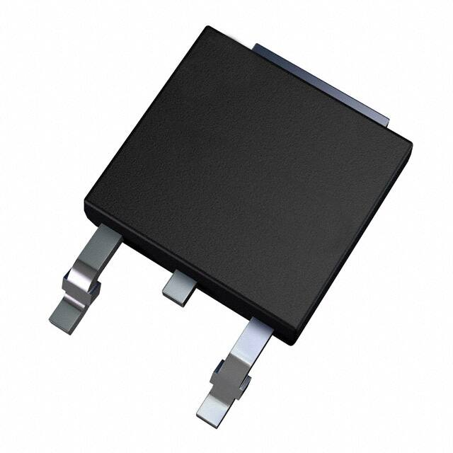
DPAK3 (TO−252 3 LD)
CASE 369AS
Applications
• General Purpose
• Switching Mode Power Supply
• Power Switching Circuits
MARKING DIAGRAM
$Y&Z&3&K
RUR660
ABSOLUTE MAXIMUM RATINGS (TC = 25°C unless otherwise noted)
Symbol
Parameter
Ratings
Unit
VRRM
Peak Repetitive Reverse Voltage
600
V
VRWM
Working Peak Reverse Voltage
600
V
DC Blocking Voltage
600
V
6
A
VR
IF(AV)
Average Rectified Forward Current
@ TC = 25°C
IFSM
Non−repetitive Peak Surge Current
TJ, TSTG
Operating Junction and Storage
Temperature
2
60
A
− 55 to +175
°C
RUR660
$Y
&Z
&3
&K
= Specific Device Code
= ON Semiconductor Logo
= Assembly Plant Code
= 3−Digit Date Code
= 2−Digits Lot Run Traceability Code
ORDERING INFORMATION
See detailed ordering and shipping information on page 4 of
this data sheet.
Stresses exceeding those listed in the Maximum Ratings table may damage the
device. If any of these limits are exceeded, device functionality should not be
assumed, damage may occur and reliability may be affected.
THERMAL CHARACTERISTICS (TC = 25°C unless otherwise noted)
Parameter
Symbol
Max
Unit
RqJC
Maximum Thermal Resistance,
Junction to Case
3
°C/W
RqJA
(Note 1)
Maximum Thermal Resistance,
Junction to Ambient
140
°C/W
RqJA
(Note 2)
Maximum Thermal Resistance,
Junction to Ambient
50
°C/W
1. Mounted on a minimum pad follow by JEDEC standard.
2. Mounted on a 1 in2 pad of 2 oz copper follow by JEDEC standard.
© Semiconductor Components Industries, LLC, 2013
July, 2020 − Rev. 4
1
Publication Order Number:
RURD660S9A−F085/D
�RURD660S9A−F085
ELECTRICAL CHARACTERISTICS (TC = 25°C unless otherwise noted)
Symbol
IR
Parameter
Condition
Instantaneous Reverse
Current
VR = 600 V
Min
Typ
Max
Unit
TC = 25°C
−
−
100
mA
TC = 175°
−
−
500
mA
VFM
Instantaneous Forward
(Note 3) Voltage
IF = 6 A
TC = 25°C
TC = 175°
−
−
1.26
1.04
1.5
−
V
V
trr
Reverse Recovery Time
(Note 4)
IF = 1 A, di/dt = 200 A/ms, VCC = 390 V
TC = 25°C
−
25
33
ns
IF = 6 A, di/dt = 200 A/ms, VCC = 390 V
TC = 25°C
TC = 175°
−
−
63
119
83
−
ns
ns
IF = 6 A, di/dt = 200 A/ms, VCC = 390 V
TC = 25°C
−
−
−
23
40
151
−
−
−
ns
ns
nC
10
−
−
mJ
ta
tb
Qrr
Reverse Recovery Time
Reverse Recovery Charge
WAVL
Avalanche Energy (L = 20 mH)
Product parametric performance is indicated in the Electrical Characteristics for the listed test conditions, unless otherwise noted. Product
performance may not be indicated by the Electrical Characteristics if operated under different conditions.
3. Pulse: Test Pulse width = 300 ms, Duty Cycle = 2%
4. Guaranteed by design
TEST CIRCUIT AND WAVEFORMS
VGE AMPLITUDE AND
RG CONTROL dIF/dt
t1 AND t2 CONTROL IF
L
DUT
CURRENT
SENSE
RG
VGE
dI F
t rr
dt
ta
0
VDD
−
IGBT
t1
IF
+
tb
0.25 IRM
t2
IRM
Figure 1. trr Test Circuit
I=1A
L = 20 Mh
R < 0.1 W
EAVL = 1/2LI2 [VR(AVL) / (VR(AVL) − VDD)]
Q1 = IGBT (BVCES > DUT VR(AVL))
Figure 2. trr Waveforms and Definitions
VAVL
L
R
CURRENT
SENSE
+
VDD
IL
IL
I V
Q1
VDD
DUT
−
t0
Figure 3. Avalanche Energy Test Circuit
t1
t2
t
Figure 4. Avalanche Current and Voltage Waveforms
www.onsemi.com
2
�RURD660S9A−F085
TYPICAL PERFORMANCE CHARACTERISTICS
100
100
IR, Forward Current (mA)
IF, Forward Current (A)
TC = 175°C
10
TC = 175°C
TC = 125°C
1
TC = 25°C
0.1
0.1
0.5
1.0
1.5
2.0
10
TC = 125°C
1
0.1
TC = 25°C
0.01
2.5
100
200
VF, Forward Voltage (V)
trr, Reverse Recovery Time (ns)
Cj, Capacitance (pF)
180
60
40
20
10
0.1
1
10
150
TC = 175°C
120
90
TC = 125°C
60
TC = 25°C
30
100
100
200
300
400
500
di/dt (A/ms)
Figure 5. Typical Junction Capacitance
Figure 6. Typical Reverse Recovery Time vs. di/dt
15
35
IF(AV), Average Forward Current (A)
trr, Reverse Recovery Current (A)
600
IF = 6 A
VR, Reverse Voltage (V)
TC = 175°C
10
TC = 125°C
5
0
100
500
Figure 10. Typical Reverse Current
vs. Reverse Voltage
Typical Capacitance
at 10 V = 24 pF
80
400
VR, Reverse Voltage (V)
Figure 9. Typical Forward Voltage Drop vs.
Forward Current
90
300
TC = 25°C
IF = 6 A
200
300
400
30
20
10
0
500
25
50
75
100
125
150
TC, Case Temperature (°C)
di/dt (A/ms)
Figure 7. Typical Reverse Recovery Current vs. di/dt
Figure 8. Forward Current Derating Curve
www.onsemi.com
3
175
�RURD660S9A−F085
TYPICAL PERFORMANCE CHARACTERISTICS (continued)
Qrr, Reverse Recovery Charge (nC)
800
IF = 6 A
TC = 175°C
600
TC = 125°C
400
TC = 25°C
200
0
100
200
300
400
500
di/dt [A/ms]
Figure 12. Reverse Recovery Charge
ZthJC, Thermal Response (t)
10
1
D = 0.5
0.2
0.1
0.05
0.02
0.01
PDM
t1
t2
0.1
single pulse
0.01
10−5
10−4
*NOTES:
1. RthJC = 1.7°C/W Typ.
2. Duty Factor, D = t1 / t2
3. TJM − TC = PDM x ZthJC (t)
10−3
10−2
10−1
100
101
102
t1, Square Wave Pulse Duration (sec)
Figure 11. Transient Thermal Response Curve
ORDERING INFORMATION
Device
Device Marking
Package
Shipping†
RURD660S9A−F085
RUR660
TO−252 3 LD
(Pb−Free)
2500 / Tape & Reel
†For information on tape and reel specifications, including part orientation and tape sizes, please refer to our Tape and Reel Packaging
Specifications Brochure, BRD8011/D.
www.onsemi.com
4
�MECHANICAL CASE OUTLINE
PACKAGE DIMENSIONS
DPAK3 (TO−252 3 LD)
CASE 369AS
ISSUE O
DOCUMENT NUMBER:
DESCRIPTION:
98AON13810G
DPAK3 (TO−252 3 LD)
DATE 30 SEP 2016
Electronic versions are uncontrolled except when accessed directly from the Document Repository.
Printed versions are uncontrolled except when stamped “CONTROLLED COPY” in red.
PAGE 1 OF 1
ON Semiconductor and
are trademarks of Semiconductor Components Industries, LLC dba ON Semiconductor or its subsidiaries in the United States and/or other countries.
ON Semiconductor reserves the right to make changes without further notice to any products herein. ON Semiconductor makes no warranty, representation or guarantee regarding
the suitability of its products for any particular purpose, nor does ON Semiconductor assume any liability arising out of the application or use of any product or circuit, and specifically
disclaims any and all liability, including without limitation special, consequential or incidental damages. ON Semiconductor does not convey any license under its patent rights nor the
rights of others.
© Semiconductor Components Industries, LLC, 2019
www.onsemi.com
�onsemi,
, and other names, marks, and brands are registered and/or common law trademarks of Semiconductor Components Industries, LLC dba “onsemi” or its affiliates
and/or subsidiaries in the United States and/or other countries. onsemi owns the rights to a number of patents, trademarks, copyrights, trade secrets, and other intellectual property.
A listing of onsemi’s product/patent coverage may be accessed at www.onsemi.com/site/pdf/Patent−Marking.pdf. onsemi reserves the right to make changes at any time to any
products or information herein, without notice. The information herein is provided “as−is” and onsemi makes no warranty, representation or guarantee regarding the accuracy of the
information, product features, availability, functionality, or suitability of its products for any particular purpose, nor does onsemi assume any liability arising out of the application or use
of any product or circuit, and specifically disclaims any and all liability, including without limitation special, consequential or incidental damages. Buyer is responsible for its products
and applications using onsemi products, including compliance with all laws, regulations and safety requirements or standards, regardless of any support or applications information
provided by onsemi. “Typical” parameters which may be provided in onsemi data sheets and/or specifications can and do vary in different applications and actual performance may
vary over time. All operating parameters, including “Typicals” must be validated for each customer application by customer’s technical experts. onsemi does not convey any license
under any of its intellectual property rights nor the rights of others. onsemi products are not designed, intended, or authorized for use as a critical component in life support systems
or any FDA Class 3 medical devices or medical devices with a same or similar classification in a foreign jurisdiction or any devices intended for implantation in the human body. Should
Buyer purchase or use onsemi products for any such unintended or unauthorized application, Buyer shall indemnify and hold onsemi and its officers, employees, subsidiaries, affiliates,
and distributors harmless against all claims, costs, damages, and expenses, and reasonable attorney fees arising out of, directly or indirectly, any claim of personal injury or death
associated with such unintended or unauthorized use, even if such claim alleges that onsemi was negligent regarding the design or manufacture of the part. onsemi is an Equal
Opportunity/Affirmative Action Employer. This literature is subject to all applicable copyright laws and is not for resale in any manner.
PUBLICATION ORDERING INFORMATION
LITERATURE FULFILLMENT:
Email Requests to: orderlit@onsemi.com
onsemi Website: www.onsemi.com
◊
TECHNICAL SUPPORT
North American Technical Support:
Voice Mail: 1 800−282−9855 Toll Free USA/Canada
Phone: 011 421 33 790 2910
Europe, Middle East and Africa Technical Support:
Phone: 00421 33 790 2910
For additional information, please contact your local Sales Representative
�


 工商网监
湘ICP备2023018690号
工商网监
湘ICP备2023018690号
