SM05T1G�Series
ESD Protection Diode Array
Dual Common Anode
These dual monolithic silicon surge protection diodes are designed
for applications requiring transient overvoltage protection capability.
They are intended for use in voltage and ESD sensitive equipment such
as computers, printers, business machines, communication systems,
medical equipment and other applications. Their dual junction common
anode design protects two separate lines using only one package. These
devices are ideal for situations where board space is at a premium.
www.onsemi.com
Specification Features:
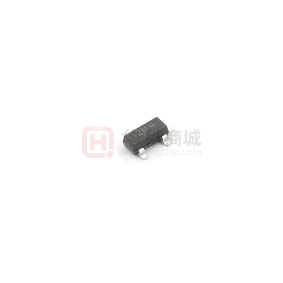
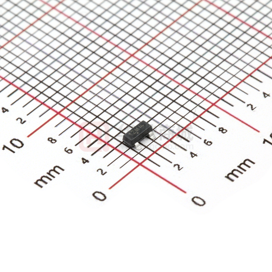
SOT−23
CASE 318
STYLE 12
• SOT−23 Package Allows Either Two Separate Unidirectional
•
•
•
•
•
•
Configurations or a Single Bidirectional Configuration
Working Peak Reverse Voltage Range − 5.0 V to 36 V
Peak Power − 300 Watt (8/20 ms)
Low Leakage − 1.0 mA
Flammability Rating UL 94 V−0
SZ Prefix for Automotive and Other Applications Requiring Unique
Site and Control Change Requirements; AEC−Q101 Qualified and
PPAP Capable
These are Pb−Free Devices
Mechanical Characteristics:
CASE: Void-Free, Transfer-Molded, Thermosetting Plastic Case
FINISH: Corrosion Resistant Finish, Easily Solderable
MAXIMUM CASE TEMPERATURE FOR SOLDERING PURPOSES:
260°C for 10 Seconds
Package Designed for Optimal Automated Board Assembly
Small Package Size for High Density Applications
Available in 8 mm Tape and Reel
Use the Device Number to Order the 7 Inch/3,000 Unit Reel
Replace the “T1” with “T3” in the Device Number to Order the
13 Inch/10,000 Unit Reel
1
3
2
PIN 1. CATHODE
2. CATHODE
3. ANODE
MARKING DIAGRAM
xxM MG
G
1
xxM = Device Code
xx = 05, 12, 15, 24, 36
M
= Date Code*
G
= Pb−Free Package
(Note: Microdot may be in either location)
*Date Code orientation and/or overbar may
vary depending upon manufacturing location.
ORDERING INFORMATION
Package
Shipping†
SM05T1G
SOT−23
(Pb−Free)
3,000/Tape & Reel
SZSM05T1G
SOT−23
(Pb−Free)
3,000/Tape & Reel
SM12T1G
SOT−23
(Pb−Free)
3,000/Tape & Reel
SM15T1G
SOT−23
(Pb−Free)
3,000/Tape & Reel
SM24T1G
SOT−23
(Pb−Free)
3,000/Tape & Reel
SM36T1G
SOT−23
(Pb−Free)
3,000/Tape & Reel
Device
†For information on tape and reel specifications,
including part orientation and tape sizes, please
refer to our Tape and Reel Packaging Specifications
Brochure, BRD8011/D.
© Semiconductor Components Industries, LLC, 2003
August, 2018 − Rev. 9
1
Publication Order Number:
SM05T1/D
�SM05T1G Series
MAXIMUM RATINGS
Rating
Peak Power Dissipation @ 20 ms (Note 1) @ TL ≤ 25°C
Symbol
Value
Ppk
300
IEC 61000−4−2 (ESD)
Air
Contact
±15
±26
IEC 61000−4−4 (EFT)
40
IEC 61000−4−5 (Lightning)
A
°mW°
mW/°C
°C/W
RqJA
300
2.4
417
°mW
mW/°C
°C/W
TJ, Tstg
− 55 to +150
°C
TL
260
°C
°PD
Junction and Storage Temperature Range
Lead Solder Temperature − Maximum (10 Second Duration)
A
12
RqJA
Total Power Dissipation on Alumina Substrate (Note 3) @ TA = 25°C
Derate above 25°C
Thermal Resistance, Junction−to−Ambient
W
kV
225
1.8
556
°PD°
Total Power Dissipation on FR−5 Board (Note 2) @ TA = 25°C
Derate above 25°C
Thermal Resistance, Junction−to−Ambient
Unit
Stresses exceeding those listed in the Maximum Ratings table may damage the device. If any of these limits are exceeded, device functionality
should not be assumed, damage may occur and reliability may be affected.
1. Non−repetitive current pulse per Figure 3
2. FR−5 = 1.0 x 0.75 x 0.62 in.
3. Alumina = 0.4 x 0.3 x 0.024 in., 99.5% alumina
NOTE: Other voltages may be available upon request
ELECTRICAL CHARACTERISTICS
UNIDIRECTIONAL (Circuit tied to Pins 1 and 3 or 2 and 3)
Symbol
Parameter
IPP
Maximum Reverse Peak Pulse Current
VC
Clamping Voltage @ IPP
VRWM
IR
VBR
IT
QVBR
I
IF
Working Peak Reverse Voltage
Maximum Reverse Leakage Current @ VRWM
Breakdown Voltage @ IT
VC VBR VRWM
Test Current
Maximum Temperature Coefficient of VBR
IF
Forward Current
VF
Forward Voltage @ IF
ZZT
Maximum Zener Impedance @ IZT
IZK
Reverse Current
ZZK
Maximum Zener Impedance @ IZK
V
IR VF
IT
IPP
Uni−Directional
ELECTRICAL CHARACTERISTICS (TA = 25°C unless otherwise noted)
VBR, Breakdown Voltage
VRWM
IT
(Volts)
IR @ VRWM
VC @
IPP =
1 Amp
Max IPP
(Note 4)
Typical
Capacitance
(pF)
Device*
Device
Marking
(Volts)
(mA)
Min
Max
mA
(Volts)
(Amps)
Pin 1 to 3
@ 0 Volts
SM05T1G
05M
5
10
6.2
7.3
1.0
9.8
17
225
SM12T1G
12M
12
1.0
13.3
15.75
1.0
19
12
95
SM15T1G
15M
15
1.0
16.7
19.6
1.0
24
10
100
SM24T1G
24M
24
1.0
26.7
31.35
1.0
43
5.0
60
SM36T1G
36M
36
1.0
40.0
46.95
1.0
60
4.0
45
Product parametric performance is indicated in the Electrical Characteristics for the listed test conditions, unless otherwise noted. Product
performance may not be indicated by the Electrical Characteristics if operated under different conditions.
4. 8/20 ms pulse waveform per Figure 3
*Include SZ-prefix devices where applicable.
www.onsemi.com
2
�SM05T1G Series
TYPICAL CHARACTERISTICS
300
PD, POWER DISSIPATION (mW)
PPP, PEAK PULSE POWER (kW)
10
1
0.1
0.01
250
ALUMINA SUBSTRATE
200
150
100
FR−5 BOARD
50
0
0.1
1
100
10
tp, PULSE DURATION (ms)
1000
0
Figure 1. Non−Repetitive Peak Pulse Power
versus Pulse Time
C, CAPACITANCE (pF)
70
60
HALF VALUE IRSM/2 @ 20 ms
50
40
30
75
100
125
TEMPERATURE (°C)
150
175
250
PULSE WIDTH (tP) IS DEFINED
AS THAT POINT WHERE THE
PEAK CURRENT DECAY = 8 ms
80
50
Figure 2. Steady State Power Derating Curve
PEAK VALUE IRSM @ 8 ms
tr
90
tP
20
210
170
130
10
0
90
0
20
40
60
0
80
1
t, TIME (ms)
Figure 3. 8/20 ms Pulse Waveform
2
3
BIAS VOLTAGE (VOLTS)
90
80
70
60
50
40
30
20
10
0
0
4
Figure 4. Typical Diode Capacitance (SM05)
100
C, CAPACITANCE (pF)
% OF PEAK PULSE CURRENT
100
25
1
5
8
BIAS VOLTAGE (VOLTS)
12
Figure 5. Typical Diode Capacitance (SM12)
www.onsemi.com
3
5
�SM05T1G Series
TYPICAL COMMON ANODE APPLICATIONS
A quad junction common anode design in a SOT−23
package protects four separate lines using only one package.
This adds flexibility and creativity to PCB design especially
when board space is at a premium. Two simplified examples
of surge protection applications are illustrated below.
Computer Interface Protection
A
KEYBOARD
TERMINAL
PRINTER
ETC.
B
C
I/O
D
FUNCTIONAL
DECODER
GND
SM05T1G
Series
Microprocessor Protection
VDD
VGG
ADDRESS BUS
RAM
ROM
DATA BUS
CPU
I/O
SM05T1
Series
CLOCK
CONTROL BUS
GND
SM05T1G
Series
www.onsemi.com
4
�MECHANICAL CASE OUTLINE
PACKAGE DIMENSIONS
SOT−23 (TO−236)
CASE 318−08
ISSUE AS
DATE 30 JAN 2018
SCALE 4:1
D
0.25
3
E
1
2
T
HE
NOTES:
1. DIMENSIONING AND TOLERANCING PER ASME Y14.5M, 1994.
2. CONTROLLING DIMENSION: MILLIMETERS.
3. MAXIMUM LEAD THICKNESS INCLUDES LEAD FINISH.
MINIMUM LEAD THICKNESS IS THE MINIMUM THICKNESS OF
THE BASE MATERIAL.
4. DIMENSIONS D AND E DO NOT INCLUDE MOLD FLASH,
PROTRUSIONS, OR GATE BURRS.
DIM
A
A1
b
c
D
E
e
L
L1
HE
T
L
3X b
L1
VIEW C
e
TOP VIEW
A
A1
SIDE VIEW
SEE VIEW C
c
MIN
0.89
0.01
0.37
0.08
2.80
1.20
1.78
0.30
0.35
2.10
0°
MILLIMETERS
NOM
MAX
1.00
1.11
0.06
0.10
0.44
0.50
0.14
0.20
2.90
3.04
1.30
1.40
1.90
2.04
0.43
0.55
0.54
0.69
2.40
2.64
−−−
10 °
MIN
0.035
0.000
0.015
0.003
0.110
0.047
0.070
0.012
0.014
0.083
0°
INCHES
NOM
0.039
0.002
0.017
0.006
0.114
0.051
0.075
0.017
0.021
0.094
−−−
MAX
0.044
0.004
0.020
0.008
0.120
0.055
0.080
0.022
0.027
0.104
10°
GENERIC
MARKING DIAGRAM*
END VIEW
RECOMMENDED
SOLDERING FOOTPRINT
XXXMG
G
1
3X
2.90
3X
XXX = Specific Device Code
M = Date Code
G
= Pb−Free Package
0.90
*This information is generic. Please refer to
device data sheet for actual part marking.
Pb−Free indicator, “G” or microdot “ G”,
may or may not be present.
0.95
PITCH
0.80
DIMENSIONS: MILLIMETERS
STYLE 1 THRU 5:
CANCELLED
STYLE 6:
PIN 1. BASE
2. EMITTER
3. COLLECTOR
STYLE 7:
PIN 1. EMITTER
2. BASE
3. COLLECTOR
STYLE 9:
PIN 1. ANODE
2. ANODE
3. CATHODE
STYLE 10:
PIN 1. DRAIN
2. SOURCE
3. GATE
STYLE 11:
STYLE 12:
PIN 1. ANODE
PIN 1. CATHODE
2. CATHODE
2. CATHODE
3. CATHODE−ANODE
3. ANODE
STYLE 15:
PIN 1. GATE
2. CATHODE
3. ANODE
STYLE 16:
PIN 1. ANODE
2. CATHODE
3. CATHODE
STYLE 17:
PIN 1. NO CONNECTION
2. ANODE
3. CATHODE
STYLE 18:
STYLE 19:
STYLE 20:
PIN 1. NO CONNECTION PIN 1. CATHODE
PIN 1. CATHODE
2. CATHODE
2. ANODE
2. ANODE
3. GATE
3. ANODE
3. CATHODE−ANODE
STYLE 21:
PIN 1. GATE
2. SOURCE
3. DRAIN
STYLE 22:
PIN 1. RETURN
2. OUTPUT
3. INPUT
STYLE 23:
PIN 1. ANODE
2. ANODE
3. CATHODE
STYLE 24:
PIN 1. GATE
2. DRAIN
3. SOURCE
STYLE 27:
PIN 1. CATHODE
2. CATHODE
3. CATHODE
STYLE 28:
PIN 1. ANODE
2. ANODE
3. ANODE
DOCUMENT NUMBER:
DESCRIPTION:
98ASB42226B
SOT−23 (TO−236)
STYLE 8:
PIN 1. ANODE
2. NO CONNECTION
3. CATHODE
STYLE 13:
PIN 1. SOURCE
2. DRAIN
3. GATE
STYLE 25:
PIN 1. ANODE
2. CATHODE
3. GATE
STYLE 14:
PIN 1. CATHODE
2. GATE
3. ANODE
STYLE 26:
PIN 1. CATHODE
2. ANODE
3. NO CONNECTION
Electronic versions are uncontrolled except when accessed directly from the Document Repository.
Printed versions are uncontrolled except when stamped “CONTROLLED COPY” in red.
PAGE 1 OF 1
ON Semiconductor and
are trademarks of Semiconductor Components Industries, LLC dba ON Semiconductor or its subsidiaries in the United States and/or other countries.
ON Semiconductor reserves the right to make changes without further notice to any products herein. ON Semiconductor makes no warranty, representation or guarantee regarding
the suitability of its products for any particular purpose, nor does ON Semiconductor assume any liability arising out of the application or use of any product or circuit, and specifically
disclaims any and all liability, including without limitation special, consequential or incidental damages. ON Semiconductor does not convey any license under its patent rights nor the
rights of others.
© Semiconductor Components Industries, LLC, 2019
www.onsemi.com
�onsemi,
, and other names, marks, and brands are registered and/or common law trademarks of Semiconductor Components Industries, LLC dba “onsemi” or its affiliates
and/or subsidiaries in the United States and/or other countries. onsemi owns the rights to a number of patents, trademarks, copyrights, trade secrets, and other intellectual property.
A listing of onsemi’s product/patent coverage may be accessed at www.onsemi.com/site/pdf/Patent−Marking.pdf. onsemi reserves the right to make changes at any time to any
products or information herein, without notice. The information herein is provided “as−is” and onsemi makes no warranty, representation or guarantee regarding the accuracy of the
information, product features, availability, functionality, or suitability of its products for any particular purpose, nor does onsemi assume any liability arising out of the application or use
of any product or circuit, and specifically disclaims any and all liability, including without limitation special, consequential or incidental damages. Buyer is responsible for its products
and applications using onsemi products, including compliance with all laws, regulations and safety requirements or standards, regardless of any support or applications information
provided by onsemi. “Typical” parameters which may be provided in onsemi data sheets and/or specifications can and do vary in different applications and actual performance may
vary over time. All operating parameters, including “Typicals” must be validated for each customer application by customer’s technical experts. onsemi does not convey any license
under any of its intellectual property rights nor the rights of others. onsemi products are not designed, intended, or authorized for use as a critical component in life support systems
or any FDA Class 3 medical devices or medical devices with a same or similar classification in a foreign jurisdiction or any devices intended for implantation in the human body. Should
Buyer purchase or use onsemi products for any such unintended or unauthorized application, Buyer shall indemnify and hold onsemi and its officers, employees, subsidiaries, affiliates,
and distributors harmless against all claims, costs, damages, and expenses, and reasonable attorney fees arising out of, directly or indirectly, any claim of personal injury or death
associated with such unintended or unauthorized use, even if such claim alleges that onsemi was negligent regarding the design or manufacture of the part. onsemi is an Equal
Opportunity/Affirmative Action Employer. This literature is subject to all applicable copyright laws and is not for resale in any manner.
PUBLICATION ORDERING INFORMATION
LITERATURE FULFILLMENT:
Email Requests to: orderlit@onsemi.com
onsemi Website: www.onsemi.com
◊
TECHNICAL SUPPORT
North American Technical Support:
Voice Mail: 1 800−282−9855 Toll Free USA/Canada
Phone: 011 421 33 790 2910
Europe, Middle East and Africa Technical Support:
Phone: 00421 33 790 2910
For additional information, please contact your local Sales Representative
�


 工商网监
湘ICP备2023018690号
工商网监
湘ICP备2023018690号
