TIG062E8
Ordering number : ENA1480A
SANYO Semiconductors
DATA SHEET
TIG062E8
N-Channel IGBT
Light-Controlling Flash Applications
Features
•
•
•
•
•
•
•
Low-saturation voltage.
Low voltage drive (3V).
Enhansment type.
Built-in Gate-to-Emitter protection diode.
Mounting Height 0.9mm, Mounting Area 8.12mm2.
dv / dt guarantee*.
Halogen free compliance.
Specifications
Absolute Maximum Ratings at Ta=25°C
Parameter
Symbol
Conditions
Ratings
Unit
Collector-to-Emitter Voltage
VCES
400
V
Gate-to-Emitter Voltage (DC)
VGES
±6
V
Gate-to-Emitter Voltage (Pulse)
VGES
PW≤1ms
ICP1
Collector Current (Pulse)
ICP2
ICP3
Maximum Collector-to-Emitter dv / dt
Channel Temperature
dVCE / dt
Tch
Storage Temperature
Tstg
±8
V
CM=150μF, VGE=3V
CM=100μF, VGE=3.3V
100
A
130
A
CM=100μF, VGE=4V
VCE≤320V, starting Tch=25°C
150
A
400
V / μs
150
°C
-40 to +150
°C
Marking : ZC
* : Concerning dv / dt (slope of Collector Voltage at the time of Turn-OFF), dv / dt > 400V / μs will be 100% screen-detected in the circuit shown as Fig. 1.
Any and all SANYO Semiconductor Co.,Ltd. products described or contained herein are, with regard to
"standard application", intended for the use as general electronics equipment (home appliances, AV equipment,
communication device, office equipment, industrial equipment etc.). The products mentioned herein shall not
be intended for use for any "special application" (medical equipment whose purpose is to sustain life,
aerospace instrument, nuclear control device, burning appliances, transportation machine, traffic signal
system, safety equipment etc.) that shall require extremely high level of reliability and can directly threaten
human lives in case of failure or malfunction of the product or may cause harm to human bodies, nor shall they
grant any guarantee thereof. If you should intend to use our products for applications outside the standard
applications of our customer who is considering such use and/or outside the scope of our intended standard
applications, please consult with us prior to the intended use. If there is no consultation or inquiry before the
intended use, our customer shall be solely responsible for the use.
Specifications of any and all SANYO Semiconductor Co.,Ltd. products described or contained herein stipulate
the performance, characteristics, and functions of the described products in the independent state, and are
not guarantees of the performance, characteristics, and functions of the described products as mounted in the
customer' s products or equipment. To verify symptoms and states that cannot be evaluated in an
independent device, the customer should always evaluate and test devices mounted in the customer' s
products or equipment.
www.semiconductor-sanyo.com/network
O2109 TK IM TC-00002170 / 61009PJ MS IM TC-00001992 No. A1480-1/5
�TIG062E8
Electrical Characteristics at Ta=25°C
Parameter
Symbol
Collector-to-Emitter Breakdown Voltage
Ratings
Conditions
min
typ
Unit
max
V(BR)CES
ICES
IGES
IC=2mA, VGE=0V
VCE=320V, VGE=0V
Collector-to-Emitter Saturation Voltage
VGE(off)
VCE(sat)
VCE=10V, IC=1mA
IC=100A, VGE=3V
Input Capacitance
Cies
VCE=10V, f=1MHz
2400
pF
Output Capacitance
Coes
VCE=10V, f=1MHz
32
pF
Reverse Transfer Capacitance
Cres
VCE=10V, f=1MHz
24
pF
Collector-to-Emitter Cutoff Current
Gate-to-Emitter Leakage Current
Gate-to-Emitter Threshold Voltage
400
V
VGE=±6V, VCE=0V
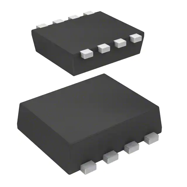
Package Dimensions
0.4
5
8
7
6
2.9
0.25
μA
0.9
V
8
V
1 : Emitter
2 : Emitter
3 : Emitter
4 : Gate
5 : Collector
6 : Collector
7 : Collector
8 : Collector
0.15
5
2.3
0 t o 0.02
2.8
±10
5
Top View
1
2
3
4
Top view
4
1
0.65
0.3
0.9
0.25
μA
Electrical Connection
unit : mm (typ)
7011A-004
8
10
0.07
1 : Emitter
2 : Emitter
3 : Emitter
4 : Gate
5 : Collector
6 : Collector
7 : Collector
8 : Collector
SANYO : ECH8
Bot t om View
Fig.1 Large Current R Load Switching Circuit
RL
CM
+
VCC
RG
TIG062E8
100kΩ
Note1. Gate Series Resistance RG ≥ 250Ω is recommended for protection purpose at the time of turn OFF. However,
if dv / dt ≤ 400V / μs is satisfied at customer’s actual set evaluation, RG < 250Ω can also be used.
Note2. The collector voltage gradient dv / dt must be smaller than 400V / μs to protect the device when it is turned off.
No. A1480-2/5
�TIG062E8
3.0V
2.5V
75
1.8V
50
0
1
2
3
4
5
6
7
8
9
Collector-to-Emitter Voltage, VCE -- V
VCE -- VGE
Collector-to-Emitter Voltage, VCE -- V
8
7
6
5
25°C
Tc=75°C
4
--25°C
3
2
1
2
3
4
5
6
Gate-to-Emitter Voltage, VGE -- V
IT14700
VCE(sat) -- Tc
Collector-to-Emitter
Saturation Voltage, VCE(sat) -- V
10
9
0A
15
I C=
4V,
=
V GE
8
7
A
6
00
I =1
=3V, C
VGE
5
4
3
2
--50
--25
0
25
50
100
75
125
Case Temperature, Tc -- °C
3
150
Tc
=
VCE -- VGE
IC=150A
8
Tc=75°C
25°C
--25°C
7
6
5
4
3
2
1
5
6
Gate-to-Emitter Voltage, VGE -- V
2
3
4
IT14701
VGE(off) -- Tc
0.9
VCE=10V
IC=1mA
0.8
0.7
0.6
0.5
0.4
0.3
0.2
0.1
--50
--25
0
25
50
75
Coes
Cres
100
125
Case Temperature, Tc -- °C
Switching Time, SW Time -- ns
2
2
3
Test circuit Fig.1
VGE=3V
VCC=320V
RG=250Ω
CM=150μF
PW=50μs
td(o
ff)
2
tf
1000
150
IT14703
SW Time -- ICP
3
3
3
5
IT14699
5
1000
7
5
100
7
5
2
9
1
f=1MHz
Cies
2
1
IT14702
Cies, Coes, Cres -- VCE
5
4
Gate-to-Emitter Voltage, VGE -- V
0
10
IC=100A
11
Cies, Coes, Cres -- pF
50
IT14698
9
10
7
75
0
10
Gate-to-Emitter Cutoff Voltage, VGE(off) -- V
Collector-to-Emitter Voltage, VCE -- V
10
1
100
25
25
0
75
°C
100
125
Collector Current, IC -- A
Collector Current, IC -- A
V
=4
GE
VCE=10V
25
°C
.0V
125
IC -- VGE
150
--2
5°
C
IC -- VCE
150
tr
7
5
3
td(on)
2
100
0
2
4
6
8
10
12
14
16
Collector-to-Emitter Voltage, VCE -- V
18
20
IT14704
7
10
2
3
5
7
100
2
Collector Current (Pulse), ICP -- A
3
5
IT14705
No. A1480-3/5
�TIG062E8
SW Time -- RG
5
tf
1000
7
ff)
t d(o
tr
5
3
2
)
on
t d(
100
Test circuit Fig.1
VGE=3V
VCC=320V
ICP=100A
CM=150μF
PW=50μs
7
5
2
3
5
7
2
100
3
5
Gate Series Resistance, RG -- Ω
ICP -- VGE
VCE=320V
CM=100μF
140
80
60
40
200
50
100
150
200
250
300
350
400
450
Gate Series Resistance, RG -- Ω
20
1
2
3
4
5
CM -- ICP2
300
500
IT14707
CM -- ICP1
200
100
VGE=3.3V
VCE=320V
60
80
100
Tc=70°C
150
100
50
VGE=3V
VCE=320V
0
20
40
120
Collector Current (Pulse)2, ICP2 -- A
140
160
IT14710
60
80
100
120
140
Collector Current (Pulse)1, ICP1 -- A
160
IT14709
CM -- ICP3
300
Tc=70°C
40
Tc=25°C
200
0
6
Tc=25°C
150
250
IT14708
250
20
300
300
Gate-to-Emitter Voltage, VGE -- V
Maximum Capacitor, CM -- μF
1000
IT14706
Tc=70°C
0
400
0
0
7
100
0
500
Tc=25°C
120
0
0
600
100
Maximum Capacitor, CM -- μF
Collector Current (Pulse), ICP -- A
160
Turn OFF, dv / dt -- V / μs
2
50
Test circuit Fig.1
VGE=3V
VCC=320V
ICP=100A
PW=50μs
700
Maximum Capacitor, CM -- μF
Switching Time, SW Time -- ns
3
3
2
dv / dt -- RG
800
250
Tc=25°C
200
Tc=70°C
150
100
50
0
VGE=4V
VCE=320V
0
20
40
60
80
100
120
140
Collector Current (Pulse)3, ICP3 -- A
160
IT14711
No. A1480-4/5
�TIG062E8
Note : TIG062E8 has protection diode between gate and emitter but handling it requires sufficient care
to be taken.
SANYO Semiconductor Co.,Ltd. assumes no responsibility for equipment failures that result from using
products at values that exceed, even momentarily, rated values (such as maximum ratings, operating
condition ranges, or other parameters) listed in products specifications of any and all SANYO Semiconductor
Co.,Ltd. products described or contained herein.
SANYO Semiconductor Co.,Ltd. strives to supply high-quality high-reliability products, however, any and all
semiconductor products fail or malfunction with some probability. It is possible that these probabilistic failures
or malfunction could give rise to accidents or events that could endanger human lives, trouble that could give
rise to smoke or fire, or accidents that could cause damage to other property. When designing equipment,
adopt safety measures so that these kinds of accidents or events cannot occur. Such measures include but
are not limited to protective circuits and error prevention circuits for safe design, redundant design, and
structural design.
In the event that any or all SANYO Semiconductor Co.,Ltd. products described or contained herein are
controlled under any of applicable local export control laws and regulations, such products may require the
export license from the authorities concerned in accordance with the above law.
No part of this publication may be reproduced or transmitted in any form or by any means, electronic or
mechanical, including photocopying and recording, or any information storage or retrieval system, or
otherwise, without the prior written consent of SANYO Semiconductor Co.,Ltd.
Any and all information described or contained herein are subject to change without notice due to
product/technology improvement, etc. When designing equipment, refer to the "Delivery Specification" for the
SANYO Semiconductor Co.,Ltd. product that you intend to use.
Information (including circuit diagrams and circuit parameters) herein is for example only; it is not guaranteed
for volume production.
Upon using the technical information or products described herein, neither warranty nor license shall be
granted with regard to intellectual property rights or any other rights of SANYO Semiconductor Co.,Ltd. or any
third party. SANYO Semiconductor Co.,Ltd. shall not be liable for any claim or suits with regard to a third
party's intellectual property rights which has resulted from the use of the technical information and products
mentioned above.
This catalog provides information as of October, 2009. Specifications and information herein are subject
to change without notice.
PS No. A1480-5/5
�


 工商网监
湘ICP备2023018690号
工商网监
湘ICP备2023018690号
