DATA SHEET
www.onsemi.com
NPN High-Power Transistors
TIP33C
Designed for general−purpose power amplifier and switching
applications.
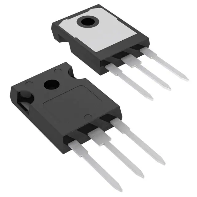
TO−247
CASE 340L
STYLE 3
Features
• ESD Ratings: Machine Model, C; > 400 V
•
•
Human Body Model, 3B; > 8000 V
Epoxy Meets UL 94 V−0 @ 0.125 in
These Devices is Pb−Free*
10 AMPERE
NPN SILICON
POWER TRANSISTORS
60 & 100 VOLT, 80 WATTS
MAXIMUM RATINGS
Rating
Symbol
Value
Unit
Collector − Emitter Voltage
VCEO
60
Vdc
Collector − Base Voltage
VCBO
60
Vdc
Emitter − Base Voltage
VEBO
5.0
Vdc
IC
10
15
Adc
Apk
Base Current − Continuous
IB
3.0
Adc
Total Device Dissipation @ TC = 25°C
Derate above 25°C
PD
80
0.64
Watts
W/°C
TJ, Tstg
– 65 to
+150
°C
Symbol
Max
Unit
Thermal Resistance, Junction−to−Case
RqJC
1.56
°C/W
Thermal Resistance, Junction−to−Ambient
RqJA
35.7
°C/W
Collector Current
− Continuous
− Peak (Note 1)
Operating and Storage Junction
Temperature Range
THERMAL CHARACTERISTICS
Characteristic
Stresses exceeding those listed in the Maximum Ratings table may damage the
device. If any of these limits are exceeded, device functionality should not be
assumed, damage may occur and reliability may be affected.
1. Pulse Test: Pulse Width v 300 ms, Duty Cycle v 2.0%.
MARKING DIAGRAM
TIP33C
AYWWG
1
BASE
TIP33C
A
Y
WW
G
3 EMITTER
2 COLLECTOR
=
=
=
=
=
Device Code
Assembly Location
Year
Work Week
Pb−Free Package
ORDERING INFORMATION
Device
Package
TIP33CG
TO−247
(Pb−Free)
Shipping†
30 Units / Rail
†For information on tape and reel specifications,
including part orientation and tape sizes, please
refer to our Tape and Reel Packaging Specifications
Brochure, BRD8011/D.
*For additional information on our Pb−Free strategy and soldering details, please
download the onsemi Soldering and Mounting Techniques Reference Manual,
SOLDERRM/D.
© Semiconductor Components Industries, LLC, 2012
September, 2022 − Rev. 5
1
Publication Order Number:
TIP33C/D
�TIP33C
ELECTRICAL CHARACTERISTICS (TC = 25_C unless otherwise noted)
Symbol
Min
Max
Unit
VCEO(sus)
60
−
−
Vdc
Collector−Emitter Cutoff Current
(VCE = 30 V, IB = 0) (VCE = 60 V, IB = 0)
ICEO
−
0.7
mA
Collector−Emitter Cutoff Current
(VCE = Rated VCEO, VEB = 0)
ICES
−
0.4
mA
Emitter−Base Cutoff Current
(VEB = 5.0 V, IC = 0)
IEBO
−
1.0
mA
40
20
−
100
−
−
1.0
4.0
−
−
1.6
3.0
Characteristic
OFF CHARACTERISTICS
Collector−Emitter Sustaining Voltage (Note 2) (IC = 30 mA, IB = 0)
ON CHARACTERISTICS (Note 2)
DC Current Gain
(IC = 1.0 A, VCE = 4.0 V)
(IC = 3.0 A, VCE = 4.0 V)
hFE
Collector−Emitter Saturation Voltage
(IC = 3.0 A, IB = 0.3 A)
(IC = 10 A, IB = 2.5 A)
VCE(sat)
Base−Emitter On Voltage
(IC = 3.0 A, VCE = 4.0 V)
(IC = 10 A, VCE = 4.0 V)
VBE(on)
−
Vdc
Vdc
DYNAMIC CHARACTERISTICS
Small−Signal Current Gain
(IC = 0.5 A, VCE = 10 V, f = 1.0 kHz)
hfe
20
−
−
Current−Gain — Bandwidth Product
(IC = 0.5 A, VCE = 10 V, f = 1.0 MHz)
fT
3.0
−
MHz
2. Pulse Test: Pulse Width v 300 ms, Duty Cycle v 2.0%.
www.onsemi.com
2
�TIP33C
500
VCE = 4.0 V
TJ = 25°C
hFE , DC CURRENT GAIN
200
100
50
20
NPN
PNP
10
5.0
0.1
10
1.0
IC, COLLECTOR CURRENT (A)
Figure 1. DC Current Gain
15
10
1.0�ms
5.0
3.0
2.0
1.0
0.5
0.2
0.1
1.0
10�ms
300�ms
dc
SECONDARY BREAKDOWN LIMIT
BONDING WIRE LIMIT
THERMAL LIMIT
TC = 25°C
TIP33A
IC, COLLECTOR CURRENT (AMPS)
IC, COLLECTOR CURRENT (AMPS)
20
TIP33C
2.0 3.0
5.0 7.0 10
20 30
50
VCE, COLLECTOR-EMITTER VOLTAGE (VOLTS)
L = 200 mH
IC/IB ≥ 5.0
VBE(off) = 0 to 5.0 V
TC = 100°C
15
10
5.0
0
70 100
0
Figure 2. Maximum Rated Forward Bias
Safe Operating Area
20
40
60
80
VCE, COLLECTOR-EMITTER VOLTAGE (VOLTS)
100
Figure 3. Maximum Rated Forward Bias
Safe Operating Area
FORWARD BIAS
REVERSE BIAS
The Forward Bias Safe Operating Area represents the
voltage and current conditions these devices can withstand
during forward bias. The data is based on TC = 25_C; TJ(pk)
is variable depending on power level. Second breakdown
pulse limits are valid for duty cycles to 10%, and must be
derated thermally for TC > 25_C.
The Reverse Bias Safe Operating Area represents the
voltage and current conditions these devices can withstand
during reverse biased turn−off. This rating is verified under
clamped conditions so the device is never subjected to an
avalanche mode.
www.onsemi.com
3
�MECHANICAL CASE OUTLINE
PACKAGE DIMENSIONS
TO−247
CASE 340L
ISSUE G
DATE 06 OCT 2021
SCALE 1:1
GENERIC
MARKING DIAGRAM*
XXXXXXXXX
AYWWG
STYLE 1:
PIN 1.
2.
3.
4.
GATE
DRAIN
SOURCE
DRAIN
STYLE 2:
PIN 1.
2.
3.
4.
ANODE
CATHODE (S)
ANODE 2
CATHODES (S)
STYLE 5:
PIN 1.
2.
3.
4.
CATHODE
ANODE
GATE
ANODE
STYLE 6:
PIN 1.
2.
3.
4.
MAIN TERMINAL 1
MAIN TERMINAL 2
GATE
MAIN TERMINAL 2
DOCUMENT NUMBER:
DESCRIPTION:
STYLE 3:
PIN 1.
2.
3.
4.
98ASB15080C
TO−247
BASE
COLLECTOR
EMITTER
COLLECTOR
STYLE 4:
PIN 1.
2.
3.
4.
GATE
COLLECTOR
EMITTER
COLLECTOR
XXXXX
A
Y
WW
G
= Specific Device Code
= Assembly Location
= Year
= Work Week
= Pb−Free Package
*This information is generic. Please refer to
device data sheet for actual part marking.
Pb−Free indicator, “G” or microdot “G”, may
or may not be present. Some products may
not follow the Generic Marking.
Electronic versions are uncontrolled except when accessed directly from the Document Repository.
Printed versions are uncontrolled except when stamped “CONTROLLED COPY” in red.
PAGE 1 OF 1
onsemi and
are trademarks of Semiconductor Components Industries, LLC dba onsemi or its subsidiaries in the United States and/or other countries. onsemi reserves
the right to make changes without further notice to any products herein. onsemi makes no warranty, representation or guarantee regarding the suitability of its products for any particular
purpose, nor does onsemi assume any liability arising out of the application or use of any product or circuit, and specifically disclaims any and all liability, including without limitation
special, consequential or incidental damages. onsemi does not convey any license under its patent rights nor the rights of others.
© Semiconductor Components Industries, LLC, 2021
www.onsemi.com
�onsemi,
, and other names, marks, and brands are registered and/or common law trademarks of Semiconductor Components Industries, LLC dba “onsemi” or its affiliates
and/or subsidiaries in the United States and/or other countries. onsemi owns the rights to a number of patents, trademarks, copyrights, trade secrets, and other intellectual property.
A listing of onsemi’s product/patent coverage may be accessed at www.onsemi.com/site/pdf/Patent−Marking.pdf. onsemi reserves the right to make changes at any time to any
products or information herein, without notice. The information herein is provided “as−is” and onsemi makes no warranty, representation or guarantee regarding the accuracy of the
information, product features, availability, functionality, or suitability of its products for any particular purpose, nor does onsemi assume any liability arising out of the application or use
of any product or circuit, and specifically disclaims any and all liability, including without limitation special, consequential or incidental damages. Buyer is responsible for its products
and applications using onsemi products, including compliance with all laws, regulations and safety requirements or standards, regardless of any support or applications information
provided by onsemi. “Typical” parameters which may be provided in onsemi data sheets and/or specifications can and do vary in different applications and actual performance may
vary over time. All operating parameters, including “Typicals” must be validated for each customer application by customer’s technical experts. onsemi does not convey any license
under any of its intellectual property rights nor the rights of others. onsemi products are not designed, intended, or authorized for use as a critical component in life support systems
or any FDA Class 3 medical devices or medical devices with a same or similar classification in a foreign jurisdiction or any devices intended for implantation in the human body. Should
Buyer purchase or use onsemi products for any such unintended or unauthorized application, Buyer shall indemnify and hold onsemi and its officers, employees, subsidiaries, affiliates,
and distributors harmless against all claims, costs, damages, and expenses, and reasonable attorney fees arising out of, directly or indirectly, any claim of personal injury or death
associated with such unintended or unauthorized use, even if such claim alleges that onsemi was negligent regarding the design or manufacture of the part. onsemi is an Equal
Opportunity/Affirmative Action Employer. This literature is subject to all applicable copyright laws and is not for resale in any manner.
PUBLICATION ORDERING INFORMATION
LITERATURE FULFILLMENT:
Email Requests to: orderlit@onsemi.com
onsemi Website: www.onsemi.com
◊
TECHNICAL SUPPORT
North American Technical Support:
Voice Mail: 1 800−282−9855 Toll Free USA/Canada
Phone: 011 421 33 790 2910
Europe, Middle East and Africa Technical Support:
Phone: 00421 33 790 2910
For additional information, please contact your local Sales Representative
�


 工商网监
湘ICP备2023018690号
工商网监
湘ICP备2023018690号

