TM
Application Specific Crystal Oscillator 7.0 x 5.0mm
3.3V CMOS Low-Jitter 25 MHz GbE XO
FNETHE025
7.0 x 5.0mm Ceramic SMD
ASSP XO™ for Networking
Package:
Product Features
• Very low Pk to Pk jitter - 50ps Max • Low output current - 15mA Max • Low power standby mode • RoHS Compliant
Recommended Land Pattern:
Product Description
This is an enhanced 3.3V, 25MHz crystal clock oscillator with superb jitter and low operating current for providing clock references in Gigabit Ethernet applications.
Applications
• Gigabit Ethernet Switch
Pin Functions:
Pin Function
1 2 3 4
OE Function Ground Clock Output V DD
*Extended high frequency power decoupling is recommended (see test circuit for minimum recommendation). To ensure optimal performance, do not route RF traces beneath the package.
Part Ordering Information:
FNETHE025
SaRonix-eCera™ is a Pericom® Semiconductor company
•
US: +1-408-435-0800 TW: +886-3-4518888 10-0020
•
www.pericom.com 04/13/10 1
A ll specifications are subject to change without notice.
FNETHE025
Rev E
�3.3V CMOS Low-Jitter 25 MHz GbE XO FNETHE025
TM
Application Specific Crystal Oscillator 7.0 x 5.0mm
Electrical Performance
Parameter Min. Typ. Max. Units Notes
Output Frequency Supply Voltage V DD Supply Current, Output Enabled Supply Current, Output Disabled Frequency Stability Operating Temperature Range Output Logic 0, VOL Output Logic 1, VOH Output Load Duty Cycle Rise and Fall Time Jitter, pk-pk 45 90% V DD -20 2.97
25 3.3 3.63 15 10 ±25 +70 10% V DD 15 55 7 50
MHz V mA µA ppm °C V V pF % ns ps Measured 50% V DD Measured 20/80% of waveform 100.000 random periods See Note 1 below
Notes: 1. Stability includes all combinations of operating temperature, load changes, rated input (supply) voltage changes, initial calibration tolerance (25°C), aging (1 year at 25°C average effective ambient temperature), shock and vibration. 2. For specifications othere than those listed, please contact sales.
Output Enable / Disable Function
Parameter Min. Typ. Max. Units Notes
Input Voltage (pin 1), Output Enable Input Voltage (pin 1), Output Disable (low power standby) Internal Pullup Resistance Output Disable Delay Output Enable Delay
0.7 V DD 0.3 V DD 30 50 2
V V kΩ ns ms
or open Output is Hi-Z
Absolute Maximum Ratings
Parameter Min. Typ. Max. Units Notes
Storage Temperature
-55
+125
°C
For the latest product information visit: http://www.pericom.com/products/timing/oscillators/FNETHE025/ For test circuit go to: http://www.pericom.com/pdf/sre/tc_hcmos.pdf For soldering reflow profile and reliability test ratings go to: http://www.pericom.com/pdf/sre/reflow.pdf For tape and reel information go to: http://www.pericom.com/pdf/sre/tr_7050.pdf
SaRonix-eCera™ is a Pericom® Semiconductor company
•
US: +1-408-435-0800 TW: +886-3-4518888 10-0020
•
www.pericom.com 04/13/10 2
A ll specifications are subject to change without notice.
FNETHE025
Rev E
�
很抱歉,暂时无法提供与“FNETHE025”相匹配的价格&库存,您可以联系我们找货
免费人工找货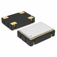


 工商网监
湘ICP备2023018690号
工商网监
湘ICP备2023018690号
