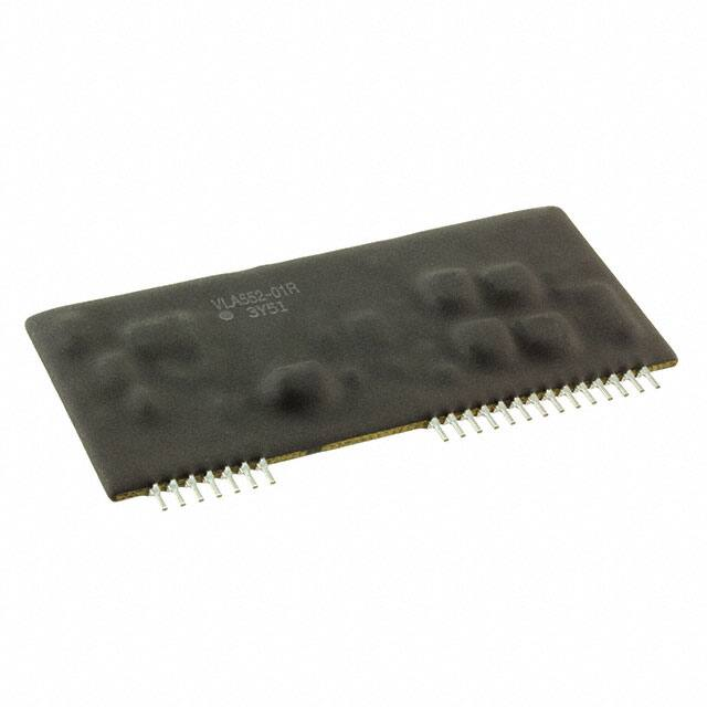
VLA552-01R
Powerex, Inc., 173 Pavilion Lane, Youngwood, Pennsylvania 15697 (724) 925-7272
www.pwrx.com
A
IGBT Gate Driver +
DC/DC Converter
C
B
J
K
E
D
H
D
30
1
DC-AC CONVERTER
1
VD 2
Gi 3
4
Vl+ 6
Vl - 7
120Ω
REGULATOR
LATCH
TIMER &
RESET CIRCUIT
1k
INTERFACE
120Ω
GATE
SHUTDOWN
CIRCUIT
OPTO
COUPLER
DETECT
CIRCUIT
F
G
19 VCC
29 ttrip CONTROL
30 DETECT PIN
20 GND
26 COLLECTOR
CLAMP ASSIST
25 VCC
23 VO
24
SHUTDOWN
27
SPEED CONTROL
28 FAULT OUTPUT
21 VEE
22
Pins 5, 17, 18 : NC
Circuit Diagram
Dimensions Inches Millimeters
A
3.46 Max.
88.0 Max.
B
1.67 Max.
42.5 Max.
C
0.67 Max.
17.0 Max.
D
0.31 Max.
8.0 Max.
E
0.1
2.54
F
0.45 Max.
11.5 Max.
G
0.24 Max.
6.0 Max.
H
0.03±0.004 0.75±0.1
J
0.14±0.04 3.5±1.0
K
0.028 Max.
0.7 Max.
07/14 Rev. 0
Description:
VLA552-01R is a hybrid
integrated circuit designed for
driving n-channel IGBT modules in
any gate-amplifier application. This
device is a fully isolated gate drive
circuit consisting of an optically
isolated gate drive amplifier and an
isolated DC-DC converter. The gate
driver provides an over-current
protection function based on
desaturation detection.
Features:
£ Built in Isolated DC-DC
Converter for Gate Drive
£ SIP Outline Allows More Space
£ Built in Short Circuit Protection
with a pin for Fault Output
£ Built in Collector Clamp Circuit
£ Variable Fall Time on ShortCircuit Protection
£ Electrical Isolation Voltage
4000 Vrms (for 1 Minute)
£ CMOS Compatible Input
Interface
Applications:
£ To Drive IGBT Modules for
General Industrial Use.
Recommended IGBT Modules:
VCES = 1200V Series up to
3600A Class
VCES = 1700V Series up to
3600A Class
1
�Powerex, Inc., 173 Pavilion Lane, Youngwood, Pennsylvania 15697 (724) 925-7272 www.pwrx.com
VLA552-01
IGBT Gate Driver + DC/DC Converter
Absolute Maximum Ratings, Ta = 25°C unless otherwise specified
Characteristics
Symbol Rating Units
Supply Voltage (DC)
Input Signal Voltage (Applied Between Pins 6-7, 50% Duty Cycle, Pulse Width 1ms)
Output Peak Current (Pulse Width 3μs)
VD
-1 ~ 16.5
Volts
VI
-7 ~ +7
Volts
IOHP -24 Amperes
IOLP 24 Amperes
Isolation Voltage (Sine Wave Voltage 60Hz, for 1 min., R.H. 60A Class
R1 : 1Ω, 1W Class
R2 : 10Ω, 1/4W Class
DZ3~6 : Vpn < Total VZ < VCES of IGBT
Rough guide of total VZ is as follows:
For VCES 1200V Series 900~1000V
For VCES 1700V Series 1300~1400V
It depends on Vpn, IC(max), RG, snubber
circuit inductance of power main circuit, and
kind of main condenser.
NOTE:
1. Decoupling capacitors should be located as close as possible to the Hybrid IC pins.
2. The gate circuit path should be kept as short as possible to minimize influence of switching noise.
3. D1 requires approximately the same blocking voltage as the IGBT modules.
4. When recovery current flows in D1, Pin 30 sees high voltage. A zener diode between Pin 21 and Pin 30 is necessary
as shown in above diagram.
5. If the short-circuit protection circuit is not used, please connect a 4.7k ohm resistor between Pin 30 and pin 20.
(D1 and DZ1 are not required.)
6. If the collector clamp circuit is activated repeatedly, it may be destroyed as a result of overheating. For this reason,
power dissipation of the zener diode should be determined by testing in the actual inverter.
07/14 Rev. 0
3
�Powerex, Inc., 173 Pavilion Lane, Youngwood, Pennsylvania 15697 (724) 925-7272 www.pwrx.com
VLA552-01
IGBT Gate Driver + DC/DC Converter
Operation of Protection Circuit
Adjustment of Output Fall Time
1. When an “ON” input signal is applied for a period longer than Ttrip
and the collector voltage is high, the hybrid IC will recognize the
condition as a short-circuit and immediately reduce the gate voltage.
It will also produce a low voltage fault signal at the respective Pin 29
or Pin 16 alerting that the protection circuit is in operation.
2. The protection circuit will reset if an “OFF” input signal is applied and
the minimum 1~2ms shutdown time has passed. “OFF” signal must
be 10μs or more.
3. The controlled time to detect a short-circuit (Ttrip) should be set so
that the IGBT can be fully turned “ON” before a short-circuit condition
can be detected. It is possible to adjust Ttrip by connecting a capacitor (Ctrip) between Pins 18 and 21, as well as Pins 27 and 24.
4. When the short-circuit protection is activated, the soft gate shutdown
circuit reduces the collector surge voltage on the IGBT. The gate shut
down speed can be slowed even more by adding a capacitor to the
CS terminal (between Pins 15 and 18; Pins 27 and 30).
INPUT
SIGNAL
90%
t2
t1
50%
10%
VO
0%
Operation Flow on Detecting Short Circuit
START
t1, t2 vs CS CHARACTERISTICS
(TYPICAL)
DETECTION OF
SHORT CIRCUIT
GATE SHUTDOWN
CIRCUIT OPERATE
TIMER START
OUTPUT FAULT SIGN
END OF TIMER
1 ~ 2ms
NO
YES
INPUT SIGN
IS “OFF”
NO
YES
CLEAR ALARM
ENABLE OUTPUT
FALL TIME ON ACTIVITY OF
SHORT CIRCUIT PROTECTION, t1, t2, (µs)
45
40
35
30
25
t2
20
15
10
t1
5
0
0
100 200 300 400 500 600 700 800
CONNECTIVE CAPACITANCE, CS, (pF)
PIN: 27 – 21
NOTE: Output voltage with protection
circuit operating is about -lVEEl + 2V
4
07/14 Rev. 0
�Powerex, Inc., 173 Pavilion Lane, Youngwood, Pennsylvania 15697 (724) 925-7272 www.pwrx.com
VLA552-01R
IGBT Gate Driver + DC/DC Converter
VCC, | VEE | -Ta CHARACTERISTICS
(TYPICAL)
VCC, | VEE | -IO CHARACTERISTICS
(TYPICAL)
24
18
16
14
12
18
16
14
12
10
10
8
8
6
6
-20
1.6
PROPAGATION DELAY TIME “L-H”, tPLH, (μs)
PROPAGATION DELAY TIME “H-L”, tPHL, (μs)
20
1.4
1.2
1.0
0
20
40
60
0.10
0.15
0.20
tPLH, tPHL-Ta CHARACTERISTICS
(TYPICAL)
tPLH, tPHL-VI CHARACTERISTICS
(TYPICAL)
1.6
VD = 15V
VIN = 5V
RG = 1Ω
Ta = 25°C
LOAD C = 1.6μF
0.4
tPLH
tPHL
0
20
40
60
AMBIENT TEMPERATURE, Ta, (°C)
07/14 Rev. 0
0.05
LOAD CURRENT, IO, (AMPERES)
(PIN: 19-21, 22)
0.6
0
-20
0
AMBIENT TEMPERATURE, Ta, (°C)
0.8
0.2
4
80
PROPAGATION DELAY TIME “L-H”, tPLH, (μs)
PROPAGATION DELAY TIME “H-L”, tPHL, (μs)
VCC, | VEE |, (VOLTS)
20
Ta = 25°C, DC LOAD
VD = 15.8V
VD = 15V
VD = 14.2V
22
VCC, | VEE |, (VOLTS)
22
24
VCC
| VEE |
VD = 15V
RG = 1Ω
f = 3kHz
D.F. = 50%
80
1.4
1.2
0.25
VD = 15V
RG = 1Ω
Ta = 25°C
LOAD C = 1.6μF
1.0
0.8
0.6
0.4
0.2
0
3.5
tPLH
tPHL
4.0
4.5
5.0
5.5
6.0
INPUT SIGNAL VOLTAGE, VI, (VOLTS)
5
�Powerex, Inc., 173 Pavilion Lane, Youngwood, Pennsylvania 15697 (724) 925-7272 www.pwrx.com
VLA552-01
IGBT Gate Driver + DC/DC Converter
ttrip-Ta CHARACTERISTICS
(TYPICAL)
6.0
CONTROLLED TIME DETECT
SHORT CIRCUIT, ttrip, (μs)
4.5
4.0
3.5
3.0
2.5
2.0
ttrip1 (Ctrip1 = 0pF)
ttrip2 (Ctrip2 = 10pF)
1.0
-20
0.6
0
20
40
60
5
4
3
2
0
25
50
75
100
AMBIENT TEMPERATURE, Ta, (°C)
CONNECTIVE CAPACITANCE, Ctrip, (pF)
(PIN: 29-21)
ID-IO CHARACTERISTICS
(TYPICAL)
VOH, | VOL | -Ta CHARACTERISTICS
(TYPICAL)
22
0.3
0.2
0.1
0
6
0
80
0.4
0
7
1
VD = 15V
Ta = 25°C
0.5
VD = 15V
Ta = 25°C
8
“H” OUTPUT VOLTAGE, VOH, (VOLTS)
“L” OUTPUT VOLTAGE, | VOL |, (VOLTS)
CONTROLLED TIME DETECT
SHORT CIRCUIT, ttrip1, ttrip2, (μs)
5.0
1.5
INPUT CURRENT, ID, (AMPERES)
9
VD = 15V
Rg = 1Ω
Load: C = 1.6μF
5.5
0.05
0.10
0.15
0.20
LOAD CURRENT, IO, (AMPERES
(PIN: 19-21, 22)
6
ttrip-Ctrip CHARACTERISTICS
(TYPICAL)
0.25
20
18
16
125
VD = 15V
RG = 1Ω
LOAD: C = 1.6μF
VOH
| VOL |
14
12
10
8
6
4
-20
0
20
40
60
80
AMBIENT TEMPERATURE, Ta, (°C)
07/14 Rev. 0
�Powerex, Inc., 173 Pavilion Lane, Youngwood, Pennsylvania 15697 (724) 925-7272 www.pwrx.com
VLA552-01R
IGBT Gate Driver + DC/DC Converter
η-Idrive CHARACTERISTICS
(TYPICAL)
80
20
VD = 15V
Ta = 25°C
70
18
16
VCC, | VEE |, (VOLTS)
EFFICIENCY, η, (%)
60
50
40
30
20
0
0.05
0.10
0.16
0.20
8
6
IO = 0.1A
Ta = 25°C
VCC
| VEE |
13
16
17
Idrive-Ta CHARACTERISTICS
(TYPICAL)
η-VD CHARACTERISTICS
(TYPICAL)
0.15
0.10
RG = 1Ω
LOAD: = C = 1.6μF
15V
16.5V
20
40
18
IO = 0.1A
Ta = 25°C
70
0
15
SUPPLY VOLTAGE, VD, (VOLTS)
75
0.05
14
GATE DRIVE CURRENT, Idrive, (AMPERES)
EFFICIENCY, η, (%)
GATE DRIVE CURRENT, Idrive, (AMPERES)
10
0
0.25
0.20
65
60
55
50
45
60
80
AMBIENT TEMPERATURE, Ta, (°C)
07/14 Rev. 0
12
2
0.25
0
14
4
10
0
VCC, | VEE | -VD CHARACTERISTICS
(TYPICAL)
100
40
13
14
15
16
17
18
SUPPLY VOLTAGE, VD, (VOLTS)
7
�


 工商网监
湘ICP备2023018690号
工商网监
湘ICP备2023018690号
