LNK623-626 LinkSwitch-CV Family
®
Energy-Efficient, Off-line Switcher with Accurate Primary-side Constant-Voltage (CV) Control
Product Highlights
Dramatically Simplifies CV Converters • Eliminates optocoupler and all secondary CV control circuitry • Eliminates bias winding supply – IC is self biasing Advanced Performance Features • Compensates for external component temperature variations • Very tight IC parameter tolerances using proprietary trimming technology • Continuous and/or discontinuous mode operation for design flexibility • Frequency jittering greatly reduces EMI filter cost • Even tighter output tolerances achievable with external resistor selection/trimming Advanced Protection/Safety Features • Auto-restart protection reduces delivered power by >95% for output short circuit and all control loop faults (open and shorted components) • Hysteretic thermal shutdown – automatic recovery reduces power supply returns from the field • Meets HV creepage requirements between Drain and all other pins, both on the PCB and at the package EcoSmart ® – Energy Efficient • No-load consumption 67% at 115 VAC/230 VAC and no-load input power is 5 W, Clampless designs are not practical and an external RCD or Zener clamp should be used. 4. Ensure that worst-case, high line, peak drain voltage is below the BVDSS specification of the internal MOSFET and ideally ≤650 V to allow margin for design variation. VOR (Reflected Output Voltage), is the secondary output plus output diode forward voltage drop that is reflected to the primary via the turns ratio of the transformer during the diode conduction time. The VOR adds to the DC bus voltage and the leakage spike to determine the peak drain voltage. Pulse Grouping Pulse grouping is defined as 6 or more consecutive pulses followed by two or more timing state changes. The effect of pulse grouping is increased output voltage ripple. This is shown on the right of Figure 11 where pulse grouping has caused an increase in the output ripple. To eliminate group pulsing verify that the feedback signal settles within 2.1 μs from the turn off of the internal MOSFET. A Zener diode in the clamp circuit may be needed to achieve the desired settling time. If the settling time is satisfactory, then a RC network across RLOWER (R6) of the feedback resistors is necessary. The value of R (R5 in the Figure 12) should be an order of magnitude greater than RLOWER and selected such that R×C = 32 μs where C is C5 in Figure 12.
Quick Design Checklist
As with any power supply design, all LinkSwitch-CV designs should be verified on the bench to make sure that component specifications are not exceeded under worst-case conditions.
5 D6 1N4148 4
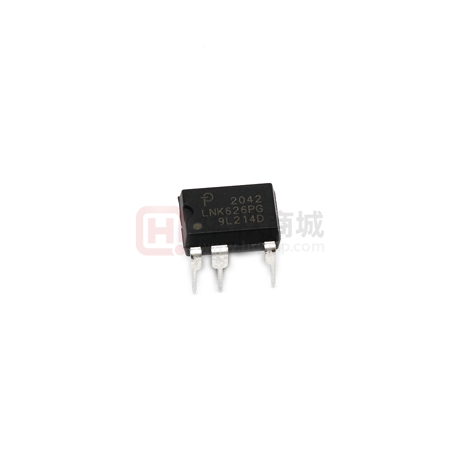
2 LinkSwitch-CV U1 LNK626PG
FB BP S
R3 6.34 k 1%
D
R4 6.2 k C4 1F 50 V
R5 47 k 1/8 W R6 4.02 k C5 1% 680 pF 50 V
C6 10 F 50 V
PI-5268-110608
Figure 12. RC Network Across RBOTTOM (R6) to Reduce Pulse Grouping.
Top Trace: Drain Waveform (200 V/div) Bottom Trace: Output Ripple Voltage (50 mV/div)
Split Screen with Bottom Screen Zoom Top Trace: Drain Waveform (200 V/div) Bottom Trace: Output Ripple Voltage (50 mV/div) Pulse Grouping (>5 Consecutive Switching Cycles).
Figure 11. Not Pulse Grouping ( VFBth FB Voltage = VFBth -0.1, Switch ON-Time = tON (MOSFET Switching at fOSC) VBP = 0 V VBP = 4 V LNK623/4 LNK625 LNK626 -5.0 -7.0 -4.0 -5.6 5.65 0.70 6.2 2.35 700 2.55 280 440 480 520 -3.4 -4.5 -2.3 -3.2 6.00 1.00 6.5 2.75 330 520 560 600 -1.8 -2.0 -1.0 -1.4 6.25 1.20 6.8 V V V mA μA ns μs
IS2
BYPASS Pin Charge Current
ICH1 ICH2
LNK623/4 LNK625/6 LNK623/4 LNK625/6
BYPASS Pin Voltage BYPASS Pin Voltage Hysteresis BYPASS Pin Shunt Voltage Circuit Protection
VBP VBPH VSHUNT
LNK623 di/dt = 50 mA/μs , TJ = 25 °C LNK624 di/dt = 60 mA/μs , TJ = 25 °C LNK625 di/dt = 80 mA/μs , TJ = 25 °C LNK626 di/dt = 110 mA/μs , TJ = 25 °C Leading Edge Blanking Time Thermal Shutdown Temperature Thermal Shutdown Hysteresis tLEB TSD TSDH TJ = 25 °C (See Note 3)
196 233 307 419 170 135
210 250 330 450 215 142 60
225 268 mA 353 482 ns 150 °C °C
Current Limit
ILIMIT
12
Rev. E 09/09
www.powerint.com
�LNK623-626
Parameter
Symbol
Conditions SOURCE = 0 V; TJ = -40 to 125 °C (Unless Otherwise Specified)
Min
Typ
Max
Units
Output LNK623 ID = 50 mA LNK624 ID = 50 mA RDS(ON) LNK625 ID = 62 mA LNK626 ID = 82 mA IDSS1 IDSS2 Breakdown Voltage DRAIN Supply Voltage Auto-Restart ON-Time Auto-Restart OFF-Time Open-Loop FB Pin Current Threshold Open-Loop ON-Time NOTES: 1. IDSS1 is the worst case OFF state leakage specification at 80% of BVDSS and maximum operating junction temperature. IDSS2 is a typical specification under worst case application conditions (rectified 265 VAC) for no-load consumption calculations. 2. When the duty cycle exceeds DCMAX the LinkSwitch-CV operates in on-time extension mode. 3. This parameter is derived from characterization. tAR-ON tAR-OFF IOL (See Note 3) (See Note 3) VFB = 0 (See Note 3) BVDSS TJ = 25 °C TJ = 100 °C TJ = 25 °C TJ = 100 °C TJ = 25 °C TJ = 100 °C TJ = 25 °C TJ = 100 °C 24 36 24 36 16 24 9.6 14 28 42 28 42 Ω 19 28 11 17 50 μA 15 700 50 200 2.5 -120 90 V V ms s μA μs
ON-State Resistance
OFF-State Leakage
VDS = 560 V (See Figure 20) TJ = 125 °C (See Note 1) VDS = 375 V (See Figure 20) TJ = 50 °C TJ = 25 °C (See Figure 20)
13
www.powerint.com
Rev. E 09/09
�LNK623-626
Typical Performance Characteristics
PI-5086-041008 PI-5089-040508
1.200 1.000 0.800 0.600 0.400 0.200 0.000 -40
1.200 1.000 0.800 0.600 0.400 0.200 0.000 -40
Frequency (Normalized to 25 °C)
Feedback Voltage (Normalized to 25 °C)
-15
10
35
60
85
110 135
-15
10
35
60
85
110 135
Temperature (°C)
Figure 13. Output Frequency vs, Temperature.
Temperature (°C)
Figure 14. Feedback Voltage vs, Temperature.
PI-2213-012301
Breakdown Voltage (Normalized to 25 °C)
250
Drain Current (mA)
TCASE=25 °C TCASE=100 °C
200 150 100 50
Scaling Factors: LNK623 1.0 LNK624 1.0 LNK625 1.5 LNK626 2.5
1.0
0.9 -50 -25 0 25 50 75 100 125 150
0 0 2 4 6 8 10
Junction Temperature ( °C)
Figure 15. Breakdown vs. Temperature.
DRAIN Voltage (V)
Figure 16. Output Characteristic.
PI-5201-071708
Drain Capacitance (pF)
40
Power (mW)
100
Scaling Factors: LNK623 1.0 LNK624 1.0 LNK625 1.5 LNK626 2.5
30
Scaling Factors: LNK623 1.0 LNK624 1.0 LNK625 1.5 LNK626 2.5
20
10
10
1 0 100 200 300 400 500 600
0 0 200 400 600
Drain Voltage (V)
Figure 17. COSS vs. Drain Voltage.
DRAIN Voltage (V)
Figure 18. Drain Capacitance Power.
14
Rev. E 09/09
www.powerint.com
PI-5212-080708
1000
50
PI-5211-080708
1.1
300
�LNK623-626
LinkSwitch-CV
FB BP S S S D S
VOUT
VIN +
+
10 F 6.2 V
500
+
2V
PI-5202-073108
1) Raise VBP voltage from 0 V to 6.2 V, down to 4.5 V, up to 6.2 V 2) Raise VIN until cycle skipping occurs at VOUT to measure VFBth 3) Apply 1.6 V at VIN and measure tFB delay from start of cycle falling edge to the next falling edge
Figure 19. Test Set-up for Feedback Pin Measurements.
LinkSwitch-CV
FB S S S D S
5F
50 k
10 k
1F .1 F
BP
4k VIN 16 V
+
S1
S2
Curve Tracer
To measure BVDSS, IDSS1, and IDSS2 follow these steps: 1) Close S1, open S2 2) Power-up VIN source (16 V) 3) Open S1, close S2 4) Measure I/V characteristics of Drain pin using the curve tracer Figure 20. Test Set-up for Leakage and Breakdown Tests.
PI-5203-071408
15
www.powerint.com
Rev. E 09/09
�LNK623-626
DIP-8C (P Package)
⊕D S
-E.004 (.10) Notes: 1. Package dimensions conform to JEDEC specification MS-001-AB (Issue B 7/85) for standard dual-in-line (DIP) package with .300 inch row spacing. 2. Controlling dimensions are inches. Millimeter sizes are shown in parentheses. 3. Dimensions shown do not include mold flash or other protrusions. Mold flash or protrusions shall not exceed .006 (.15) on any side. 4. Pin locations start with Pin 1, and continue counter-clockwise to Pin 8 when viewed from the top. The notch and/or dimple are aids in locating Pin 1. Pin 3 is omitted. 5. Minimum metal to metal spacing at the package body for the omitted lead location is .137 inch (3.48 mm). 6. Lead width measured at package body. 7. Lead spacing measured with the leads constrained to be perpendicular to plane T.
.240 (6.10) .260 (6.60)
Pin 1 -D.367 (9.32) .387 (9.83) .057 (1.45) .068 (1.73) (NOTE 6) .125 (3.18) .145 (3.68) .015 (.38) MINIMUM
-TSEATING PLANE .120 (3.05) .140 (3.56) .008 (.20) .015 (.38)
.100 (2.54) BSC .014 (.36) .022 (.56)
.048 (1.22) .053 (1.35)
.137 (3.48) MINIMUM
.300 (7.62) BSC (NOTE 7) .300 (7.62) .390 (9.91)
P08C
PI-3933-101507
⊕T E D
S .010 (.25) M
16
Rev. E 09/09
www.powerint.com
�LNK623-626
SO-8C
4
B
2 4.90 (0.193) BSC
0.10 (0.004) C A-B 2X
DETAIL A
A
8
4 5
D
GAUGE PLANE 2 3.90 (0.154) BSC 6.00 (0.236) BSC SEATING PLANE
C
1.04 (0.041) REF
0-8
o
0.25 (0.010) BSC
0.10 (0.004) C D 2X Pin 1 ID 1.27 (0.050) BSC 1 4 0.20 (0.008) C 2X 7X 0.31 - 0.51 (0.012 - 0.020) 0.25 (0.010) M C A-B D 1.25 - 1.65 (0.049 - 0.065) 0.10 (0.004) C 7X SEATING PLANE C
0.40 (0.016) 1.27 (0.050)
1.35 (0.053) 1.75 (0.069) 0.10 (0.004) 0.25 (0.010)
DETAIL A
H
0.17 (0.007) 0.25 (0.010)
Reference Solder Pad Dimensions
+
Notes: 1. JEDEC reference: MS-012. 2. Package outline exclusive of mold flash and metal burr. 3. Package outline inclusive of plating thickness. 4. Datums A and B to be determined at datum plane H. 5. Controlling dimensions are in millimeters. Inch dimensions are shown in parenthesis. Angles in degrees.
PI-4526-040207
2.00 (0.079)
4.90 (0.193)
+
+
+
0.60 (0.024)
D07C
1.27 (0.050)
Part Ordering Information
• LinkSwitch Product Family • CV Series Number • Package Identifier P D G Blank LNK 625 D G - TL TL Plastic DIP Plastic SO-8 GREEN: Halogen Free and RoHS Compliant Standard Configurations Tape & Reel, 2.5 k pcs for D Package. Not available for P Package.
• Package Material • Tape & Reel and Other Options
17
www.powerint.com
Rev. E 09/09
�Revision B C D E
Notes Release data sheet Correction made to Figure 5 Introduced Max current limit when V DRAIN is below 400 V Introduced LNK626DG
Date 11/08 12/08 07/09 09/09
For the latest updates, visit our website: www.powerint.com
Power Integrations reserves the right to make changes to its products at any time to improve reliability or manufacturability. Power Integrations does not assume any liability arising from the use of any device or circuit described herein. POWER INTEGRATIONS MAKES NO WARRANTY HEREIN AND SPECIFICALLY DISCLAIMS ALL WARRANTIES INCLUDING, WITHOUT LIMITATION, THE IMPLIED WARRANTIES OF MERCHANTABILITY, FITNESS FOR A PARTICULAR PURPOSE, AND NON-INFRINGEMENT OF THIRD PARTY RIGHTS. Patent Information The products and applications illustrated herein (including transformer construction and circuits external to the products) may be covered by one or more U.S. and foreign patents, or potentially by pending U.S. and foreign patent applications assigned to Power Integrations. A complete list of Power Integrations patents may be found at www.powerint.com. Power Integrations grants its customers a license under certain patent rights as set forth at http://www.powerint.com/ip.htm. Life Support Policy POWER INTEGRATIONS PRODUCTS ARE NOT AUTHORIZED FOR USE AS CRITICAL COMPONENTS IN LIFE SUPPORT DEVICES OR SYSTEMS WITHOUT THE EXPRESS WRITTEN APPROVAL OF THE PRESIDENT OF POWER INTEGRATIONS. As used herein: 1. A Life support device or system is one which, (i) is intended for surgical implant into the body, or (ii) supports or sustains life, and (iii) whose failure to perform, when properly used in accordance with instructions for use, can be reasonably expected to result in significant injury or death to the user. 2. A critical component is any component of a life support device or system whose failure to perform can be reasonably expected to cause the failure of the life support device or system, or to affect its safety or effectiveness. The PI logo, TOPSwitch, TinySwitch, LinkSwitch, DPA-Switch, PeakSwitch, EcoSmart, Clampless, E-Shield, Filterfuse, StakFET, PI Expert and PI FACTS are trademarks of Power Integrations, Inc. Other trademarks are property of their respective companies. ©2008, Power Integrations, Inc.
Power Integrations Worldwide Sales Support Locations
World Headquarters 5245 Hellyer Avenue San Jose, CA 95138, USA. Main: +1-408-414-9200 Customer Service: Phone: +1-408-414-9665 Fax: +1-408-414-9765 e-mail: usasales@powerint.com China (Shanghai) Room 1601/1610, Tower 1 Kerry Everbright City No. 218 Tianmu Road West Shanghai, P.R.C. 200070 Phone: +86-21-6354-6323 Fax: +86-21-6354-6325 e-mail: chinasales@powerint.com Germany Rueckertstrasse 3 D-80336, Munich Germany Phone: +49-89-5527-3910 Fax: +49-89-5527-3920 e-mail: eurosales@powerint.com India #1, 14th Main Road Vasanthanagar Bangalore-560052 India Phone: +91-80-4113-8020 Fax: +91-80-4113-8023 e-mail: indiasales@powerint.com Italy Via De Amicis 2 20091 Bresso MI Italy Phone: +39-028-928-6000 Fax: +39-028-928-6009 e-mail: eurosales@powerint.com Japan Kosei Dai-3 Bldg. 2-12-11, Shin-Yokohama, Kohoku-ku Yokohama-shi Kanagwan 222-0033 Japan Phone: +81-45-471-1021 Fax: +81-45-471-3717 e-mail: japansales@powerint.com Korea RM 602, 6FL Korea City Air Terminal B/D, 159-6 Samsung-Dong, Kangnam-Gu, Seoul, 135-728, Korea Phone: +82-2-2016-6610 Fax: +82-2-2016-6630 e-mail: koreasales@powerint.com Taiwan 5F, No. 318, Nei Hu Rd., Sec. 1 Nei Hu Dist. Taipei, Taiwan 114, R.O.C. Phone: +886-2-2659-4570 Fax: +886-2-2659-4550 e-mail: taiwansales@powerint.com Europe HQ 1st Floor, St. James’s House East Street, Farnham Surrey GU9 7TJ United Kingdom Phone: +44 (0) 1252-730-141 Fax: +44 (0) 1252-727-689 e-mail: eurosales@powerint.com Applications Hotline World Wide +1-408-414-9660
China (Shenzhen) Rm A, B & C 4th Floor, Block C, Electronics Science and Technology Bldg., 2070 Shennan Zhong Rd, Shenzhen, Guangdong, China, 518031 Phone: +86-755-8379-3243 Fax: +86-755-8379-5828 e-mail: chinasales@powerint.com
Singapore 51 Newton Road Applications Fax #15-08/10 Goldhill Plaza World Wide +1-408-414-9760 Singapore, 308900 Phone: +65-6358-2160 Fax: +65-6358-2015 e-mail: singaporesales@powerint.com
�


 工商网监
湘ICP备2023018690号
工商网监
湘ICP备2023018690号

