SAW Components
Data Sheet B3731
�SAW Components
B3731
Low-loss Filter
315,00 MHz
Data Sheet
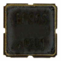
Ceramic package DCC6E
Features
0,6
2
3
5
1,5
■
■
■
■
■
6
(SMT)
Balanced and unbalanced operation possible
Passivation layer: Elpas
AEC-Q200 qualified component family
Compliant to EU RoHs Directive (2002/95/EC)
Lead free soldering compatible with J - STD20C
bottom view
1,0
■ RF low-loss filter for remote control receivers
■ Package for Surface Mounted Technology
side view
3,0
1,5
1
top view
4
1,8
3,0
Terminals
typ. dimensions in mm, approx. weight 0,037 g
■ Ni, gold plated
Pin configuration1)
1
2
4
5
3,6
Input (recommended) or Input Ground
Input Ground (recommended) or Input
Output (recommended) or Output Ground
Output Ground (recommended) or Output
to be grounded
Type
Ordering code
B3731
B39321-B3731-H110
Marking and package
according to
C61157-A7-A143
Packing
according to
F61074-V8168-Z000
Electrostactic Sensitive Device (ESD)
Maximum ratings
Operable temperature range TA
Storage temperature range Tstg
VDC
DC voltage
Source power
PS
1) The
–45/+120
–45/+120
6
10
˚C
˚C
V
dBm
source impedance 50 Ω
recommended pin configuration usually offers best suppression of electrical crosstalk.The
filter characteristics refer to this configuration.
2
Nov 14, 2005
�SAW Components
B3731
Low-loss Filter
315,00 MHz
Data Sheet
Characteristics
TA = –45 ... +95˚C
ZS = 50 Ω and matching network t.b.d.
ZL = 50 Ω and matching network t.b.d.
Reference temperature:
Terminating source impedance:
Terminating load impedance:
Center frequency
(center frequency between 3 dB points)
fC
Minimum insertion attenuation
including loss in matching elements (QL = 42)
excluding loss in matching elements
αmin
Pass band (relative to αmin)
314,85 ... 315,15 MHz
314,82 ... 315,18 MHz
314,78 ... 315,22 MHz
min.
typ.
max.
—
315,00
—
MHz
—
—
2,4
1,4
3.2
2,2
dB
dB
—
—
—
0,6
0,8
1,2
2,0
3,0
6,0
dB
dB
dB
0,57
0,63
0,69
MHz
48
43
32
25
10
38
42
52
60
55
53
48
36
29
14
43
46
57
65
60
—
—
—
—
—
—
—
—
—
—
dB
dB
dB
dB
dB
dB
dB
dB
dB
dB
—
610 || 2,2
610 || 2,2
—
Ω || pF
—
Ω || pF
Filter bandwidth
αrel≤ 3 dB
Relative attenuation (relative to αmin)
10,00 ... 295,00
295,00 ... 307,00
307,00 ... 312,00
312,00 ... 314,00
316,00 ... 325,00
325,00 ... 336,00
336,00 ... 370,00
370,00 ... 600,00
600,00 ...1500,00
1500,00 ...2500,00
αrel
MHz
MHz
MHz
MHz
MHz
MHz
MHz
MHz
MHz
MHz
Impedance for pass band matching 1)
Input: ZIN = RIN || CIN
Output: ZOUT = ROUT || COUT
—
1)
Impedance for passband matching bases on an ideal, perfect matching of the SAW filter to
source- and to load impedance (here 50 Ohm). After the SAW filter is removed and input impedance into the input matching / output matching network is calculated.
The conjugate complex value of these characteristic impedances are the input and output impedances for flat passband. For more details, we refer to EPCOS application note #4.
3
Nov 14, 2005
�SAW Components
B3731
Low-loss Filter
315,00 MHz
Data Sheet
Matching network to 50 Ω (element values depend on pcb layout and equivalent circuit)
Cp1 = 2,7 pF
Ls2 = 82 nH
Ls3 = 82 nH
Cp4 = 2,7 pF
Minimising the crosstalk
For a good ultimate rejection a low crosstalk is necessary. Low crosstalk can be realised with
a good RF layout. The major crosstalk mechanism is caused by the “ground-loop” problem.
Grounding loops are created if input-and output transducer GND are connected on the top-side
of the PCB and fed to the system grounding plane by a common via hole. To avoid the common
ground path, the ground pin of the input- and output transducer are fed to the system ground
plane (bottom PCB plane) by their own via hole. The transducers’ grounding pins should be
isolated from the upper grounding plane.
A common GND inductivity of 0.5nH degrades the ultimate rejection (crosstalk) by 20dB.
The optimised PCB layout, including matching network for transformation to 50 Ohm, is shown
here. In this PCB layout the grounding loops are minimised to realise good ultimate rejection.
Optimised PCB layout for SAW filters in DCC6E package, pinning 1,4 (top side, scale 1:1)
The bottom side is a copper plane (system ground area). The input and output grounding pins
are isolated and connected to the common ground by separated via holes.
For good contact of the upper grounding area with the lower side it is necessary to place
enough via holes.
4
Nov 14, 2005
�SAW Components
B3731
Low-loss Filter
315,00 MHz
Data Sheet
Frequency response
Frequency response (wideband)
5
Nov 14, 2005
�SAW Components
B3731
Low-loss Filter
315,00 MHz
Data Sheet
Frequency response (ultimate rejection)
Published by EPCOS AG
Surface Acoustic Wave Components Division, SAW CE AE PD
P.O. Box 80 17 09, D-81617 München
EPCOS AG 2005. All Rights Reserved. Reproduction, publication and dissemination of this brochure and the information contained therein without EPCOS’ prior express consent is prohibited.
The information contained in this brochure describes the type of component and shall not be considered as guaranteed characteristics. Purchase orders are subject to the General Conditions for
the Supply of Products and Services of the Electrical and Electronics Industry recommended by the
ZVEI (German Electrical and Electronic Manufacturers’ Association), unless otherwise agreed.
This brochure replaces the previous edition.
For questions on technology, prices and delivery please contact the Sales Offices of EPCOS AG or
the international Representatives.
Due to technical requirements components may contain dangerous substances. For information on
the type in question please also contact one of our Sales Offices.
6
Nov 14, 2005
�


 工商网监
湘ICP备2023018690号
工商网监
湘ICP备2023018690号
