CMOS SyncFIFO™
64 x 8, 256 x 8,
512 x 8, 1,024 x 8,
2,048 x 8 and 4,096 x 8
LEAD FINISH (SnPb) ARE IN EOL PROCESS - LAST TIME BUY EXPIRES JUNE 15, 2018
FEATURES:
•
•
•
•
•
•
•
•
•
•
•
•
•
•
•
•
IDT72420
IDT72200
IDT72210
IDT72220
IDT72230
IDT72240
DESCRIPTION:
64 x 8-bit organization (IDT72420)
256 x 8-bit organization (IDT72200)
512 x 8-bit organization (IDT72210)
1,024 x 8-bit organization (IDT72220)
2,048 x 8-bit organization (IDT72230)
4,096 x 8-bit organization (IDT72240)
10 ns read/write cycle time (IDT72420/72200/72210/72220/72230/
72240)
Read and Write Clocks can be asynchronous or coincidental
Dual-Ported zero fall-through time architecture
Empty and Full flags signal FIFO status
Almost-Empty and Almost-Full flags set to Empty+7 and Full-7,
respectively
Output enable puts output data bus in high-impedance state
Produced with advanced submicron CMOS technology
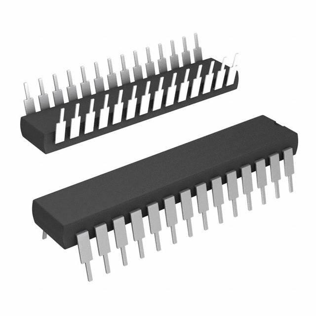
Available in 28-pin 300 mil plastic DIP
For surface mount product please see the IDT72421/72201/72211/
72221/72231/72241 data sheet
Green parts available, see ordering information
The IDT72420/72200/72210/72220/72230/72240 SyncFIFO™ are very
high-speed, low-power First-In, First-Out (FIFO) memories with clocked read
and write controls. These devices have a 64, 256, 512, 1,024, 2,048, and 4,096
x 8-bit memory array, respectively. These FIFOs are applicable for a wide
variety of data buffering needs, such as graphics, Local Area Networks (LANs),
and interprocessor communication.
These FIFOs have 8-bit input and output ports. The input port is controlled
by a free-running clock (WCLK), and a Write Enable pin (WEN). Data is written
into the Synchronous FIFO on every clock when WEN is asserted. The output
port is controlled by another clock pin (RCLK) and a Read Enable pin (REN).
The Read Clock can be tied to the Write Clock for single clock operation or the
two clocks can run asynchronous of one another for dual clock operation. An
Output Enable pin (OE) is provided on the read port for three-state control of
the output.
These Synchronous FIFOs have two endpoint flags, Empty (EF) and Full
(FF). Two partial flags, Almost-Empty (AE) and Almost-Full (AF), are provided
for improved system control. The partial (AE) flags are set to Empty+7 and Full7 for AE and AF respectively.
These FIFOs are fabricated using high-speed submicron CMOS technology.
FUNCTIONAL BLOCK DIAGRAM
D0 - D7
WCLK
WEN
INPUT REGISTER
EF
AE
AF
FF
FLAG
LOGIC
WRITE CONTROL
LOGIC
RAM ARRAY
64 x 8, 256 x 8,
512 x 8, 1,024 x 8,
2,048 x 8, 4,096 x 8
WRITE POINTER
READ POINTER
READ CONTROL
LOGIC
OUTPUT REGISTER
RESET LOGIC
RCLK
RS
REN
OE
2680 drw01
Q0 - Q7
IDT and the IDT logo are registered trademarks of Integrated Device Technology, Inc. The SyncFIFO is a trademark of Integrated Device Technology, Inc.
COMMERCIAL TEMPERATURE RANGE
FEBRUARY 2018
1
©2018 Integrated Device Technology, Inc. All rights reserved. Product specifications subject to change without notice.
DSC-2680/7
�IDT72420/72200/72210/72220/72230/72240 CMOS SYNCFIFO™
64 x 8, 256 x 8, 512 x 8, 1,024 x 8, 2,048 x 8, 4,096 x 8
COMMERCIAL TEMPERATURE RANGE
PIN CONFIGURATION
D4
1
28
D5
D3
2
27
D6
D2
3
26
D7
D1
4
25
RS
D0
5
24
WEN
AF
6
23
WCLK
AE
7
22
VCC
GND
8
21
Q7
RCLK
9
20
Q6
REN
10
19
Q5
OE
11
18
Q4
EF
12
17
Q3
FF
13
16
Q2
Q0
14
15
Q1
2680 drw02
PLASTIC THIN DIP (P28-2, order code: TP)
TOP VIEW
PIN DESCRIPTIONS
Symbol
D0 - D7
Name
Data Inputs
I/O
I
RS
Reset
I
Description
Data inputs for a 8-bit bus.
When RS is set LOW, internal read and write pointers are set to the first location of the RAM array, FF and AF go
HIGH, and AE and EF go LOW. A reset is required before an initial WRITE after power-up.
WCLK
Write Clock
I
Data is written into the FIFO on a LOW-to-HIGH transition of WCLK when WEN is asserted.
WEN
Write Enable
I
When WEN is LOW, data is written into the FIFO on every LOW-to-HIGH transition of WCLK. Data will not be written
into the FIFO if the FF is LOW.
Q0 - Q7
Data Outputs
O
Data outputs for a 8-bit bus.
RCLK
Read Clock
I
Data is read from the FIFO on a LOW-to-HIGH transition of RCLK when REN is asserted.
REN
Read Enable
I
When REN is LOW, data is read from the FIFO on every LOW-to-HIGH transition of RCLK. Data will not be read from
the FIFO if the EF is LOW.
OE
Output Enable
I
When OE is LOW, the data output bus is active. If OE is HIGH, the output data bus will be in a high-impedance
state.
EF
Empty Flag
O
When EF is LOW, the FIFO is empty and further data reads from the output are inhibited. When EF is HIGH, the FIFO
is not empty. EF is synchronized to RCLK.
AE
Almost-Empty Flag
O
When AE is LOW, the FIFO is almost empty based on the offset Empty+7. AE is synchronized to RCLK.
AF
Almost-Full Flag
O
When AF is LOW, the FIFO is almost full based on the offset Full-7. AF is synchronized to WCLK.
FF
Full Flag
O
When FF is LOW, the FIFO is full and further data writes into the input are inhibited. When FF is HIGH, the FIFO is not
full. FF is synchronized to WCLK.
VCC
Power
One +5 volt power supply pin.
GND
Ground
One 0 volt ground pin.
2
�IDT72420/72200/72210/72220/72230/72240 CMOS SYNCFIFO™
64 x 8, 256 x 8, 512 x 8, 1,024 x 8, 2,048 x 8, 4,096 x 8
COMMERCIAL TEMPERATURE RANGE
ABSOLUTE MAXIMUM RATINGS(1)
Symbol
VTERM
TSTG
Rating
Terminal Voltage with
Respect to GND
Storage Temperature
IOUT
DC Output Current
Com'l & Ind'l
–0.5 to +7.0
Unit
V
–55 to +125
°C
–50 to +50
mA
RECOMMENDED OPERATING
CONDITIONS
Symbol
VCC
GND
VIH
NOTE:
VIL
1. Stresses greater than those listed under ABSOLUTE MAXIMUM RATINGS may cause
permanent damage to the device. This is a stress rating only and functional operation of
the device at these or any other conditions above those indicated in the operational
sections of this specification is not implied. Exposure to absolute maximum rating
conditions for extended periods may affect reliability.
TA
Parameter
Supply Voltage
Commercial
Supply Voltage
Input High Voltage
Commercial
Input Low Voltage
Commercial
Operating Temperature
Commercial
Min.
4.5
Typ. Max.
5.0
5.5
Unit
V
0
2.0
0
—
0
—
V
V
—
—
0.8
V
0
—
70
°C
DC ELECTRICAL CHARACTERISTICS
(Commercial: VCC = 5V ± 10%, TA = 0°C to +70°C)
Symbol
Parameter
Min.
IDT72420
IDT72200
IDT72210
IDT72220
IDT72230
IDT72240
Commercial
tCLK = 10, 15, 25 ns
Typ.
Max.
Unit
ILI(1)
Input Leakage Current (any input)
–1
—
1
μA
ILO(2)
Output Leakage Current
–10
—
10
μA
VOH
Output Logic “1” Voltage, IOH = –2 mA
2.4
—
—
V
VOL
Output Logic “0” Voltage, IOL = 8 mA
—
—
0.4
V
I CC1(3,4,5)
Active Power Supply Current
—
—
40
mA
I CC2
Standby Current
—
—
5
mA
(3,6)
NOTES:
1. Measurements with 0.4 ≤ VIN ≤ VCC.
2. OE ≥ VIH, 0.4 ≤ VOUT ≤ VCC.
3. Tested with outputs open (IOUT = 0).
4. RCLK and WCLK toggle at 20 MHz and data inputs switch at 10 MHz.
5. Typical ICC1 = 1.7 + 0.7*fS + 0.02*CL*fS (in mA).
These equations are valid under the following conditions:
VCC = 5V, TA = 25°C, fS = WCLK frequency = RCLK frequency (in MHz, using TTL levels), data switching at fS/2, CL = capacitive load (in pF).
6. All Inputs = VCC - 0.2V or GND + 0.2V, except RCLK and WCLK, which toggle at 20 MHz.
3
�IDT72420/72200/72210/72220/72230/72240 CMOS SYNCFIFO™
64 x 8, 256 x 8, 512 x 8, 1,024 x 8, 2,048 x 8, 4,096 x 8
COMMERCIAL TEMPERATURE RANGE
AC ELECTRICAL CHARACTERISTICS
(Commercial: VCC = 5V ± 10%, TA = 0°C to + 70°C)
Symbol
fS
Parameter
Clock Cycle Frequency
tA
Data Access Time
tCLK
tCLKH
IDT72420L10
IDT72200L10
IDT72210L10
IDT72220L10
IDT72230L10
IDT72240L10
Min.
Max.
—
100
Commercial
IDT72420L15
IDT72200L15
IDT72210L15
IDT72220L15
IDT72230L15
IDT72240L15
Min.
Max.
—
66.7
IDT72420L25
IDT72200L25
IDT72210L25
IDT72220L25
IDT72230L25
IDT72240L25
Min.
Max.
—
40
Unit
MHz
2
6.5
2
10
2
15
ns
Clock Cycle Time
10
—
15
—
25
—
ns
Clock High Time
4.5
—
6
—
10
—
ns
tCLKL
Clock Low Time
4.5
—
6
—
10
—
ns
tDS
Data Setup Time
3
—
4
—
6
—
ns
tDH
Data Hold Time
0.5
—
1
—
1
—
ns
tENS
Enable Setup Time
3
—
4
—
6
—
ns
tENH
Enable Hold Time
0.5
—
1
—
1
—
ns
tRS
Reset Pulse Width
10
—
15
—
15
—
ns
tRSS
Reset Setup Time
8
—
10
—
15
—
ns
tRSR
Reset Recovery Time
8
—
10
—
15
—
ns
tRSF
Reset to Flag and Output Time
—
10
—
15
—
25
ns
(1)
tOLZ
Output Enable to Output in Low-Z
0
—
0
—
0
—
ns
tOE
Output Enable to Output Valid
2
6
3
8
3
13
ns
tOHZ
Output Enable to Output in High-Z(2)
2
6
3
8
3
13
ns
tWFF
Write Clock to Full Flag
—
6.5
—
10
—
15
ns
tREF
Read Clock to Empty Flag
—
6.5
—
10
—
15
ns
tAF
Write Clock to Almost-Full Flag
—
6.5
—
10
—
15
ns
tAE
Read Clock to Almost-Empty Flag
—
6.5
—
10
—
15
ns
tSKEW1
Skew time between Read Clock & Write Clock for
Empty Flag & Full Flag
4
—
6
—
10
—
ns
tSKEW2
Skew time between Read Clock & Write Clock for
Almost-Empty Flag & Almost-Full Flag
10
—
15
—
18
—
ns
(2)
NOTES:
1. Pulse widths less than minimum values are not allowed.
2. Values guaranteed by design, not currently tested.
CAPACITANCE (TA = +25°C, f = 1.0 MHz)
Symbol
CIN
(2)
COUT (1, 2)
Parameter
Conditions
Max.
Unit
Input Capacitance
VIN = 0V
10
pF
VOUT = 0V
10
pF
Output Capacitance
5V
1.1KΩ
NOTES:
1. With output deselected. (OE ≥ VIH)
2. Characterized values, not currently tested.
D.U.T.
680Ω
AC TEST CONDITIONS
Input Pulse Levels
Input Rise/Fall Times
Input Timing Reference Levels
Output Reference Levels
Output Load
GND to 3.0V
3ns
1.5V
1.5V
See Figure 1
30pF*
2680 drw03
or equivalent circuit
Figure 1. Output Load
*Includes jig and scope capacitances.
4
�IDT72420/72200/72210/72220/72230/72240 CMOS SYNCFIFO™
64 x 8, 256 x 8, 512 x 8, 1,024 x 8, 2,048 x 8, 4,096 x 8
COMMERCIAL TEMPERATURE RANGE
SIGNAL DESCRIPTIONS
When all the data has been read from the FIFO, the Empty Flag (EF) will
go LOW, inhibiting further read operations. Once a valid write operation has
been accomplished, the Empty Flag (EF) will go HIGH after tREF and a valid
read can begin. Read Enable (REN) is ignored when the FIFO is empty.
INPUTS:
Data In (D0–D7) — Data inputs for 8-bit wide data.
OUTPUT ENABLE (OE) — When Output Enable (OE) is enabled (LOW),
the parallel output buffers receive data from the output register. When
Output Enable (OE) is disabled (HIGH), the Q output data bus is in a highimpedance state.
CONTROLS:
RESET (RS) — Reset is accomplished whenever the Reset (RS) input is
taken to a LOW state. During reset, both internal read and write pointers are
set to the first location. A reset is required after power up before a write
operation can take place. The Full Flag (FF) and Almost-Full Flag (AF) will
be reset to HIGH after tRSF. The Empty Flag (EF) and Almost-Empty Flag
(AE) will be reset to LOW after tRSF. During reset, the output register is
initialized to all zeros.
OUTPUTS:
FULL FLAG (FF) — The Full Flag (FF) will go LOW, inhibiting further write
operation, when the device is full. If no reads are performed after Reset
(RS), the Full Flag (FF) will go LOW after 64 writes for the IDT72420, 256
writes for the IDT72200, 512 writes for the IDT72210, 1,024 writes for the
IDT72220, 2,048 writes for the IDT72230, and 4,096 writes for the IDT72240.
The Full Flag (FF) is synchronized with respect to the LOW-to-HIGH
transition of the Write Clock (WCLK).
WRITE CLOCK (WCLK) — A write cycle is initiated on the LOW-to-HIGH
transition of the Write Clock (WCLK). Data setup and hold times must be met
in respect to the LOW-to-HIGH transition of the Write Clock. The Full Flag
(FF) and Almost-Full Flag (AF) are synchronized with respect to the LOWto-HIGH transition of the Write Clock.
The Write and Read Clocks can be asynchronous or coincident.
EMPTY FLAG (EF) — The Empty Flag (EF) will go LOW, inhibiting further
read operations, when the read pointer is equal to the write pointer,
indicating the device is empty.
The Empty Flag (EF) is synchronized with respect to the LOW-to-HIGH
transition of the Read Clock (RCLK).
WRITE ENABLE (WEN) — When Write Enable (WEN) is LOW, data can
be loaded into the input register and RAM array on the LOW-to-HIGH
transition of every Write Clock (WCLK). Data is stored in the RAM array
sequentially and independently of any on-going read operation.
When Write Enable (WEN) is HIGH, the input register holds the previous
data and no new data is allowed to be loaded into the register.
To prevent data overflow, the Full Flag (FF) will go LOW, inhibiting
further write operations. Upon the completion of a valid read cycle, the Full
Flag (FF) will go HIGH after tWFF, allowing a valid write to begin. Write
Enable (WEN) is ignored when the FIFO is full.
ALMOST-FULL FLAG (AF) — The Almost-Full Flag (AF) will go LOW when
the FIFO reaches the almost-full condition. If no reads are performed after
Reset (RS), the Almost-Full Flag (AF) will go LOW after 57 writes for the
IDT72420, 249 writes for the IDT72200, 505 writes for the IDT72210, 1,017
writes for the IDT72220, 2,041 writes for the IDT72230 and 4,089 writes for
the IDT72240.
The Almost-Full Flag (AF) is synchronized with respect to the LOW-toHIGH transition of the Write Clock (WCLK).
READ CLOCK (RCLK) — Data can be read on the outputs on the LOW-toHIGH transition of the Read Clock (RCLK). The Empty Flag (EF) and
Almost-Empty flag (AE) are synchronized with respect to the LOW-to-HIGH
transition of the Read Clock.
The Write and Read Clocks can be asynchronous or coincident.
ALMOST-EMPTY FLAG (AE) — The Almost-Empty Flag (AE) will go LOW
when the FIFO reaches the almost-empty condition. If no reads are
performed after Reset (RS), the Almost-Empty Flag (AE) will go HIGH after
8 writes for the IDT72420, IDT72200, IDT72210, IDT72220, IDT72230 and
IDT72240.
The Almost-Empty Flag (AE) is synchronized with respect to the LOWto-HIGH transition of the Read Clock (RCLK).
READ ENABLE (REN) — When Read Enable (REN) is LOW, data is read
from the RAM array to the output register on the LOW-to-HIGH transition of
the Read Clock (RCLK).
When Read Enable (REN) is HIGH, the output register holds the
previous data and no new data is allowed to be loaded into the register.
DATA OUTPUTS (Q0–Q7) — Data outputs for 8-bit wide data.
TABLE 1 — STATUS FLAGS
IDT72420
IDT72200
0
0
Number of Words in FIFO
IDT72210
IDT72220
0
IDT72230
IDT72240
FF
AF
AE
EF
0
0
H
H
L
L
0
1 to 7
1 to 7
1 to 7
1 to 7
1 to 7
1 to 7
H
H
L
H
8 to 56
8 to 248
8 to 504
8 to 1,016
8 to 2,040
8 to 4,088
H
H
H
H
57 to 63
249 to 255
505 to 511
1,017 to 1,023
2,041 to 2,047
4,089 to 4,095
H
L
H
H
64
256
512
1,024
2,048
4,096
L
L
H
H
5
�IDT72420/72200/72210/72220/72230/72240 CMOS SYNCFIFO™
64 x 8, 256 x 8, 512 x 8, 1,024 x 8, 2,048 x 8, 4,096 x 8
COMMERCIAL TEMPERATURE RANGE
tRS
RS
tRSS
tRSR
tRSS
tRSR
REN
WEN
tRSF
EF, AE
tRSF
FF, AF
tRSF
OE = 1(1)
Q0 - Q7
OE = 0
2680 drw 04
NOTES:
1. After reset, the outputs will be LOW if OE = 0 and three-state if OE = 1.
2. The Clocks (RCLK, WCLK) can be free-running during reset.
Figure 2. Reset Timing
tCLK
tCLKH
tCLKL
WCLK
tDS
tDH
D0 - D7
DATA IN VALID
tENS
tENH
NO OPERATION
WEN
tWFF
tWFF
FF
tSKEW1(1)
RCLK
REN
2680 drw 05
NOTE:
1. tSKEW1 is the minimum time between a rising RCLK edge and a rising WCLK edge for FF to change during the current clock cycle. If the time between the rising edge of RCLK and the
rising edge of WCLK is less than tSKEW1, then FF may not change state until the next WCLK edge.
Figure 3. Write Cycle Timing
6
�IDT72420/72200/72210/72220/72230/72240 CMOS SYNCFIFO™
64 x 8, 256 x 8, 512 x 8, 1,024 x 8, 2,048 x 8, 4,096 x 8
COMMERCIAL TEMPERATURE RANGE
tCLK
tCLKH
tCLKL
RCLK
tENS
tENH
NO OPERATION
REN
tREF
tREF
EF
tA
VALID DATA
Q0 - Q7
tOLZ
tOHZ
tOE
OE
tSKEW1
(1)
WCLK
WEN
2680 drw 06
NOTE:
1. tSKEW1 is the minimum time between a rising WCLK edge and a rising RCLK edge for EF to change during the current clock cycle. If the time between the rising edge of WCLK and the
rising edge of RCLK is less than tSKEW1, then EF may not change state until the next RCLK edge.
Figure 4. Read Cycle Timing
WCLK
tDS
D1
D0 (first valid write)
D0 - D7
D2
D3
tENS
WEN
(1)
tFRL
tSKEW1
RCLK
tREF
EF
tENS
REN
tA
tA
D0
Q0 - Q7
D1
tOLZ
tOE
OE
2680 drw 07
NOTE:
1. When tSKEW1 ≥ minimum specification, tFRL maximum = tCLK + tSKEW1
When tSKEW1 < minimum specification, tFRL maximum = 2tCLK + tSKEW1 or tCLK + tSKEW1
The Latency Timing apply only at the Empty Boundary (EF = LOW).
Figure 5. First Data Word Latency Timing
7
�IDT72420/72200/72210/72220/72230/72240 CMOS SYNCFIFO™
64 x 8, 256 x 8, 512 x 8, 1,024 x 8, 2,048 x 8, 4,096 x 8
COMMERCIAL TEMPERATURE RANGE
NO WRITE
NO WRITE
NO WRITE
WCLK
tSKEW1
tSKEW1
tDS
DATA WRITE
D0 - D7
tWFF
tWFF
tWFF
FF
tENS
tENS
WEN
RCLK
tENH
tENH
tENS
tENS
REN
tA
OE LOW
Q0 - Q7
tA
DATA READ
DATA IN OUTPUT REGISTER
NEXT DATA READ
2680 drw 08
Figure 6. Full Flag Timing
WCLK
tDS
tDS
DATA WRITE 1
D0 - D7
tENS
DATA WRITE 2
tENS
tENH
tENH
WEN
tFRL
(1)
tFRL
(1)
tSKEW1
tSKEW1
RCLK
tREF
tREF
tREF
EF
REN
OE
LOW
tA
Q0 - Q7
DATA READ
DATA IN OUTPUT REGISTER
2680 drw 09
NOTE:
1. When tSKEW1 ≥ minimum specification, tFRL maximum = tCLK + tSKEW1
When tSKEW1 < minimum specification, tFRL maximum = 2tCLK + tSKEW1 or tCLK + tSKEW1
The Latency Timing apply only at the Empty Boundary (EF = LOW).
Figure 7. Empty Flag Timing
8
�IDT72420/72200/72210/72220/72230/72240 CMOS SYNCFIFO™
64 x 8, 256 x 8, 512 x 8, 1,024 x 8, 2,048 x 8, 4,096 x 8
tCLKH
COMMERCIAL TEMPERATURE RANGE
tCLKL
(2)
WCLK
tENS
tENH
WEN
tAF
AF
Full - 8 words in FIFO
Full - 7 words in FIFO
tSKEW2(1)
tAF
RCLK
tENH
tENS
REN
2680 drw10
NOTES:
1. tSKEW2 is the minimum time between a rising RCLK edge and a rising WCLK edge for AF to change during the current clock cycle. If the time between the rising edge of RCLK and the
rising edge of WCLK is less than tSKEW2, then AF may not change state until the next WCLK edge.
2. If a write is performed on this rising edge of the Write Clock, there will be Full -7 words in the FIFO when AF goes LOW.
Figure 8. Almost Full Flag Timing
tCLKH
tCLKL
WCLK
tENS
tENH
WEN
Empty+8
AE
Empty+7
tSKEW2 (1)
tAE
tAE
(2)
RCLK
tENS
tENH
2680 drw 11
REN
NOTES:
1. tSKEW2 is the minimum time between a rising WCLK edge and a rising RCLK edge for AE to change during the current clock cycle. If the time between the rising edge of WCLK and the
rising edge of RCLK is less than tSKEW2, then AE may not change state until the next RCLK edge.
2. If a read is performed on this rising edge of the Read Clock, there will be Empty +7 words in the FIFO when AE goes LOW.
Figure 9. Almost Empty Flag Timing
9
�IDT72420/72200/72210/72220/72230/72240 CMOS SYNCFIFO™
64 x 8, 256 x 8, 512 x 8, 1,024 x 8, 2,048 x 8, 4,096 x 8
COMMERCIAL TEMPERATURE RANGE
OPERATING CONFIGURATIONS
SINGLE DEVICE CONFIGURATION - A single IDT72420/72200/72210/
72220/72230/72240 may be used when the application requirements are
for 64/256/512/1,024/2,048/4,096 words or less. See Figure 10.
RESET (RS)
WRITE CLOCK (WCLK)
READ CLOCK (RCLK)
WRITE ENABLE (WEN)
READ ENABLE (REN)
OUTPUT ENABLE (OE)
IDT
72420
72200
72210
72220
72230
72240
DATA IN (D0-D7)
FULL FLAG (FF)
DATA OUT (Q0-Q7)
EMPTY FLAG (EF)
ALMOST-FULL (AF)
ALMOST-EMPTY(AE)
2680 drw 12
Figure 10. Block Diagram of Single 64 x 8, 256 x 8, 512 x 8, 1,024 x 8, 2,048 x 8, 4,096 x 8 Synchronous FIFO
WIDTH EXPANSION CONFIGURATION - Word width may be increased
simply by connecting the corresponding input control signals of multiple
devices. A composite flag should be created for each of the endpoint status
flags (EF and FF) The partial status flags (AE and AF) can be detected from
any one device. Figure 11 demonstrates a 16-bit word width by using two
IDT72420/72200/72210/72220/72230/72240s. Any word width can be
attained by adding additional IDT72420/72200/72210/72220/72230/72240s.
RESET (RS)
DATA IN (D)
16
RESET (RS)
8
8
READ CLOCK (RCLK)
WRITE CLOCK (WCLK)
WRITE ENABLE (WEN)
ALMOST-FULL (AF)
FULL FLAG (FF) #1
FULL FLAG (FF) #2
READ ENABLE (REN)
IDT
72420
72200
72210
72220
72230
72240
IDT
72420
72200
72210
72220
72230
72240
8
OUTPUT ENABLE (OE)
ALMOST-EMPTY (AE)
EMPTY FLAG (EF) #1
EMPTY FLAG (EF) #2
8 DATA OUT (Q)
16
2680 drw13
Figure 11. Block Diagram of 64 x 16, 256 x 16, 512 x 16, 1,024 x 16, 2,048 x 16, 4,096 x 16
Synchronous FIFO Used in a Width Expansion Configuration
10
�DEPTH EXPANSION
The IDT72420/72200/72210/72220/72230/72240 can be adapted to
applications when the requirements are for greater than 64/256/512/1,024/
2,048/4,096 words. Depth expansion is possible by using expansion logic to
direct the flow of data. A typical application would have the expansion logic
alternate data accesses from one device to the next in a sequential manner.
Please see the Application Note “DEPTH EXPANSION IDT'S
SYNCHRONOUS FIFOs USING RING COUNTER APPROACH” for details
of this configuration.
ORDERING INFORMATION
XXXXX
X
XX
XX
DeviceType Power Speed Package
X
X
Process /
Temperature
Range
BLANK Commercial (0°C to +70°C)
G(2)
Green
TP
Plastic Thin DIP (300 mil, P28-2)
10
15
25
Commercial
L
Low Power
72420
72200
72210
72220
72230
72240
64x 8 SyncFIFO
256 x 8 SyncFIFO
512 x 8 SyncFIFO
1,024 x 8 SyncFIFO
2,048 x 8 SyncFIFO
4,098 x 8 SyncFIFO
Clock Cycle Time (tCLK)
Speed in Nanoseconds
2680 drw14
NOTES:
1. Industrial temperature range is available by special order.
2. Green parts are available. For specific speeds and packages contact your sales office.
LEAD FINISH (SnPb) parts are in EOL process. Product Discontinuation Notice - PDN# SP-17-02
DATASHEET DOCUMENT HISTORY
10/03/2000
05/01/2001
02/10/2006
01/08/2009
07/25/2013
02/12/2018
pgs. 1, 3, 4 and 11.
pgs. 1, 2, 3, 4 and 11.
pgs. 1 and 11.
pg. 11.
pgs. 1, 3, 9 and 10.
Product Discontinuation Notice - PDN# SP-17-02
Last time buy expires June 15, 2018.
CORPORATE HEADQUARTERS
6024 Silver Creek Valley Road
San Jose, CA 95138
for SALES:
800-345-7015 or 408-284-8200
fax: 408-284-2775
www.idt.com
11
for Tech Support:
408-360-1753
email: FIFOhelp@idt.com
�IMPORTANT NOTICE AND DISCLAIMER
RENESAS ELECTRONICS CORPORATION AND ITS SUBSIDIARIES (“RENESAS”) PROVIDES TECHNICAL
SPECIFICATIONS AND RELIABILITY DATA (INCLUDING DATASHEETS), DESIGN RESOURCES (INCLUDING
REFERENCE DESIGNS), APPLICATION OR OTHER DESIGN ADVICE, WEB TOOLS, SAFETY INFORMATION, AND
OTHER RESOURCES “AS IS” AND WITH ALL FAULTS, AND DISCLAIMS ALL WARRANTIES, EXPRESS OR IMPLIED,
INCLUDING, WITHOUT LIMITATION, ANY IMPLIED WARRANTIES OF MERCHANTABILITY, FITNESS FOR A
PARTICULAR PURPOSE, OR NON-INFRINGEMENT OF THIRD PARTY INTELLECTUAL PROPERTY RIGHTS.
These resources are intended for developers skilled in the art designing with Renesas products. You are solely responsible
for (1) selecting the appropriate products for your application, (2) designing, validating, and testing your application, and (3)
ensuring your application meets applicable standards, and any other safety, security, or other requirements. These
resources are subject to change without notice. Renesas grants you permission to use these resources only for
development of an application that uses Renesas products. Other reproduction or use of these resources is strictly
prohibited. No license is granted to any other Renesas intellectual property or to any third party intellectual property.
Renesas disclaims responsibility for, and you will fully indemnify Renesas and its representatives against, any claims,
damages, costs, losses, or liabilities arising out of your use of these resources. Renesas' products are provided only subject
to Renesas' Terms and Conditions of Sale or other applicable terms agreed to in writing. No use of any Renesas resources
expands or otherwise alters any applicable warranties or warranty disclaimers for these products.
(Rev.1.0 Mar 2020)
Corporate Headquarters
Contact Information
TOYOSU FORESIA, 3-2-24 Toyosu,
Koto-ku, Tokyo 135-0061, Japan
www.renesas.com
For further information on a product, technology, the most
up-to-date version of a document, or your nearest sales
office, please visit:
www.renesas.com/contact/
Trademarks
Renesas and the Renesas logo are trademarks of Renesas
Electronics Corporation. All trademarks and registered
trademarks are the property of their respective owners.
© 2020 Renesas Electronics Corporation. All rights reserved.
�


 工商网监
湘ICP备2023018690号
工商网监
湘ICP备2023018690号
