TIME SLOT INTERCHANGE
DIGITAL SWITCH
256 x 256
FEATURES:
•
•
•
•
•
•
•
•
•
IDT728980
and output channels. Those 256 channels are divided into 8 serial inputs and
outputs, each of which consists of 32 channels (64 Kbit/s per channel) to form
a multiplexed 2.048 Mb/s stream.
256 x 256 channel non-blocking switch
Serial Telecom Bus Compatible (ST-BUS®)
8 RX inputs—32 channels at 64 Kbit/s per serial line
8 TX output—32 channels at 64 Kbit/s per serial line
Three-state serial outputs
Microprocessor Interface (8-bit data bus)
5V Power Supply
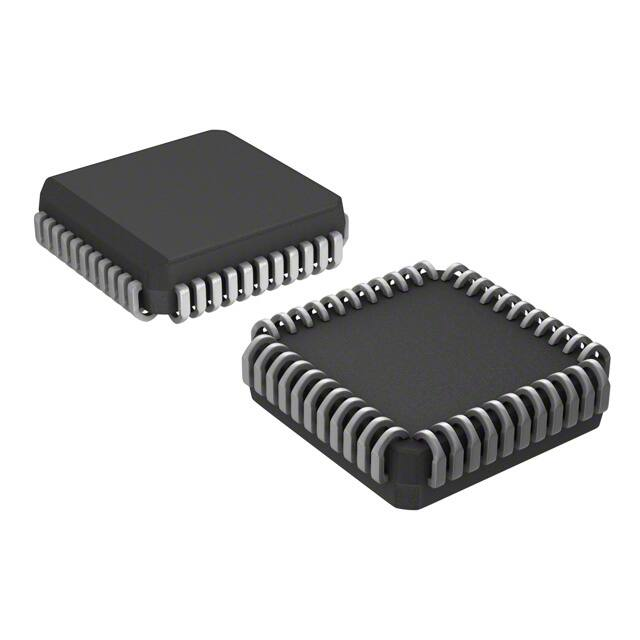
Available in 44-pin Plastic Leaded Chip Carrier (PLCC)
Operating Temperature Range -40°°C to +85°°C
FUNCTIONAL DESCRIPTION
A functional block diagram of the IDT728980 device is shown on below. The
serial ST-BUS® streams operate continuously at 2.048 Mb/s and are arranged
in 125μs wide frames each containing 32, 8-bit channels. Eight input (RX0-7)
and eight output (TX0-7) serial streams are provided in the IDT728980 device
allowing a complete 256 x 256 channel non-blocking switch matrix to be
constructed. The serial interface clock (C4i) for the device is 4.096 MHz.
The received serial data is internally converted to a parallel format by the on
chip serial-to-parallel converters and stored sequentially in a 256-position Data
Memory. By using an internal counter that is reset by the input 8 KHz frame pulse,
F0i, the incoming serial data streams can be framed and sequentially addressed.
DESCRIPTION:
The IDT728980 is a ST-BUS® compatible digital switch controlled by a
microprocessor. The IDT728980 can handle as many as 256, 64 Kbit/s input
FUNCTIONAL BLOCK DIAGRAM
C4i
F0i
VCC
Timing
Unit
RX0
TX0
Output MUX
RX1
RX2
RX3
RX4
TX1
TX2
Receive
Serial Data
Streams
Transmit
Serial Data
Streams
Data
Memory
RX5
Control Register
RX6
RX7
ODE
GND
Connection
Memory
TX3
TX4
TX5
TX6
Microprocessor Interface
TX7
5706 drw01
DS CS R/W A0/ DTA D0/
A5
D7
CCO
MARCH 2017
IDT and the IDT logo are registered trademarks of Integrated Device Technology, Inc.
1
©2017 Integrated Device Technology, Inc. All rights reserved. Product specifications subject to change without notice.
DSC-5706/2
�IDT728980 Time Slot Interchange Digital Switch
256 x 256
COMMERCIAL TEMPERATURE RANGE
TX0
TX1
TX2
DNC(1)
42
41
40
ODE
2
43
RX0
DTA
3
CCO
RX1
4
11
35
TX7
VCC
12
34
GND
F0i
13
33
D0
C4i
14
32
D1
A0
15
31
D2
A1
16
30
D3
A2
17
29
D4
DNC(1)
D5
D6
D7
CS
R/W
DS
A5
A4
A3
28
RX7
26
TX6
27
TX5
36
25
37
10
24
9
RX6
22
RX5
23
TX4
21
TX3
38
20
39
8
19
7
RX4
18
RX3
DNC(1)
NOTE:
1. DNC - Do Not Connect.
44
RX2
5
1
DNC(1)
INDEX
6
PIN CONFIGURATION
5706 drw02
PLCC: 0.05in. pitch, 0.65in. x 0.65in.
(J44, order code: J)
TOP VIEW
PIN DESCRIPTIONS
SYMBOL
GND
VCC
DTA
RX0-7
F0i
C4i
A0-A5
DS
R/W
NAME
Ground.
VCC
Data Acknowledgment
(Open Drain)
RX Input 0 to 7
Frame Pulse
Clock
Address 0 to 5
Data Strobe
I/O
O
I
I
I
I
I
Read/Write
Chip Select
Data Bus 0 to 7
I
I
I/O
O
ODE
TX Outputs 0 to 7
(Three-state Outputs)
Output Drive Enable
CCO
Control Channel Output
O
CS
D0-D7
TX0-7
I
DESCRIPTION
Ground Rail.
+5.0 Volt Power Supply.
This active LOW output indicates that a data bus transfer is complete. A pull-up resistor is required at this
output.
Serial data input streams. These streams have 32 channels at data rates of 2.048 Mb/s.
This input identifies frame synchronization signals formatted to ST-BUS® specifications.
4.096 MHz serial clock for shifting data in and out of the data streams.
These lines provide the address to IDT728980 internal registers.
This is the input for the active HIGH data strobe on the microprocessor interface. This input operates with
CS to enable the internal read and write generation.
This input controls the direction of the data bus lines (D0-D7) during a microprocessor access.
Active LOW input enabling a microprocessor read or write of control register or internal memories.
These pins provide microprocessor access to data in the internal control register. Connection Memory HIGH,
Connection Memory LOW and data memory.
Serial data output streams. These streams are composed of 32, 64 Kbit/s channels at data rates of 2.048 Mb/s.
This is an output enable for the TX0-7 serial outputs. If this input is LOW, TX0-7 are high-impedance. If this is
HIGH, each channel may still be put into high-impedance by software control.
This output is a 2.048 Mb/s line which contains 256 bits per frame. The level of each bit is controlled by the
contents of the CCO bit in the Connection Memory HIGH locations.
2
�IDT728980 Time Slot Interchange Digital Switch
256 x 256
COMMERCIAL TEMPERATURE RANGE
FUNCTIONAL DESCRIPTION (Cont'd)
device varies according to the combination of input and output streams and the
movement within the stream from channel to channel. Data received on an input
stream must first be stored in Data Memory before it is sent out.
As information enters the IDT728980 it must first pass through an internal
serial-to-parallel converter. Likewise, before data leaves the device, it must
pass through the internal parallel-to-serial converter. This data preparation has
an effect on the channel positioning in the frame immediately following the
incoming frame-mainly, data cannot leave in the same time slot, or in the time
slot immediately following. Therefore, information that is to be output in the same
channel position as the information is input, relative to the frame pulse, will be
output in the following frame. As well, information switched to the channel
immediately following the input channel will not be output in the time slot
immediately following, but in the next timeslot allocated to the output channel, one
frame later.
Whether information can be output during a following timeslot after the
information entered the IDT728980 depends on which RX stream the channel
information enters on and which TX stream the information leaves on. This is
caused by the order in which input stream information is placed into Data Memory
and the order in which stream information is queued for output. Table 1 shows
the allowable input/output stream combinations for the minimum 2 channel delay.
Data to be output on the serial streams may come from two sources: Data
Memory or Connection Memory. The Connection Memory is 16 bits wide and
is split into two 8-bit blocks—Connection Memory HIGH and Connection
Memory LOW. Each location in Connection Memory is associated with a
particular channel in the output stream so as to provide a one-to-one correspondence between the two memories. This correspondence allows for per channel
control for each TX output stream. In Processor Mode, data output on the TX
stream is taken from the Connect Memory Low and originates from the
microprocessor (Figure 2). Where as in Connection Mode (Figure 1), data is
read from Data Memory using the address in Connection Memory. Data
destined for a particular channel on the serial output stream is read during the
previous channel time slot to allow time for memory access and internal parallelto-serial conversion.
CONNECTION MODE
In Connection Mode, the addresses of input source for all output channels
are stored in the Connect Memory Low. The Connect Memory Low locations
are mapped to corresponding 8-bit x 32-channel output. The contents of the
Data Memory at the selected address are then transferred to the parallel-toserial converters. By having the output channel to specify the input channel
through the connect memory, input channels can be broadcast to several output
channels.
SOFTWARE CONTROL
If the A5 address line input is LOW then the IDT728980 Internal Control
Register is addressed. If A5 input line is high, then the remaining address input
lines are used to select the 32 possible channels per input or output stream. The
address input lines and the Stream Address bits (STA) of the Control register
give the user the capability of selecting all positions of IDT728980 Data and
Connection memories. The IDT728980 memory mapping is illustrated in
Table 2 and Figure 3.
The data in the control register (Table 3) consists of Memory Select and
Stream Address bits, Split Memory and Processor Mode bits. In Split Memory
mode (Bit 7 of the Control register) reads are from the Data Memory and writes
are to the Connect Memory as specified by the Memory Select Bits (Bits 4 and
3 of the Control Register). The Memory Select bits allow the Connect Memory
High or LOW or the Data Memory to be chosen, and the Stream Address bits
define internal memory subsections corresponding to input or output streams.
The Processor Enable bit (bit 6) places EVERY output channel on every
output stream in Processor Mode; i.e., the contents of the Connect Memory LOW
(CML, see Table 5) are output on the TX output streams once every frame
unless the ODE input pin is LOW. If PE bit is HIGH, then the IDT728980 behaves
as if bits 2 (Channel Source) and 0 (Output Enable) of every Connect Memory
High (CMH) locations were set to HIGH, regardless of the actual value. If PE
is LOW, then bit 2 and 0 of each Connect Memory High location operates
normally. In this case, if bit 2 of the CMH is HIGH, the associated TX output
channel is in Processor Mode. If bit 2 of the CMH is LOW, then the contents of
the CML define the source information (stream and channel) of the time slot that
is to be switched to an output.
PROCESSOR MODE
In Processor Mode the CPU writes data to specific Connect Memory Low
locations which are to be output on the TX streams. The contents of the Connect
Memory Low are transferred to the parallel-to-serial converter one channel
before it is to be output and are transmitted each frame to the output until it is
changed by the CPU.
CONTROL
The Connect Memory High bits (Table 4) control the per-channel functions
available in the IDT728980. Output channels are selected into specific modes
such as: Processor Mode or Connection mode and Output Drivers Enabled
or in three-state condition. There is also one bit to control the state of the CCO
output pin.
OUTPUT DRIVE ENABLE (ODE)
The ODE pin is the master output control pin. If the ODE input is held LOW
all TDM outputs will be placed in high impedance regardless Connect Memory
High programming. However, if ODE is HIGH, the contents of Connect Memory
High control the output state on a per-channel basis.
DELAY THROUGH THE IDT728980
The transfer of information from the input serial streams to the output serial
streams results in a delay through the device. The delay through the IDT728980
RX
Receive
Serial Data
Streams
Data
Memory
Connection
Memory
Transmit
Serial Data
Streams
Receive
Serial Data
Streams
TX
Data
Memory
Connection
Memory
Transmit
Serial Data
Streams
TX
5706 drw06
Microprocessor
5706 drw05
Figure 2. Processor Mode
Figure 1. Connection Mode
3
�IDT728980 Time Slot Interchange Digital Switch
256 x 256
COMMERCIAL TEMPERATURE RANGE
If the ODE input pin is LOW, then all the serial outputs are high-impedance.
If ODE is HIGH, then bit 0 (Output Enable) of the CMH location enables (if HIGH)
or disables (if LOW) the output stream and channel.
The contents of bit 1 (CCO) of each Connection Memory High Location (see
Table 4) is output on CCO pin once every frame. The CCO pin is a 2.048 Mb/s
output, which carries 256 bits. If CCO bit is set HIGH, the corresponding bit on
CCO output is transmitted HIGH. If CCO is LOW, the corresponding bit on the
CCO output is transmitted in LOW. The contents of the 256 CCO bits of the CMH
are transmitted sequentially on to the CCO output pin and are synchronous to
the TX streams. To allow for delay in any external control circuitry the contents
of the CCO bit is output one channel before the corresponding channel on the
TX streams. For example, the contents of CCO bit in position 0 (corresponding
to TX0, CH0) is transmitted synchronously with the TX channel 31, bit 7. Bit 1's
of CMH for channel 1 of stream 0-7 are output synchronously with TX channel
0 bits 7-0.
Input
Output Stream
0
1,2,3,4,5,6,7
1
2
3
4
5
6
7
3,4,5,6,7
5,6,7
7
1,2,3,4,5,6,7
3,4,5,6,7
5,6,7
7
INITIALIZATION OF THE IDT728980
On initialization or power up, the contents of the Connection Memory High
can be in any state. This is a potentially hazardous condition when multiple TX
outputs are tied together to form matrices. The ODE pin should be held low on
power up to keep all outputs in the high impedance condition until the contents
of the CMH are programmed.
During the microprocessor initialization routine, the microprocessor should
program the desired active paths through the matrices, and put all other channels
into the high impedance state. Care should be taken that no two connected TX
outputs drive the bus simultaneously. With the CMH setup, the microprocessor
controlling the matrices can bring the ODE signal high to relinquish high
impedance state control to the Connection Memory High bits outputs.
A5 A4 A3 A2 A1 A0
LOCATION
0
1
1
X
0
0
X
0
0
X
0
0
X
0
0
X
0
1
00-1F
20
21
Control Register(1)
Channel 0(2)
Channel 1(2)
•
•
•
•
•
•
•
•
•
•
•
•
•
•
•
•
•
•
•
•
•
•
•
•
1
1
1
1
1
1
3F
Channel 31(2)
NOTES:
1. Writing to the Control Register is the only fast transaction.
2. Memory and stream are specified by the contents of the Control Register.
Table 1. Input Stream to Output Stream Combinations that can Provide the
Minimum 2-Channel Delay
Control Register
HEX ADDRESS
CRb7
CRb6
The Control Register is only accessed when A5=0.
All other address bits have no effect when A5=0.
When A5 =1, only 32 bytes are randomly accessable via
A0-A4 at any one instant. Which 32 bytes are
accessed is determined by the state of CRb0 -CRb4.
The 32 bytes correlate to 32 channel of one ST-BUS®
stream.
Table 2. Address Mapping
CRb5
CRb4
0
1
1
CRb4
CRb3
CRb2
CRb1
CRb0
CRb3
1
0
1
Connection Memory High
Connection Memory Low
Data Memory
Channel 0
Channel 0
Channel 0
Channel 0
Channel 0
Channel 0
Channel 0
Channel 0
Channel 1
Channel 1
Channel 1
Channel 1
Channel 1
Channel 1
Channel 1
Channel 1
100000
100001
Channel 2
Channel 2
Channel 2
Channel 2
Channel 2
Channel 2
Channel 2
Channel 2
100010
Channel 31
Channel 31
Channel 31
Channel 31
Channel 31
Channel 31
Channel 31
Channel 31
CRb2
0
0
0
0
1
1
1
1
CRb1
0
0
1
1
0
0
1
1
111111
External Address Bits
CRb0 Stream
0
0
1
1
2
0
1
3
0
4
1
5
0
6
1
7
A5-A0
5706 drw07
Figure 3. Address Mapping
4
�IDT728980 Time Slot Interchange Digital Switch
256 x 256
COMMERCIAL TEMPERATURE RANGE
Mode Control
Bits
7
Bit
6
(unused)
Memory Select
Bits
5
4
Name
3
Stream Address Bits
2
1
0
Description
7
SM (Split Memory)
When 1, all subsequent reads are from the Data Memory and writes are to the Connection Memory LOW, except
when the Control Register is accessed again. When 0, the Memory Select bits specify the memory for the
operations. In either case, the Stream Address Bits select the subsection of the memory which is made available.
6
PE (Processor Mode)
When 1, the contents of the Connection Memory LOW are output on the Serial Output streams except when the ODE
pin is LOW. When 0, the Connection Memory bits for each channel determine what is output.
5
unused
4-3
MS1-MS0
(Memory Select Bits)
0-0 - Not to be used.
0-1 - Data Memory (read only from the microprocessor port)
1-0 - Connection Memory LOW
1-1 - Connection Memory is HIGH
2-0
STA2-0
(Stream Address Bits)
The number expressed in binary notation on these bits refers to the input or output stream which corresponds to the
subsection of memory made accessible for subsequent operations.
Table 3. Control Register Configuration
No Corresponding Memory
- These bits give 0s if read
7
Bit
6
5
4
Name
Per Channel Control Bits
3
2
1
0
Description
2
CS (Channel Source)
When 1, the contents of the corresponding location in Connection Memory LOW are output on the location's channel
and stream. When 0, the contents of the corresponding location in Connection Memory LOW act as an address for the
Data Memory and determine the source of the connection to the location's channel and stream.
1
CCO (CCO Bit)
This bit is output on the CCO pin one channel early. The CCO bit for stream 0 is output first.
0
OE (Output Enable)
If the ODE pin is HIGH and bit 6 of the Control Register is 0, then this bit enables the output drive for the location's
channel and stream. This allows individuals channels on individuals streams to be made high-impedance, allowing
switching matrices to be constructed. A 1 enables the driver and a 0 disables it.
Table 4. Connection Memory High Register
Stream Address Bits
7
Bit
7-5(1)
6
Channel Address Bits
5
4
Name
Stream Address Bits
4-0(1) Channel Address Bits
3
2
1
0
Description
The number expressed in binary notation on these 3 bits are the number of the stream for the source of the connection.
Bit 7 is the most significant bit, e.g., If bit 7 is 1, bit 6 is 0 and bit 5 is 0 then the source of the connection is a channel on
RX4.
The number expressed in binary notation on these 5 bits is the number of the channel which is the source of the
connection (the stream where the channel lies is defined by bits 7, 6 and 5). Bit 4 is the most significant bit, e.g., if bit 4
is 1, bit 3 is 0, bit 2 is 0, bit 1 is 1 and bit 0 is 1, then the source of the connection is channel 19.
NOTE:
1. If bit 2 of the corresponding Connection HIGH location is 1 or bit 6 of the Control Register is 1, then these entire 8 bits are output on the channel and stream associated with
this location. Otherwise, the bits are used as indicated to define the source of the connection which is output on the channel and stream associated with this location.
Table 5. Connection Memory Low Register
5
�IDT728980 Time Slot Interchange Digital Switch
256 x 256
COMMERCIAL TEMPERATURE RANGE
ABSOLUTE MAXIMUM RATINGS
Symbol
Parameter
Min.
Max.
Unit
VCC - GND
-0.3
7
V
Vi
Voltage on Digital Inputs
GND - 0.3
VCC +0.3
V
VO
Voltage on Digital Outputs
GND - 0.3
VCC +0.3
V
IO
Current at Digital Outputs
40
mA
TS
Storage Temperature
+150
°C
PD
Package Power Dissapation
2
W
-65
RECOMMENDED OPERATING
CONDITIONS
(1)
Symbol
Parameter
Typ.(1)
Max.
Unit
4.75
⎯
5.25
V
0
⎯
VCC
V
-40
⎯
+85
°C
Min.
VCC
Positive Supply
VI
Input Voltage
TOP
Operating Temperature
Commercial
NOTE:
1. Typical figures are at 25°C and are for design aid only; not guaranteed and not subject
to production testing.
NOTE:
1. Exceeding these values may cause permanent damage. Functional operation
under these conditions is not implied.
DC ELECTRICAL CHARACTERISTICS
Symbol
Parameter
Min.
Typ.(1)
Max.
Units
Test Conditions
10
mA
Outputs Unloaded
ICC
Supply Current
⎯
7
VIH
Input High Voltage
2.0
⎯
⎯
V
VIL
Input Low Voltage
⎯
⎯
0.8
V
IIL
Input Leakage
⎯
⎯
5
μA
CI
Input Capacitance
⎯
8
⎯
pF
VOH
Output High Voltage
2.4
⎯
⎯
V
IOH = 10mA
VI between GND and VCC
IOH
Output High Current
10
15
⎯
mA
Sourcing. VOH = 2.4V
VOL
Output Low Voltage
⎯
⎯
0.4
V
IOL = 5mA
IOL
Output Low Current
5
10
⎯
mA
Sinking. VOL = 0.4V
IOZ
High Impedance Leakage
⎯
⎯
5
μA
VO between GND and VCC
CO
Output Pin Capacitance
⎯
8
⎯
pF
NOTE:
1. Typical figures are at 25°C and are for design aid only; not guaranteed and not subject to production testing.
Test Point
VCC
S1 is open circuit except when testing output
levels or high impedance states.
S2
S2 is switched to VCC or GND when testing
output levels or high impedance states.
RL
Output
Pin
S1
CL
GND
GND
5706 drw08
Figure 4. Output Load
6
�IDT728980 Time Slot Interchange Digital Switch
256 x 256
COMMERCIAL TEMPERATURE RANGE
AC ELECTRICAL CHARACTERISTICS
(1)
⎯ CLOCK TIMING
Typ.(2)
Symbol
Characteristics
Min.
tCLK
Clock Period(3)
Max.
Unit
220
244
300
ns
tCH
Clock Width High
95
122
150
ns
tCL
Clock Width Low
110
122
150
ns
tCTT
Clock Transition Time
⎯
20
⎯
ns
tFPS
Frame Pulse Setup Time
20
⎯
200
ns
tFPH
Frame Pulse Hold Time
0.020
⎯
50
μs
tFPW
Frame Pulse Width
⎯
244
⎯
ns
NOTE:
1. Timing is over recommended temperature and power supply voltages.
2. Typical figures are at 25°C and are for design aid only; not guaranteed and not subject to production testing.
3. Contents of Connection Memory are not lost if the clock stops, however, TX outputs go into the high impedance state.
C4i
F0i
Channel 31
Bit 0
Bit Cells
Channel 0
Bit 7
5706 drw09
Figure 5. Frame Alignment
tCLK
tCTT
tCTT
tCHL
tCL
t CH
C4i
((
))
tFPH
tFPS
tFPH
tFPS
tFPW
F0i
5706 drw10
Figure 6. Clock Timing
7
�IDT728980 Time Slot Interchange Digital Switch
256 x 256
COMMERCIAL TEMPERATURE RANGE
AC ELECTRICAL CHARACTERISTICS
Symbol
Characteristics
(1)
⎯ SERIAL STREAM TIMING
Min.
Typ.(2)
Max.
Unit
Test Conditions
tTAZ
TX0-7 Delay - Active to High Z
20
30
60
ns
RL = 1KΩ(3), CL = 150pF
tTZA
TX0-7 Delay - High Z to Active
25
45
70
ns
CL = 150pF
tTAA
TX0-7 Delay - Active to Active
30
45
70
ns
CL = 150pF
tTOH
TX0-7 Hold Time
25
45
⎯
ns
CL = 150pF
tOED
Output Driver Enable Delay
⎯
40
70
ns
RL = 1KΩ(3), CL = 150pF
tXCH
External Control Hold Time
0
10
⎯
ns
CL = 150pF
tXCD
External Control Delay
⎯
20
40
ns
CL = 150pF
tSIS
Serial Input Setup Time
⎯
-40
-20
ns
tSIH
Serial Input Hold Time
90
⎯
⎯
ns
NOTE:
1. Timing is over recommended temperature and power supply voltages.
2. Typical figures are at 25°C and are for design aid only; not guaranteed and not subject to production testing.
3. High Impedance is measured by pulling to the appropriate rail with RL, with timing corrected to cancel time taken to discharge CL.
Bit Cell Boundary
ODE
C4i
tOED
tOED
tTAZ
tTOH
TX0-7
5706 drw12
TX0-7
Figure 8. Output Driver Enable
tTZA
TX0-7
tTAA
tTOH
Bit Cell Boundaries
TX0-7
C4i
t XCD
t XCH
tSIS
CCO
tSIH
RX0-7
5706 drw11
5706 drw13
Figure 7. Serial Outputs and External Control
Figure 9. Serial Inputs
8
�IDT728980 Time Slot Interchange Digital Switch
256 x 256
COMMERCIAL TEMPERATURE RANGE
AC ELECTRICAL CHARACTERISTICS
Symbol
Characteristics
(1)
⎯ PROCESSOR BUS
Min.
Typ.(2)
Max.
Unit
tCSS
Chip Select Setup Time
10
0
⎯
ns
Test Conditions
tRWS
Read/Write Setup Time
10
⎯
⎯
ns
tADS
Address Setup Time
10
⎯
⎯
ns
tAKD
Acknowledgment Delay Fast
⎯
30
60
ns
CL = 150pF
tAKD
Acknowledgment Delay Slow
2.7
⎯
7.2
cycles
C4i cycles(4)
tFWS
Fast Write Data Setup Time
20
⎯
⎯
ns
tSWD
Slow Write Data Delay
⎯
2.0
1.7
cycles
C4i cycles
tRDS
Read Data Setup Time
⎯
⎯
0.5
cycles
C4i cycles, CL = 150pF
tDHT
Data Hold Time Read
20
⎯
⎯
ns
RL = 1KΩ(3), CL = 150pF
tDHT
Data Hold Time Write
20
10
⎯
ns
tRDZ
Read Data to High Impedance
⎯
30
60
ns
tCSH
Chip Select Hold Time
0
⎯
⎯
ns
tRWH
Read/Write Hold Time
0
⎯
⎯
ns
tADH
Address Hold Time
0
⎯
⎯
ns
tAKH
Acknowledgment Hold Time
10
20
40
ns
RL = 1KΩ(3), CL = 150pF
RL = 1KΩ(3), CL = 150pF
NOTE:
1. Timing is over recommended temperature and power supply voltages.
2. Typical figures are at 25°C and are for design aid only; not guaranteed and not subject to production testing.
3. High Impedance is measured by pulling to the appropriate rail with RL, with timing corrected to cancel time taken to discharge CL.
4. Processor accesses are dependent on the C4i clock, and so some things are expressed as multiples of the C4i.
DS
tCSS
t CSH
tRWS
tRWH
tADS
t ADH
CS
R/W
A5-A0
tAKD
tAKH
DTA
t RDS
tSWD
tRDZ
tFWS
tDHT
D7-D0
5706 drw14
Figure 10. Processor Bus
9
�ORDERING INFORMATION
XXXXXX
Device Type
XX
Package
X
X
Process/
Temperature
Range
X
Blank
8
Tube
Tape and Reel
BLANK
Commercial (-40°C to +85°C)
G
Green
J
Plastic Leaded Chip Carrier (PLCC, J44)
728980
256 x 256 ⎯ Time Slot Interchange Digital Switch
5610 drw25
DATASHEET DOCUMENT HISTORY
05/23/2000
08/18/2000
01/24/2001
03/13/2017
pgs.
pgs.
pgs.
pgs.
1, 2, and 10.
1, 2, and 10.
1 and 6.
1, 2, and 10.
CORPORATE HEADQUARTERS
6024 Silver Creek Valley Road
San Jose, CA 95138
for SALES:
800-345-7015 or 408-284-8200
fax: 408-284-2775
www.idt.com
10
for Tech Support:
408-360-1753
email: FIFOhelp@idt.com
�IMPORTANT NOTICE AND DISCLAIMER
RENESAS ELECTRONICS CORPORATION AND ITS SUBSIDIARIES (“RENESAS”) PROVIDES TECHNICAL
SPECIFICATIONS AND RELIABILITY DATA (INCLUDING DATASHEETS), DESIGN RESOURCES (INCLUDING
REFERENCE DESIGNS), APPLICATION OR OTHER DESIGN ADVICE, WEB TOOLS, SAFETY INFORMATION, AND
OTHER RESOURCES “AS IS” AND WITH ALL FAULTS, AND DISCLAIMS ALL WARRANTIES, EXPRESS OR IMPLIED,
INCLUDING, WITHOUT LIMITATION, ANY IMPLIED WARRANTIES OF MERCHANTABILITY, FITNESS FOR A
PARTICULAR PURPOSE, OR NON-INFRINGEMENT OF THIRD PARTY INTELLECTUAL PROPERTY RIGHTS.
These resources are intended for developers skilled in the art designing with Renesas products. You are solely responsible
for (1) selecting the appropriate products for your application, (2) designing, validating, and testing your application, and (3)
ensuring your application meets applicable standards, and any other safety, security, or other requirements. These
resources are subject to change without notice. Renesas grants you permission to use these resources only for
development of an application that uses Renesas products. Other reproduction or use of these resources is strictly
prohibited. No license is granted to any other Renesas intellectual property or to any third party intellectual property.
Renesas disclaims responsibility for, and you will fully indemnify Renesas and its representatives against, any claims,
damages, costs, losses, or liabilities arising out of your use of these resources. Renesas' products are provided only subject
to Renesas' Terms and Conditions of Sale or other applicable terms agreed to in writing. No use of any Renesas resources
expands or otherwise alters any applicable warranties or warranty disclaimers for these products.
(Rev.1.0 Mar 2020)
Corporate Headquarters
Contact Information
TOYOSU FORESIA, 3-2-24 Toyosu,
Koto-ku, Tokyo 135-0061, Japan
www.renesas.com
For further information on a product, technology, the most
up-to-date version of a document, or your nearest sales
office, please visit:
www.renesas.com/contact/
Trademarks
Renesas and the Renesas logo are trademarks of Renesas
Electronics Corporation. All trademarks and registered
trademarks are the property of their respective owners.
© 2020 Renesas Electronics Corporation. All rights reserved.
�


 工商网监
湘ICP备2023018690号
工商网监
湘ICP备2023018690号
