3.3 VOLT TIME SLOT INTERCHANGE
DIGITAL SWITCH WITH RATE
MATCHING 16,384 X 16,384 CHANNELS
FEATURES:
•
•
•
•
•
•
•
•
•
•
•
•
•
•
•
•
Up to 64 serial input and output streams
Maximum 16,384 x 16,384 channel non-blocking switching
Accepts data streams at 2.048Mb/s, 4.096Mb/s, 8.192Mb/s,
16.384Mb/s or 32.768Mb/s
Rate matching capability: rate selectable on both RX and TX
in eight groups of 8 streams
Optional Output Enable Indication Pins for external driver
High-Z control
Per-channel Variable Delay Mode for low-latency applications
Per-channel Constant Delay Mode for frame integrity applications
Enhanced Block programming capabilities
TX/RX Internal Bypass
Automatic identification of ST-BUS and GCI serial streams
Per-stream frame delay offset programming
Per-channel High-Impedance output control
Per-channel processor mode to allow microprocessor writes to TX
streams
Bit Error Rate Testing (BERT) for testing
Direct microprocessor access to all internal memories
•
•
•
IDT72V73263
Selectable Synchronous and Asynchronous Microprocessor
bus timing modes
IEEE-1149.1 (JTAG) Test Port
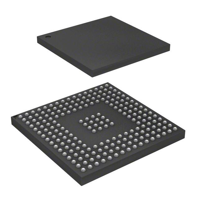
Available in 208-pin (17mm x 17mm) Plastic Ball Grid Array (PBGA)
Operating Temperature Range -40°°C to +85°°C
DESCRIPTION:
The IDT72V73263 has a non-blocking switch capacity of 16,384 x 16,384
channels at 32.768Mb/s. With 64 inputs and 64 outputs, programmable per
stream control, and a variety of operating modes the IDT72V73263 is
designed for the TDM time slot interchange function in either voice or data
applications.
Some of the main features of the IDT72V73263 are LOW power 3.3 Volt
operation, automatic ST-BUS® /GCI sensing, memory block programming,
simple microprocessor interface , JTAG Test Access Port (TAP) and per
stream programmable input offset delay, variable or constant throughput
modes, output enable and processor mode, BER testing, bypass mode, and
advanced block programming.
FUNCTIONAL BLOCK DIAGRAM
IDT and the IDT logo are registered trademarks of Integrated Device Technology, Inc. The ST-BUS is a trademark of Mitel Corp.
September 2007
1
2003 Integrated Device Technology, Inc. All rights reserved. Product specifications subject to change without notice
DSC-6160/4
�IDT72V73263 3.3V TIME SLOT INTERCHANGE
DIGITAL SWITCH WITH RATE MATCHING 16,384 x 16,384 CHANNELS
INDUSTRIAL TEMPERATURE RANGE
PIN CONFIGURATIONS
A1 BALL PAD CORNER
A
C32i
R ESET
ODE
RX1
RX4
TX0
TX4
TX7
TX12/
OEI4
TX15/
OEI7
RX11
RX15
RX20
TX16
TX18
TX19
F32i
Vcc
RX0
RX2
RX5
TX1
TX5
TX8/
OEI0
TX11/
OEI3
TX14/
OEI6
RX10
RX14
RX19
RX23
TX17
TX20
S/A (1)
TMS
TDI
RX3
RX6
TX2
TX6
TX9/
OEI1
TX10/
OEI2
TX13/
OEI5
RX9
RX13
RX18
RX22
TX22
TX21
TDO
TCK
TR ST
DS
RX7
TX3
VCC
VCC
VCC
VCC
RX8
RX12
RX17
RX21
TX24/
OEI16
TX23
CS
R/W
A0
A1
RX16
TX27/
OEI19
TX26/
OEI18
TX25/
OEI17
A2
A3
A4
A5
TX31/
OEI23
TX30/
OEI22
TX29/
OEI21
TX28/
OEI20
A6
A7
A8
VCC
GND
GND
GND
GND
VCC
RX26
RX25
RX24
A9
A10
A11
VCC
GND
GND
GND
GND
VCC
RX29
RX28
RX27
A14
A13
A12
VCC
GND
GND
GND
GND
VCC
RX30
RX31
RX32
D15
D TA/
BEH
A15
VCC
GND
GND
GND
GND
VCC
RX33
RX34
RX35
D12
D13
D14
BEL
RX36
RX37
RX38
RX39
D8
D9
D10
D11
TX32
TX33
TX34
TX35
D5
D6
D7
RX56
TX60/
OEI52
TX56/
OEI48
VCC
VCC
VCC
VCC
RX51
RX47
TX36
TX37
TX38
TX39
D3
D4
RX60
RX57
TX61/
OEI53
TX57/
OEI49
TX53
TX50
TX49
RX54
RX50
RX46
RX43
TX40/
OEI32
TX41/
OE33
TX42/
OEI34
D2
RX63
RX61
RX58
TX62/
OEI54
TX58/
OEI50
TX54
TX51
TX48
RX53
RX49
RX45
RX42
RX40
TX46/
OEI38
TX43/
OEI35
D1
D0
RX62
RX59
TX63/
OEI55
TX59/
OEI51
TX55
TX52
RX55
RX52
RX48
RX44
RX41
TX47/
OEI39
TX45/
OEI37
TX44/
OEI36
1
2
3
4
5
6
7
8
9
10
11
12
13
14
15
B
C
D
E
F
G
H
J
K
L
M
N
P
R
T
16
6160 drw03
NOTE:
1. S/A should be tied directly to VCC or GND for proper
operation.
PBGA: 1mm pitch, 17mm x 17mm (BB208-1 order code: BB)
TOP VIEW
2
�IDT72V73263 3.3V TIME SLOT INTERCHANGE
DIGITAL SWITCH WITH RATE MATCHING 16,384 x 16,384 CHANNELS
INDUSTRIAL TEMPERATURE RANGE
PIN DESCRIPTION
SYMBOL
NAME
A0-A15
Address 0-15
BEL
I/O
PBGA
PIN NO.
DESCRIPTION
I
*See PBGA
Table Below
These address lines access all internal memories.
Byte Enable LOW
I
L4
In synchronous mode, this input will enable the lower byte (D0-7) on to the data bus.
C32i
Clock
I
A1
Serial clock for shifting data in/out on the serial data streams. This input accepts a
32.768MHz clock.
CS
Chip Select
I
E1
Active LOW input used by a microprocessor to activate the microprocessor port of the
device.
D0-15
Data Bus 0-15
I/O
*See PBGA
Table Below
DS
Data Strobe
I
D4
DTA/BEH
F32i
Data Transfer
Acknowledgment
Active LOW Output
Frame Pulse
I/O
K2
I
GND
B1
*See PBGA
Table Below
These pins are the data bus of the microprocessor port.
This active LOW input works in conjunction with CS to enable the read and write
operations. This active LOW input sets the data bus lines (D0-D15).
In asynchronous mode this pin indicates that a data bus transfer is complete. When the
bus cycle ends,this pin drives HIGH and then High-Z allowing for faster bus cycles
with a weaker pull-up resistor. A pull-up resistor is required to hold a HIGH level
when the pin is High-Z. When the device is in /Byte Enable HIGH synchronous
bus mode, this pin acts as an input and will enable the upper byte (D8-15) on to the
data bus.
This input accepts and automatically identifies frame synchronization signals formatted
according to ST-BUS and GCI specifications.
Ground.
ODE
Output Drive Enable
I
A3
This is the output enable control for the TX serial outputs. When ODE input is LOW and
the OSB bit of the CR register is LOW, all TX outputs are in a High-Impedance state. If
this input is HIGH, the TX output drivers are enabled. However, each channel may
still be put into a High-Impedance state by using the per channel control bits in the
Connection Memory HIGH.
RX0-63
RX Input 0 to 63
I
*See PBGA
Table Below
RESET
Device Reset:
I
A2
This input (active LOW) puts the device in its reset state that clears the device internal
counters, registers and brings TX0-63 and microport data outputs to a High-Impedance
state. The RESET pin must be held LOW for a minimum of 20ns to reset the device.
R/W
Read/Write
I
E2
This input controls the direction of the data bus lines (D0-D15) during a microprocessor
access.
S/A
Synchronous/
Asynchronous
Bus Mode
I
C1
This input will select between asynchronous microprocessor bus timing and synchronous
microprocessor bus timing. In synchronous mode, DTA/BEH acts as the BEH input and is
used in conjunction with BEL to output data on the data bus. In asynchronous bus mode,
BEL is tied LOW and DTA/BEH acts as the DTA, data bus acknowledgment output.
TCK
Test Clock
I
D2
Provides the clock to the JTAG test logic.
TDI
Test Serial Data In
I
C3
JTAG serial test instructions and data are shifted in on this pin. This pin is pulled HIGH
by an internal pull-up when not driven.
TDO
Test Serial Data Out
O
D1
JTAG serial data is output on this pin on the falling edge of TCK. This pin is held in
High-Impedance state when JTAG scan is not enabled.
TMS
Test Mode Select
I
C2
JTAG signal that controls the state transitions of the TAP controller. This pin is pulled
HIGH by an internal pull-up when not driven.
TRST
Test Reset
I
D3
Asynchronously initializes the JTAG TAP controller by putting it in the Test-LogicReset state. This pin is pulled by an internal pull-up when not driven. This pin should
be pulsed LOW on power-up, or held LOW, to ensure that the device is in the normal
functional mode.
Serial data Input Stream. These streams may have data rates of 2.048Mb/s,
4.096Mb/s, 8.192Mb/s, 16.384Mb/s, or 32.768Mb/s depending upon the selection in Receive
Data Rate Selection Register (RDRSR).
3
�IDT72V73263 3.3V TIME SLOT INTERCHANGE
DIGITAL SWITCH WITH RATE MATCHING 16,384 x 16,384 CHANNELS
INDUSTRIAL TEMPERATURE RANGE
PIN DESCRIPTION (CONTINUED)
SYMBOL
NAME
I/O
PBGA
PIN NO.
TX0-7
TX16-23
TX32-39
TX48-55
TX Output
O
*See PBGA
Table Below
Serial data Output Stream. These streams may have data rates of 2.048Mb/s,
4.096Mb/s, 8.192Mb/s,16.384Mb/s, or 32.768Mb/s depending upon the selection in
Transmit Data Rate Selection Register (TDRSR). If G0/G2/G4/G6 are programmed to
32.768Mb/s mode the corresponding odd group is unavailable (G1/G3/G5G7).
O
*See PBGA
Table Below
When output streams are selected via TDRSR, these pins are the TX output streams.
When output enable indication function is selected, these pins reflect the active or HighImpedance status for the corresponding TX output stream.
*See PBGA
Table Below
+3.3 Volt Power Supply.
TX8-15/OEI0-7
TX Output /Output
TX24-31/OEI16-23 Enable Indication
TX40-47/OEI32-39
TX56-63/OEI48-55
VCC
DESCRIPTION
PBGA PIN NUMBER TABLE
SYMBOL
NAME
I/O
A0-A15
Address A0-15
I
E3, E4, F1, F2, F3, F4, G1, G2, G3, H1, H2, H3, J3, J2, J1, K3.
D0-D15
Data Bus 0-15
I/O
T2, T1, R1, P1, P2, N1, N2, N3, M1, M2, M3, M4, L1, L2, L3, K1.
GND
Ground
RX0-63
RX Input 0 to 63
I
B3, A4, B4, C4, A5, B5, C5, D5, D11, C11, B11, A11, D12, C12, B12, A12, E13, D13, C13, B13, A13, D14, C14 , B14,
G16, G15, G14, H16, H15, H14, J14, J15, J16, K14, K15, K16, L13, L14, L15, L16, R14, T13, R13, P13, T12, R12, P12,
N12, T11, R11, P11, N11, T10, R10, P10, T9, N4, P4, R4, T4, P3, R3, T3, R2.
TX0-TX7
TX16-23
TX32-39
TX48-55
TX Output
O
A6, B6, C6, D6, A7, B7, C7, A8
A14, B15, A15, A16, B16, C16, C15, D16
M13, M14, M15, M16, N13, N14, N15, N16
R9, P9, P8, R8. T8, P7, R7, T7
O
B8, C8, C9, B9, A9, C10, B10, A10.
D15, E16, E15, E14, F16, F15, F14, F13.
P14, P15, P16, R16, T16, T15, R15, T14.
N6, P6, R6, T6, N5, P5, R5, T5.
TX8-15/OEI0-7
TX Output/Output
TX24-31/OEI16-23
TX40-47/OEI32-39
TX56-63/OEI48-55
Vcc
PIN NUMBER
G7, G8, G9, G10, H7, H8, H9, H10, J7, J8, J9, J10,K7, K8, K9, K10,
B2, D7, D8, D9, D10, G4, G13, H4, H13, J4, J13, K4, K13, N7, N8, N9, N10.
4
�IDT72V73263 3.3V TIME SLOT INTERCHANGE
DIGITAL SWITCH WITH RATE MATCHING 16,384 x 16,384 CHANNELS
DESCRIPTION (CONTINUED):
INDUSTRIAL TEMPERATURE RANGE
MOD2-0 bits are set to 0-0-1 accordingly, that particular channel will be in
Constant Delay Mode. Finally, if the MOD2-0 bits are set to 0-0-0, that particular
channel will be in Variable Delay Mode.
The IDT72V73263 is capable of switching up to 16,384 x 16,384 channels
without blocking. Designed to switch 64 Kbit/s PCM or N x 64 Kbit/s data, the
device maintains frame integrity in data applications and minimizes throughput
delay for voice applications on a per-channel basis.
The 64 serial input streams (RX) of the IDT72V73263 can be run at
2.048Mb/s, 4.096Mb/s, 8.192Mb/s, 16.384Mb/s or 32.768Mb/s allowing 32,
64, 128, 256 or 512 channels per 125µs frame. The data rates on the output
streams can independently be programmed to run at any of these data rates.
With two main operating modes, Processor Mode and Connection Mode, the
IDT72V73263 can easily switch data from incoming serial streams (Data
Memory) or from the controlling microprocessor via Connection Memory.
As control and status information is critical in data transmission, the Processor
Mode is especially useful when there are multiple devices sharing the input and
output streams.
With data coming from multiple sources and through different paths, data
entering the device is often delayed. To handle this problem, the IDT72V73263
has a Frame Offset feature to allow individual streams to be offset from the frame
pulse in half clock-cycle intervals up to +7.5 clock cycles.
The IDT72V73263 also provides a JTAG test access port, memory block
programming, Group Block Programming, RX/TX internal bypass, a simple
microprocessor interface and automatic ST-BUS /GCI sensing to shorten
setup time, aid in debugging and ease use of the device without sacrificing
capabilities.
SERIAL DATA INTERFACE TIMING
The master clock frequency of the IDT72V73263 is 32.768MHz, C32i. For
32.768Mb/s data rates, this results in a single-bit per clock. For 16.384Mb/s,
8.192Mb/s, 4.096Mb/s, and 2.048Mb/s this will result in two, four, eight, and
sixteen clocks per bit, respectively. The IDT72V73263 provides two different
interface timing modes, ST-BUS or GCI. The IDT72V73263 automatically
detects the polarity of an input frame pulse and identifies it as either ST-BUS
or GCI.
For 32.768Mb/s, in ST-BUS Mode, data is clocked out on a falling edge and
is clocked in on the subsequent rising-edge. For 16.384Mb/s, 8.192Mb/s,
4.096Mb/s, and 2.048Mb/s however there is not the typical associated clock
since the IDT72V73263 accepts only a 32.768MHz clock. As a result there will
be 2, 4, 8, and 16 clock between the 32.768Mb/s transmit edge and the
subsequently transmit edges. Although in this is the case, the IDT72V73263
will appropriately transmit and sample on the proper edge as if the respective
clock were present. See ST-BUS Timing for detail.
For 32.768Mb/s, in GCI Mode, data is clocked out on a rising edge and is
clocked in on the subsequent falling-edge. For 16.384Mb/s, 8.192Mb/s,
4.096Mb/s, and 2.048Mb/s however, again there is not the typical associated
clock since the IDT72V73263 accepts only a 32.768MHz clock. As a result there
will 2, 4, 8, and 16 clocks between the 32.768Mb/s transmit edge and the other
transmit edges. Although this is the case, the IDT72V73263 will appropriately
transmit and sample on the proper edge as if the respective clock were present.
See GCI Bus Timing for detail.
FUNCTIONAL DESCRIPTION
DATA AND CONNECTION MEMORY
All data that comes in through the RX inputs go through a serial-to-parallel
conversion before being stored into internal Data Memory. The 8 KHz frame
pulse (F32i) is used to mark the 125µs frame boundaries and to sequentially
address the input channels in Data Memory.
Data output on the TX streams may come from either the serial input streams
(Data Memory) or from the Connection Memory via the microprocessor or in
the case that RX input data is to be output, the addresses in Connection Memory
are used to specify a stream and channel of the input. The Connection Memory
is setup in such a way that each location corresponds to an output channel for
each particular stream. In that way, more than one channel can output the same
data. In Processor Mode, the microprocessor writes data to the Connection
Memory locations corresponding to the stream and channel that is to be output.
The lower half (8 least significant bits) of the Connection Memory LOW is output
every frame until the microprocessor changes the data or mode of the channels.
By using this Processor Mode capability, the microprocessor can access input
and output time-slots on a per-channel basis.
The three least significant bits of the Connection Memory HIGH are used to
control per-channel mode of the output streams. The MOD2-0 bits are used to
select Processor Mode, Constant or Variable Delay Mode, Bit Error Rate, and
the High-Impedance state of output drivers. If the MOD2-0 bits are set to 1-1-1
accordingly, only that particular output channel (8 bits) will be in the HighImpedance state. If the MOD2-0 bits are set to 1-0-0 accordingly, that particular
channel will be in Processor Mode. If the MOD2-0 bits are set to 1-0-1 a Bit Error
Rate Test pattern will be transmitted for that time slot. See BERT section. If the
DELAY THROUGH THE IDT72V73263
The switching of information from the input serial streams to the output serial
streams results in a throughput delay. The device can be programmed to
perform time-slot interchange functions with different throughput delay capabilities
on a per-channel basis. For voice applications, variable throughput delay is best
as it ensure minimum delay between input and output data. In wideband data
applications, constant throughput delay is best as the frame integrity of the
information is maintained through the switch.
The delay through the device varies according to the type of throughput delay
selected in the MOD bits of the Connection Memory.
VARIABLE DELAY MODE (MOD2-0 = 0-0-0)
In this mode, mostly for voice applications where minimum throughput delay
is desired, delay is dependent on the combination of source and destination
channels. The minimum delay achievable is a 3 channel periods of the slower
data rate.
CONSTANT DELAY MODE (MOD2-0 = 0-0-1)
In this mode, frame integrity is maintained in all switching configurations by
making use of a multiple data memory buffer. Input channel data is written into
the data memory buffers during frame n will be read out during frame n+2. In
the IDT72V73263, the minimum throughput delay achievable in Constant Delay
mode will be one frame plus one channel. See Table 14.
5
�IDT72V73263 3.3V TIME SLOT INTERCHANGE
DIGITAL SWITCH WITH RATE MATCHING 16,384 x 16,384 CHANNELS
MICROPROCESSOR INTERFACE
The IDT72V73263’s microprocessor interface looks like a standard RAM
interface to improve integration into a system. With a 16-bit address bus and
a 16-bit data bus all memories can be accessed. Using the TSI microprocessor
interface, reads and writes are mapped into Data and Connection memories.
By allowing the internal memories to be randomly accessed, the controlling
microprocessor has more time to manage other peripheral devices
and can more easily and quickly gather information and setup the switch paths.
Table 1 shows the mapping of the addresses into internal memory blocks. In
order to minimize the amount of memory mapped space however, the Memory
Select (MS1-0) bits in the Control Register must be written to first to select between
the Connection Memory HIGH, the Connection Memory LOW, or Data Memory.
Effectively, the Memory Select bits act as an internal mux to select between the
Data Memory, Connection Memory HIGH, and Connection Memory LOW.
INDUSTRIAL TEMPERATURE RANGE
internal memories. The only write operation allowed during a Software Reset
is to the Software Reset bit in the Control Register to complete the Software Reset.
CONNECTION MEMORY CONTROL
If the ODE pin and the Output Standby bit are LOW, all output channels will
be in three-state. See Table 2 for detail.
If MOD2-0 of the Connection Memory HIGH is 1-0-0 accordingly, the output
channel will be in Processor Mode. In this case the lower eight bits of the
Connection Memory LOW are output each frame until the MOD2-0 bits are
changed. If MOD2-0 of the Connection Memory HIGH are 0-0-1 accordingly,
the channel will be in Constant Delay Mode and bits 14-0 are used to address
a location in Data Memory. If MOD2-0 of the Connection Memory HIGH are
0-0-0, the channel will be in Variable Delay Mode and bits 14-0 are used to
address a location in Data Memory. If MOD2-0 of the Connection Memory HIGH
are 1-1-1, the channel will be in High-Impedance mode and that channel will
be in three-state.
MEMORY MAPPING
The address bus on the microprocessor interface selects the internal registers
and memories of the IDT72V73263. The most significant bit of the address select
between the registers and internal memories. See Table 1 for mappings.
As explained in the Initialization section, after system power-up, the TDRSR
and RDRSR, should be programmed immediately to establish the desired
switching configuration.
The data in the Control Register consists of the Software Reset, RX/TX
Bypass, Output Enable Polarity, All Output Enable, Full Block Programming,
Block Programming Data, Begin Block Programming Enable, Reset Connection
Memory LOW in Block Programming, Output Standby, and Memory Select.
RX/TX INTERNAL BYPASS
When the Bypass bit of control registers is 1, all RX streams will be “shorted”
to TX in effect bypassing all internal circuitry of the TSI. This effectively sets the
TSI to a 1-to-1 switch mode with minimal I/O delay. A zero can be written to allow
normal operation. The intention of this mode is to minimize the delay from the RX
input to the TX output making the TSI “invisible”.
INITIALIZATION OF THE IDT72V73263
After power up, the state of the Connection Memory is unknown. As such, the
outputs should be put in High-Impedance by holding the ODE pin LOW. While
the ODE is LOW, the microprocessor can initialize the device by using the Block
Programming feature and program the active paths via the microprocessor bus.
Once the device is configured, the ODE pin (or Output Standby bit depending
on initialization) can be switched to enable the TSI switch.
SOFTWARE RESET
The Software Reset serves the same function as the hardware reset. As
with the hard reset, the Software Reset must also be set HIGH for 20ns before
bringing the Software Reset LOW again for normal operation. Once the Software
Reset is LOW, internal registers and other memories may be read or written.
During Software Reset, the microprocessor port is still able to read from all
6
�IDT72V73263 3.3V TIME SLOT INTERCHANGE
DIGITAL SWITCH WITH RATE MATCHING 16,384 x 16,384 CHANNELS
INDUSTRIAL TEMPERATURE RANGE
TABLE 1 — ADDRESS MAPPING
A15
A14
A13
A12
A11
1
STA5
STA4 STA3
0
0
0
0
0
0
0
0
0
0
0
0
0
0
0
0
0
0
0
0
0
A10
STA2 STA1
A9
A8
A7
A6
CH7 CH6
A5
A4
CH5 CH4
A3
A2
CH3 CH2
A1
A0
CH1 CH0
R/W
Location
Hex Value
R/W
Internal
0x8000memory
0xFFFF
(CM, DM
(read only)(1)
STA0
CH8
0
0
X
X
X
X
X
X
X
X
X
R/W
Control
0x00XX
Register
0
0
1
X
X
X
X
X
X
X
X
X
R/W
TDRSR0
0x02XX
0
1
0
X
X
X
X
X
X
X
X
X
R/W
TDRSR1
0x04XX
0
0
1
1
X
X
X
X
X
X
X
X
X
R/W
RDRSR0
0x06XX
0
0
1
0
0
X
X
X
X
X
X
X
X
X
R/W
RDRSR1
0x08XX
0
0
1
0
1
X
X
X
X
X
X
X
X
X
R/W
BPSA
0x0AXX
0
0
0
1
1
0
X
X
X
X
X
X
X
X
X
R/W
BPEA
0x0CXX
0
0
0
0
1
1
1
X
X
X
X
X
X
X
X
X
R/W
BIS
0x-0EXX
0
0
0
1
0
0
0
X
X
X
X
X
X
X
X
X
R/W
BER
0x10XX
0
0
1
0
0
0
0
X
X
X
X
X
X
X
X
X
R/W
FOR0
0x20XX
0
0
1
0
0
0
1
X
X
X
X
X
X
X
X
X
R/W
FOR1
0x22XX
0
0
1
0
0
1
0
X
X
X
X
X
X
X
X
X
R/W
FOR2
0x24XX
0
0
1
0
0
1
1
X
X
X
X
X
X
X
X
X
R/W
FOR3
0x26XX
0
0
1
0
1
0
0
X
X
X
X
X
X
X
X
X
R/W
FOR4
0x28XX
0
0
1
0
1
0
1
X
X
X
X
X
X
X
X
X
R/W
FOR5
0x2AXX
0
0
1
0
1
1
0
X
X
X
X
X
X
X
X
X
R/W
FOR6
0x2CXX
0
0
1
0
1
1
1
X
X
X
X
X
X
X
X
X
R/W
FOR7
0x2EXX
0
0
1
1
0
0
0
X
X
X
X
X
X
X
X
X
R/W
FOR8
0x30XX
0
0
1
1
0
0
1
X
X
X
X
X
X
X
X
X
R/W
FOR9
0x32XX
0
0
1
1
0
1
0
X
X
X
X
X
X
X
X
X
R/W
FOR10
0x34XX
0
0
1
1
0
1
1
X
X
X
X
X
X
X
X
X
R/W
FOR11
0x36XX
0
0
1
1
1
0
0
X
X
X
X
X
X
X
X
X
R/W
FOR12
0x38XX
0
0
1
1
1
0
1
X
X
X
X
X
X
X
X
X
R/W
FOR13
0x3AXX
0
0
1
1
1
1
0
X
X
X
X
X
X
X
X
X
R/W
FOR14
0x3CXX
0
0
1
1
1
1
1
X
X
X
X
X
X
X
X
X
R/W
FOR15
0x3EXX
NOTE:
1) Select Connection Memory High, Connection Memory Low, or Data Memory by setting the MS1-0 bits in the Control Register.
TABLE 2 OUTPUT HIGH-IMPEDANCE CONTROL
MOD2-0 BITS IN
CONNECTION
MEMORY HIGH
OE X BIT OF TDRSR
CONTROL REGISTER
ODE PIN
OSB BIT IN
1-1-1
1
X
X
Per Channel High-Impedance
Any, other than 1-1-1
1
0
0
All TX in High-Impedance
Any, other than 1-1-1
1
0
1
Enable
Any, other than 1-1-1
1
1
0
Enable
Any, other than 1-1-1
1
1
1
Enable
Any, other than 1-1-1
0
X
X
Group x of OEx is in High-Impedance
NOTE:
X = Don't Care.
7
OUTPUT DRIVER STATUS
�IDT72V73263 3.3V TIME SLOT INTERCHANGE
DIGITAL SWITCH WITH RATE MATCHING 16,384 x 16,384 CHANNELS
INDUSTRIAL TEMPERATURE RANGE
TABLE 3 CONTROL REGISTER (CR) BITS
Reset Value:
0000H
15
14
13
12
11
10
9
8
7
6
5
4
3
2
1
SRS
BYP
OEPOL
AOE
PRST
CBER
SBER
FBP
BPD2
BPD1
BPD0
BPE
RCML
OSB
MS1
0
MS0
BIT
NAME
15
SRS
(Software Reset)
A one will reset the device and have the same effect as the RESET pin. Must be zero for normal operation.
14
BYP
(RX/TX Bypass)
When the Bypass bit is 1, all RX streams will be "shorted" to TX—in effect bypassing all internal circuitry of the TSI. This effectively
sets the TSI to a 1-to-1 switch mode with almost only a few nanoseconds of delay. A zero can be written to allow normal operation.
The intention of this mode is to minimize the delay from the RX input to the TX output making the TSI "invisible". Any offset values
in the FOR register will be required.
13
OEPOL
(Output Enable Polarity)
When 1, a one on OEI pin denotes an active state on the output data stream; zero on OEI pin denotes High-Impedance state. When
0, a one denotes High-Impedance and a zero denotes an active state. OEI mode is entered on a per-group basis in the DRSR.
12
AOE
(All Output Enable)
When 1, all output stream pins (TXn) become OEI to allow for a two-chip solution for a larger switching matrix with OEI pins. When
in AOE the DRS must be set to the corresponding data rate of the other device.
11
PRST
(PRBS Reset)
When HIGH, the PRBS transmitter output will be initialized.
10
CBER
(Clear Bit Error Rate)
A low to high transititon of this bit clears the BER register (BERR).
9
SBER
(Start Bit Error Rate)
A low to high transition in this bit starts the bit error rate test. The bit error test results is kept in the BER register (BERR).
8
FBP
(Full Block Programming)
When 1, this bit overrides the BPSA and BPEA registers and programs the full Connection Memory space. When 0, the BPSA
and BPEA determine the Connection Memory space to be programmed.
7-5
DESCRIPTION
BPD2-0
These bits carry the value to be loaded into the Connection Memory block whenever the Connection Memory block programming
(Block Programming Data) features is activated. After the BPE bit is set to 1 from 0, the contents of the bits BPD1-0 are loaded into bit 1 and 0 (MOD2-0) of
the Connection Memory HIGH.
4
BPE
(Begin Block
Programming Enable)
A zero to one transition of this bit enables the Connection Memory block programming feature delimited by the BPSA and BPEA
registers as well as for a full block program. Once the BPE bit is set HIGH, the device will program the Connection Memory block
as fast as than if the user manually programmed each Connection Memory location through the microprocessor. After the programming
function has finished, the BPE bit returns to zero to indicate the operation is completed. When the BPE = 1, the BPE bit can be
set to 0 to abort block programming.
3
RCML
(Reset Connection
Memory LOW in Block
Programming)
When RCML =1, all bits 14-0 in Connection Memory LOW will be reset to zero during block programming; when RCML = 0, bits
14-0 in Connection Memory LOW will retain their original values during block programming.
2
OSB
(Output Standby)
When ODE = 0 and OSB = 0, the output drivers of transmit serial streams are in High-Impedance mode. When either ODE = 1
or OSB = 1, the output serial stream drivers function normally.
1-0
MS1-0
(Memory Select)
These two bits decide which memory to be accessed via microprocessor port.
00
01
10
11
-----
Connection Memory LOW
Connection Memory HIGH
Data Memory
Reserved
8
�IDT72V73263 3.3V TIME SLOT INTERCHANGE
DIGITAL SWITCH WITH RATE MATCHING 16,384 x 16,384 CHANNELS
INDUSTRIAL TEMPERATURE RANGE
microprocessor more time to perform other functions. Also, the TSI can be more
efficient in programming the locations since one CMH location is programmed
every 32i clock cycles. The group block programming function programs
"channel n" for all streams deliniated by the group before going to "channel n+1".
A C-cycle representation is shown below. The Group Block Programming
feature is composed of the Block Programming Start Address(BPSA), the Block
Programming End Address(BPEA), and the BPE and BPD bits in the Control
Register. The BPSA contains a start address for the block programming and
BPEA contains an end address. The block programming will start at the start
address and program until the end address even if the end address is “less”
than the start address. In other words there is no mechanism to prevent a start
address that is larger than the end address. If this occurs, the inverse CM
locations in the given group are programmed resulting in a “wrap around” effect.
This “wrap around” effect is independent for both the stream and channel
addresses. This is illustrated in the Group Block Programming diagram See
Figure 1 Group Block Programming Feature. Users must not initiat a block
program too close (ahead) of the present transmit location. If this is done the
TSI may simultaneously access the CM location that is being modified and
unpredictable data on TX outputs may occur. It should be noted however, in
order to enable the Group Block Programming the Full Block Program (FBP)
must be 0.
MEMORY BLOCK PROGRAMMING
The IDT72V73263 provides users with the capability of initializing the entire
Connection Memory block in two frames. To set bits 2,1 and 0 of every
Connection Memory HIGH location, set the Full Block Program to 1, write the
desired pattern in to the Block Programming Data Bits (BPD 2). All of the block
programming control can be found in the Control Register and enable the Block
Program Enable bit.
Enabled by setting the Block Program Enable bit of the Control Register HIGH.
When the Block Programming Enable bit of the Control Register is set to HIGH,
the Block Programming data will be loaded into the bits 2,1 and 0 of every
Connection Memory HIGH location regardless of the selected data rate for the
group. The Connection Memory LOW bits will be loaded with zeros when the
Reset Connection Memory LOW(RCML) bit is enabled and is otherwise left
untouched. When the memory block programming is complete, the device resets
the Block Programming Enable and the BPD 2-0 bits to zero.
The IDT72V73263 also incorporates a feature termed Group Block
Programming. Group Block Programming, allows subsections of the Connection
Memory to be block programmed as if the microprocessor were accessing the
Connection Memory HIGH locations in a back-to-back fashion. The results in
one connection memory high location being programmed for each C32i clock
cycle. By having the TSI perform this function it allows the controlling
9
�IDT72V73263 3.3V TIME SLOT INTERCHANGE
DIGITAL SWITCH WITH RATE MATCHING 16,384 x 16,384 CHANNELS
INDUSTRIAL TEMPERATURE RANGE
TABLE 4 BLOCK PROGRAMMING STARTING ADDRESS (BPSA) REGISTER
Reset Value:
0000H
15
14
13
12
11
10
9
8
7
6
5
4
3
2
1
0
0
G2
G1
G0
STA2
STA1
STA0
CH8
CH7
CH6
CH5
CH4
CH3
CH2
CH1
CH0
BIT
NAME
15
Unused
Must be zero for normal operation.
DESCRIPTION
14-12
G2-0
(Group Address
bits 2-0)
These bits are used to select which group will be block programmed
11-9
STA2-0
(Stream Address
bits 2-0)
These bits are used to select starting stream number for block programming.
8-0
CHA8-0
(Channel Address
bits 8-0)
These bits are used to select starting channel number for block programming.
TABLE 5 BLOCK PROGRAMMING ENDING ADDRESS (BPEA) REGISTER
Reset Value:
FFFFH
15
14
13
12
11
10
9
8
7
6
5
4
3
2
1
0
1
1
1
1
STA2
STA1
STA0
CH8
CH7
CH6
CH5
CH4
CH3
CH2
CH1
CH0
BIT
NAME
15-12
Unused
Must be one for normal operation.
DESCRIPTION
11-9
STA2-0
(Stream Address
bits 2-0)
These bits are used to select ending stream number for burst programming.
8-0
CHA8-0
(Channel Address
bits 8-0)
These bits are used to select starting channel number for burst programming.
10
�IDT72V73263 3.3V TIME SLOT INTERCHANGE
DIGITAL SWITCH WITH RATE MATCHING 16,384 x 16,384 CHANNELS
INDUSTRIAL TEMPERATURE RANGE
CONNECTION MEMORY
0,0
CONNECTION MEMORY
Channels
X
X
0,0
255
Channels
X
Stream 2
X
X
X
X
X
X
Streams
X
X
X
X
X
X
Stream 4
Stream 4
X
7
7
X
Channel 20
0,0
Channels
X
BPSA = St2, Ch20
BPEA = St4, Ch 123
Channel 123
X
X
Channel 20
0,0
255
Channels
X
Stream 2
X
X
X
BPSA = St4, Ch123
BPEA = St2, Ch20
Channel 123
X
255
X
X
Stream 2
X
X
X
X
X
Stream 2
X
X
X
Streams
255
X
X
Streams
X
X
X
X
X
X
X
Streams
X
X
X
X
Stream 4
X
Stream 4
X
7
7
Channel 20
X
BPSA = ST4, CH20
BPEA = ST2, CH23
Channel 123
Channel 20
6140 drw04
X
BPSA = ST4, CH23
BPEA = ST2, CH20
Channel 123
6160 drw04
NOTE:
The group number is defined by the stream address in the BPSA.
Figure 1. Group Block Programming
11
�IDT72V73263 3.3V TIME SLOT INTERCHANGE
DIGITAL SWITCH WITH RATE MATCHING 16,384 x 16,384 CHANNELS
INDUSTRIAL TEMPERATURE RANGE
int ST, CH
for (CH = StartChannel; CH


 工商网监
湘ICP备2023018690号
工商网监
湘ICP备2023018690号
