Product
Folder
Sample &
Buy
Technical
Documents
Tools &
Software
Support &
Community
TLK10034
SLLSEC7A – AUGUST 2012 – REVISED OCTOBER 2015
TLK10034 Quad-Channel XAUI/10GBASE-KR Transceiver
1 Device Overview
1.1
Features
1
• Quad-Channel Multi-Rate Transceiver
• Supports 10GBASE-KR, XAUI, and 1GBASE-KX
Ethernet Standards
• Supports All CPRI and OBSAI Data Rates Up to
10 Gbps
• Supports Multi-Rate SERDES Operation with Up to
10.3125 Gbps Data Rate on the High Speed Side
and Up to 5 Gbps on the Low Speed Side
• Differential CML I/Os on Both High Speed and Low
Speed Sides
• Interface to Backplanes, Passive and Active
Copper Cables, or SFP+ Optical Modules
• Selectable Reference Clock per Channel with
Multiple Output Clock Options
• Loopback Capability on Both High Speed and Low
Speed Sides
• Supports Data Retime Operation
• Supports PRBS, CRPAT, CJPAT, High-/Low/Mixed-Frequency Patterns, and KR PseudoRandom Pattern Generation and Verification,
Square-Wave Generation
• Two Power Supplies: 1.0-V, and 1.5 or 1.8-V
1.2
•
•
•
•
•
•
•
•
•
•
•
•
Applications
10GBASE-KR Compliant Backplane Links
10 Gigabit Ethernet Switch, Router, and Network
Interface Cards
1.3
•
•
Nominal
No Power Supply Sequencing Requirements
Transmit De-emphasis and Receive Adaptive
Equalization to Allow Extended Backplane/Cable
Reach on Both High Speed and Low Speed Sides
Programmable Transmit Output Swing on Both
High Speed and Low Speed Sides
Loss of Signal (LOS) Detection
Supports 10G-KR Link Training, Forward Error
Correction, Auto-Negotiation
Jumbo Packet Support
JTAG; IEEE 1149.1/1149.6 Test Interface
Industry Standard MDIO Clause 45 and 22 Control
Interfaces
65nm Advanced CMOS Technology
Industrial Ambient Operating Temperature (–40°C
to 85°C)
Power Consumption: 825 mW per Channel
(Nominal)
Device Package: 19-mm x 19-mm, 324-Pin PBGA,
1-mm Ball-Pitch
•
•
•
10 Gigabit Ethernet Blade Servers
Proprietary Cable/Backplane Links
High-Speed Point- to-Point Transmission Systems
Description
The TLK10034 is a quad-channel multi-rate transceiver intended for use in high-speed bi-directional pointto-point data transmission systems. This device supports three primary modes. It can be used as a XAUI
to 10GBASE-KR transceiver, as a general-purpose 8b/10b multi-rate 4:1, 2:1, or 1:1 serializer/deserializer,
or can be used in 1G-KX mode.
While operating in the 10GBASE-KR mode, the TLK10034 performs serialization of the 8B/10B encoded
XAUI data stream presented on its low speed (LS) side data inputs. The serialized 8B/10B encoded data
is presented on the high speed (HS) side outputs in 64B/66B encoding format. Likewise, the TLK10034
performs deserialization of 64B/66B encoded data streams presented on its high speed side data inputs.
The deserialized 64B/66B data is presented in 8B/10B format on the low speed side outputs. Link Training
is supported in this mode as well as Forward Error Correction (FEC) for extended length applications.
1
An IMPORTANT NOTICE at the end of this data sheet addresses availability, warranty, changes, use in safety-critical applications,
intellectual property matters and other important disclaimers. PRODUCTION DATA.
�TLK10034
SLLSEC7A – AUGUST 2012 – REVISED OCTOBER 2015
www.ti.com
While operating in the General Purpose SERDES mode, the TLK10034 performs 2:1 and 4:1 serialization
of the 8B/10B encoded data streams presented on its low speed (LS) side data inputs. The serialized
8B/10B encoded data is presented on the high speed (HS) side outputs. Likewise, the TLK10034 performs
1:2 and 1:4 deserialization of 8B/10B encoded data streams presented on its high speed side data inputs.
The deserialized 8B/10B encoded data is presented on the low speed side outputs. Depending on the
serialization/deserialization ratio, the low speed side data rate can range from 0.5Gbps to 5Gbps and the
high speed side data rate can range from 1Gbps to 10Gbps. 1:1 retime mode is also supported but limited
to 1Gbps to 5Gbps rates.
The TLK10034 also supports 1G-KX (1.25Gbps) mode with PCS (CTC) capabilities. This mode can be
enabled via software provisioning or via auto negotiation. If software provisioFCBGAning is used, data
rates up to 3.125 Gbps are supported.
Both low speed and high speed side data inputs and outputs are of differential current mode logic (CML)
type with integrated termination resistors.
The TLK10034 provides flexible clocking schemes to support various operations. They include the support
for clocking with an externally-jitter-cleaned clock recovered from the high speed side. The device is also
capable of performing clock tolerance compensation (CTC) in 10GBASE-KR and 1G-KX modes, allowing
for asynchronous clocking.
The TLK10034 provides low speed side and high speed side loopback modes for self-test and system
diagnostic purposes.
The TLK10034 has built-in pattern generators and verifiers to help in system tests. The device supports
generation and verification of various PRBS, High, Low, Mixed, CRPAT long/short, CJPAT, and KR
pseudo-random test patterns and square wave generation. The types of patterns supported on the low
speed and high speed side are dependent on the operational mode chosen.
The TLK10034 has an integrated loss of signal (LOS) detection function on both high speed and low
speed sides. LOS is asserted in conditions where the input differential voltage swing is less than the LOS
assert threshold.
In the 10GBASE-KR mode, the lane alignment for each channel is achieved through the standard XAUI
lane alignment scheme. In the General Purpose SERDES mode the low speed side lane alignment for
each channel is achieved through a proprietary lane alignment scheme. The upstream link partner device
needs to implement the lane alignment scheme for the correct link operation. Normal link operation
resumes only after lane alignment is achieved.
The four TLK10034 channels are fully independent. They can be operated with different reference clocks,
at different data rates, and with different serialization/deserialization ratios.
The low speed side of the TLK10034 is ideal for interfacing with an FPGA or ASIC capable of handling
lower-rate serial data streams. The high speed side is ideal for interfacing with remote systems through
optical fibers, electrical cables, or backplane interfaces. The TLK10034 supports operation with SFP and
SFP+ optical modules, as well as 10GBASE-KR compatible backplane systems.
Device Information (1)
PART NUMBER
TLK10034
(1)
2
PACKAGE
BODY SIZE (NOM)
FCBGA (324)
19.00 mm × 19.00 mm
For all available packages, see the orderable addendum at the end of the datasheet.
Device Overview
Copyright © 2012–2015, Texas Instruments Incorporated
Submit Documentation Feedback
Product Folder Links: TLK10034
�TLK10034
www.ti.com
1.4
SLLSEC7A – AUGUST 2012 – REVISED OCTOBER 2015
Functional Block Diagram
Figure 1-1. A Simplified One Channel Block Diagram of the TLK10034 Data Paths
Device Overview
Copyright © 2012–2015, Texas Instruments Incorporated
Submit Documentation Feedback
Product Folder Links: TLK10034
3
�TLK10034
SLLSEC7A – AUGUST 2012 – REVISED OCTOBER 2015
www.ti.com
Table of Contents
1
2
3
4
Device Overview ......................................... 1
1.1
Features .............................................. 1
1.2
Applications ........................................... 1
1.3
Description ............................................ 1
1.4
Functional Block Diagram ............................ 3
5
Revision History ......................................... 4
Pin Configuration and Functions ..................... 5
3.1
Pin Diagrams ......................................... 5
3.2
Pin Attributes ......................................... 7
Specifications ........................................... 13
4.1
Absolute Maximum Ratings ......................... 13
4.2
ESD Ratings
4.3
Recommended Operating Conditions ............... 13
4.4
Thermal Information ................................. 14
4.5
LVCMOS Electrical Characteristics (VDDO) ........ 14
4.6
High Speed Side Serial Transmitter Characteristics 15
4.7
High Speed Side Serial Receiver Characteristics
4.8
Low Speed Side Serial Transmitter Characteristics
4.9
4.10
Low Speed Side Serial Receiver Characteristics ... 17
Reference Clock Characteristics (REFCLK0P/N,
REFCLK1P/N) ....................................... 17
Differential Output Clock Characteristics
4.11
........................................
..
13
.............................. 17
........................ 18
4.13 JTAG Timing Requirements ........................ 18
4.14 Typical Characteristics .............................. 20
Detailed Description ................................... 21
5.1
Overview ............................................ 21
5.2
Functional Block Diagrams.......................... 21
5.3
Feature Description ................................. 22
5.4
Device Functional Modes ........................... 53
5.5
Memory .............................................. 56
5.6
Register Map ........................................ 67
Application and Implementation ................... 156
6.1
Application Information ............................ 156
6.2
Typical Application ................................. 156
6.3
Power Supply Recommendations ................. 163
Device and Documentation Support .............. 164
7.1
Community Resources............................. 164
7.2
Trademarks ........................................ 164
7.3
Electrostatic Discharge Caution ................... 164
7.4
Glossary............................................ 164
(CLKOUTA/B/C/DP/N)
4.12
6
7
16
16
8
MDIO Timing Requirements
Mechanical, Packaging, and Orderable
Information ............................................. 164
2 Revision History
NOTE: Page numbers for previous revisions may differ from page numbers in the current version.
Changes from Original (August 2012) to Revision A
•
4
Page
Added Pin Configuration and Functions section, Handling Rating table, Feature Description section, Device
Functional Modes, Application and Implementation section, Power Supply Recommendations section, Layout
section, Device and Documentation Support section, and Mechanical, Packaging, and Orderable Information
section ................................................................................................................................. 1
Revision History
Copyright © 2012–2015, Texas Instruments Incorporated
Submit Documentation Feedback
Product Folder Links: TLK10034
�TLK10034
www.ti.com
SLLSEC7A – AUGUST 2012 – REVISED OCTOBER 2015
3 Pin Configuration and Functions
3.1
Pin Diagrams
A 19-mm x 19-mm, 324-pin PBGA package with a ball pitch of 1 mm is used. The device pin-out is as
shown in Figure 3-1, Figure 3-2 and is described in detail in Table 3-1 and Table 3-2.
1
2
3
4
5
6
7
8
9
A
VSS
INA0N
INA0P
VSS
HSRXAN
HSRXAP
VSS
HSTXAP
HSTXAN
INA1N
INA1P
VSS
VSS
VSS
VDDRA_HS
VSS
AMUXA_HS
VSS
VSS
VSS
OUTA0P
VSS
HSTX0_CLKOUTN
HSTX0_CLKOUTP
VSS
TESTEN
LS0_CLKOUTP
INA2P
VSS
OUTA0N
OUTA1P
GPI0
LOSA
HSRXA_CLKOUTN
HSRXA_CLKOUTP
VSS
INA2N
AMUXA_LS
VSS
OUTA1N
PRBSEN
PDTRXA_N
REFCLK_SEL
VDDT0_HS
VSS
VSS
VSS
OUTA2P
VSS
MDIO
LS_OK_IN_A
VSS
RESET_N
VDDA0_HS
INA3P
VSS
OUTA2N
VDDRA_LS
MDC
PRBS_PASS
VDDO0
VSS
VSS
INA3N
VDDA0_LS
VDDA0_LS
OUTA3P
VSS
VSS
DVDD
VDDD
DVDD
VSS
OUTB0N
VSS
OUTA3N
VDDT0_LS
LS_OK_OUT_A
VSS
VDDD
DVDD
VSS
OUTB0P
OUTB1N
VDDRB_LS
VDDT0_LS
VSS
DVDD
VDDD
VSS
INB0P
VDDA0_LS
OUTB1P
VSS
VSS
VSS
DVDD
VDDD
DVDD
INB0N
VSS
VDDA0_LS
OUTB2N
PRTAD4
VSS
VDDO3
VSS
VDDD
VSS
VSS
VSS
OUTB2P
VSS
LS_OK_OUT_B
VPP
VSS
VDDA1_HS
INB1P
AMUXB_LS
OUTB3N
VSS
PDTRXB_N
LS_OK_IN_B
LOSB
VDDT1_HS
VSS
INB1N
VSS
OUTB3P
VSS
VSS
VSS
HSRXB_CLKOUTP
HSRXB_CLKOUTN
VSS
VSS
INB2P
VSS
REFCLK0N
REFCLK0P
VSS
VSS
VSS
HSTX1_CLKOUTN
INB3P
INB2N
VSS
VSS
VSS
VDDRB_HS
VSS
AMUXB_HS
VSS
INB3N
VSS
VSS
HSTXBN
HSTXBP
VSS
HSRXBP
HSRXBN
VSS
B
C
D
E
F
G
H
J
K
L
M
N
P
R
T
U
V
Figure 3-1. The Pin-Out of the TLK10034 in a 19-mm x 19-mm 324-pin PBGA Package (1 of 2)
Pin Configuration and Functions
Copyright © 2012–2015, Texas Instruments Incorporated
Submit Documentation Feedback
Product Folder Links: TLK10034
5
�TLK10034
SLLSEC7A – AUGUST 2012 – REVISED OCTOBER 2015
10
11
www.ti.com
12
13
14
15
16
17
18
A
VSS
HSRXCN
HSRXCP
VSS
HSTXCP
HSTXCN
VSS
VSS
INC0N
AMUXC_HS
VSS
VDDRC_HS
VSS
VSS
VSS
VSS
INC1N
INC0P
LS0_CLKOUTN
VSS
VSS
VSS
REFCLK1N
REFCLK1P
VSS
INC1P
VSS
VSS
HSRXC_CLKOUTN
HSRXC_CLKOUTP
PDTRXC_N
LOSC
VSS
OUTC0P
VSS
INC2N
VDDA0_HS
VSS
TDI
TCK
TMS
VSS
OUTC0N
AMUXC_LS
INC2P
VSS
VDDA0_HS
LS_OK_IN_C
LS_OK_OUT_C
PRTAD1
OUTC1P
VSS
VSS
VSS
VDDD
VSS
VDDO1
VSS
TDO
OUTC1N
VDDA1_LS
VSS
INC3N
DVDD
VDDD
DVDD
TRST_N
VSS
VSS
OUTC2P
VDDA1_LS
INC3P
VSS
VDDD
DVDD
VSS
VDDT1_LS
VDDRC_LS
OUTC2N
OUTC3P
VSS
DVDD
VDDD
VSS
LS_OK_IN_D
VDDT1_LS
OUTD0N
VSS
OUTC3N
VSS
DVDD
VDDD
DVDD
VSS
VSS
OUTD0P
VDDA1_LS
VDDA1_LS
IND0N
VSS
VSS
VDDO2
VSS
GPI2
VDDRD_LS
OUTD1N
VSS
IND0P
VSS
VDDA1_HS
PRTAD0
LS_OK_OUT_D
PRTAD3
VSS
OUTD1P
VSS
VSS
VDDA1_HS
MODE_SEL
PRTAD2
PDTRXD_N
GPI1
OUTD2N
VSS
AMUXD_LS
IND1N
VSS
HSRXD_CLKOUTP
HSRXD_CLKOUTN
LOSD
VSS
OUTD2P
OUTD3N
VSS
IND1P
HSTX1_CLKOUTP
VSS
ST
LS1_CLKOUTP
LS1_CLKOUTN
VSS
OUTD3P
VSS
VSS
AMUXD_HS
VSS
VDDRD_HS
VSS
VSS
VSS
VSS
IND2P
IND2N
HSTXDN
HSTXDP
VSS
HSRXDP
HSRXDN
VSS
IND3P
IND3N
VSS
B
C
D
E
F
G
H
J
K
L
M
N
P
R
T
U
V
Figure 3-2. The Pin-Out of the TLK10034 in a 19-mm x 19-mm 324-pin PBGA Package (2 of 2)
6
Pin Configuration and Functions
Copyright © 2012–2015, Texas Instruments Incorporated
Submit Documentation Feedback
Product Folder Links: TLK10034
�TLK10034
www.ti.com
3.2
SLLSEC7A – AUGUST 2012 – REVISED OCTOBER 2015
Pin Attributes
The details of the terminal functions of the TLK10034 are provided in Table 3-1 and Table 3-2.
Table 3-1. Pin Functions - Signal Pins
PIN
BGA
DIRECTION
TYPE
SUPPLY
DESCRIPTION
HSTXAP
HSTXAN
A8
A9
Output
CML VDDA_HS
High Speed Transmit Channel A Output. HSTXAP and HSTXAN comprise the high
speed side transmit direction Channel A differential serial output signal. During device
reset (RESET_N asserted low) these pins are driven differential zero. These CML outputs
must be AC coupled.
HSRXAP
HSRXAN
A6
A5
Input
CML VDDA_HS
High Speed Receive Channel A Input. HSRXAP and HSRXAN comprise the high speed
side receive direction Channel A differential serial input signal. These CML input signals
must be AC coupled.
INA[3:0]P/N
G1/H1
D1/E1
B2/B1
A3/A2
Input
CML VDDA_LS
Low Speed Channel A Inputs. INAP and INAN comprise the low speed side transmit
direction Channel A differential input signals. These signals must be AC coupled.
OUTA[3:0]P/N
H4/J4
F3/G3
D4/E4
C3/D3
Output
CML VDDA_LS
Low Speed Channel A Outputs. OUTAP and OUTAN comprise the low speed side
receive direction Channel A differential output signals. During device reset (RESET_N
asserted low) these pins are driven differential zero. These signals must be AC coupled.
SIGNAL
CHANNEL A
LOSA
D6
Output LVCMOS
1.5V/1.8V
VDDO0 40Ω Driver
Channel A Receive Loss Of Signal (LOS) Indicator.
LOSA=0: Signal detected.
LOSA=1: Loss of signal.
Loss of signal detection is based on the input signal level. When HSRXAP/N has a
differential input signal swing of ≤65 mVpp, LOSA will be asserted (if enabled). If the input
signal is greater than 175 mVp-p, LOS will be deasserted. Outside of these ranges, the
LOS indication is undefined.
Other functions can be observed on LOSA real-time, configured via MDIO
During device reset (RESET_N asserted low) this pin is driven low. During pin based
power down (PDTRXA_N asserted low), this pin is floating. During register based power
down (30.1.15 asserted high), this pin is floating.
It is highly recommended that LOSA be brought to an easily accessible point on the
application board (header) in the event that debug is required.
F6
Input LVCMOS
1.5V/1.8V VDDO0
Channel A Receive Lane Alignment Status Indicator.
Lane alignment status signal received from a Lane Alignment Slave on the link partner
device. Valid in 10G General Purpose Serdes Mode.
LS_OK_IN_A=0: Channel A link partner receive lanes not aligned.
LS_OK_IN_A=1: Channel A link partner receive lanes aligned
LS_OK_OUT_A
J6
Output LVCMOS
1.5V/1.8V
VDDO0 40Ω Driver
Channel A Transmit Lane Alignment Status Indicator.
Lane alignment status signal sent to a Lane Alignment Master on the link partner device.
Valid in 10G General Purpose Serdes Mode.
LS_OK_OUT_A=0: Channel A link partner transmit lanes not aligned.
LS_OK_OUT_A=1: Channel A link partner transmit lanes aligned.
PDTRXA_N
E6
Input LVCMOS
1.5V/1.8V VDDO0
Transceiver Power Down.
When this pin is held low (asserted), Channel A is placed in power down mode. When
deasserted, Channel A operates normally. After deassertion, a software data path reset
should be issued through the MDIO interface.
HSTXBP
HSTXBN
V5
V4
Output CML
VDDA_HS
High Speed Transmit Channel B Output. HSTXBP and HSTXBN comprise the high
speed side transmit direction Channel B differential serial output signal. During device
reset (RESET_N asserted low) these pins are driven differential zero. These CML outputs
must be AC coupled.
HSRXBP
HSRXBN
V7
V8
Input CML
VDDA_HS
High Speed Receive Channel B Input. HSRXBP and HSRXBN comprise the high speed
side receive direction Channel B differential serial input signal. These CML input signals
must be AC coupled.
INB[3:0]P/N
U1/V1
T2/U2
P1/R1
L1/M1
Input CML
VDDA_LS
Low Speed Channel B Inputs. INBP and INBN comprise the low speed side transmit
direction Channel B differential input signals. These signals must be AC coupled.
OUTB[3:0]P/N
R3/P3
N4/M4
L3/K3
K2/J2
Output CML
VDDA_LS
LS_OK_IN_A
CHANNEL B
Low Speed Channel B Outputs. OUTBP and OUTBN comprise the low speed side
receive direction Channel B differential output signals. During device reset (RESET_N
asserted low) these pins are driven differential zero. These signals must be AC coupled.
Pin Configuration and Functions
Copyright © 2012–2015, Texas Instruments Incorporated
Submit Documentation Feedback
Product Folder Links: TLK10034
7
�TLK10034
SLLSEC7A – AUGUST 2012 – REVISED OCTOBER 2015
www.ti.com
Table 3-1. Pin Functions - Signal Pins (continued)
PIN
SIGNAL
LOSB
DIRECTION
TYPE
SUPPLY
BGA
P7
Output
LVCMOS 1.5V/1.8V
VDDO3 40Ω Driver
DESCRIPTION
Channel B Receive Loss Of Signal (LOS) Indicator.
LOSB=0: Signal detected.
LOSB=1: Loss of signal.
Loss of signal detection is based on the input signal level.
When HSRXBP/N has a differential input signal swing of ≤65 mVpp, LOSB will be asserted
(if enabled). If the input signal is greater than 175 mVp-p, LOS will be deasserted. Outside
of these ranges, the LOS indication is undefined.
Other functions can be observed on LOSB real-time, configured via MDIO
During device reset (RESET_N asserted low) this pin is driven low. During pin based
power down (PDTRXB_N asserted low), this pin is floating. During register based power
down (30.1.15 asserted high), this pin is floating.
It is highly recommended that LOSB be brought to easily accessible point on the
application board (header), in the event that debug is required.
P6
Input
LVCMOS 1.5V/1.8V
VDDO3
Channel B Receive Lane Alignment Status Indicator. Lane alignment status signal
received from a Lane Alignment Slave on the link partner device. Valid in 10G General
Purpose Serdes Mode.
LS_OK_IN_B=0: Channel B Receive lanes not aligned.
LS_OK_IN_B=1: Channel B Receive lanes aligned
LS_OK_OUT_B
N6
Output
LVCMOS 1.5V/1.8V
VDDO3 40Ω Driver
Channel B Transmit Lane Alignment Status Indicator. Lane alignment status signal
sent to a Lane Alignment Master on the link partner device. Valid in 10G General Purpose
Serdes Mode.
LS_OK_OUT_B=0: Channel B Transmit lanes not aligned.
LS_OK_OUT_B=1: Channel B Transmit lanes aligned.
PDTRXB_N
P5
Input
LVCMOS
1.5V/1.8V VDDO1
Transceiver Power Down. When this pin is held low (asserted), Channel B is placed in
power down mode. When deasserted, Channel B operates normally. After deassertion, a
software data path reset should be issued through the MDIO interface.
HSTXCP
HSTXCN
A14
A15
Output
CML VDDA_HS
High Speed Transmit Channel C Output. HSTXCP and HSTXCN comprise the high
speed side transmit direction Channel C differential serial output signal. During device
reset (RESET_N asserted low) these pins are driven differential zero. These CML outputs
must be AC coupled.
HSRXCP
HSRXCN
A12
A11
Input
CML VDDA_HS
High Speed Receive Channel C Input. HSRXCP and HSRXCN comprise the high speed
side receive direction Channel C differential serial input signal. These CML input signals
must be AC coupled.
INC[3:0]P/N
H18/G18
E18/D18
C17/B17
B18/A18
Input
CML VDDA_LS
Low Speed Channel C Inputs. INCP and INCN comprise the low speed side transmit
direction Channel C differential input signals. These signals must be AC coupled.
OUTC[3:0]P/N
J17/K17
H16/J16
F15/G15
D16/E16
Output
CML VDDA_LS
Low Speed Channel C Outputs. OUTCP and OUTCN comprise the low speed side
receive direction Channel C differential output signals. During device reset (RESET_N
asserted low) these pins are driven differential zero. These signals must be AC coupled.
LS_OK_IN_B
CHANNEL C
LOSC
D14
Output
LVCMOS 1.5V/1.8V
VDDO1 40Ω Driver
Channel C Receive Loss Of Signal (LOS) Indicator.
LOSC=0: Signal detected.
LOSC=1: Loss of signal.
Loss of signal detection is based on the input signal level.
When HSRXCP/N has a differential input signal swing of ≤65 mVpp, LOSC will be
asserted (if enabled). If the input signal is greater than 175 mVp-p, LOS will be deasserted.
Outside of these ranges, the LOS indication is undefined.
Other functions can be observed on LOSC real-time, configured via MDIO
During device reset (RESET_N asserted low) this pin is driven low. During pin based
power down (PDTRXC_N asserted low), this pin is floating. During register based power
down (30.1.15 asserted high), this pin is floating.
It is highly recommended that LOSC be brought to easily accessible point on the
application board (header), in the event that debug is required.
LS_OK_IN_C
LS_OK_OUT_C
8
F12
Input
LVCMOS 1.5V/1.8V
VDDO1
Channel C Receive Lane Alignment Status Indicator.
Lane alignment status signal received from a Lane Alignment Slave on the link partner
device. Valid in 10G General Purpose Serdes Mode.
LS_OK_IN_C=0: Channel C Receive lanes not aligned.
LS_OK_IN_C=1: Channel C Receive lanes aligned
F13
Output
LVCMOS 1.5V/1.8V
VDDO1 40Ω Driver
Channel C Transmit Lane Alignment Status Indicator.
Lane alignment status signal sent to a Lane Alignment Master on the link partner device.
Valid in 10G General Purpose Serdes Mode.
LS_OK_OUT_C=0: Channel C Transmit lanes not aligned.
LS_OK_OUT_C=1: Channel C Transmit lanes aligned.
Pin Configuration and Functions
Copyright © 2012–2015, Texas Instruments Incorporated
Submit Documentation Feedback
Product Folder Links: TLK10034
�TLK10034
www.ti.com
SLLSEC7A – AUGUST 2012 – REVISED OCTOBER 2015
Table 3-1. Pin Functions - Signal Pins (continued)
PIN
SIGNAL
BGA
DIRECTION
TYPE
SUPPLY
DESCRIPTION
D13
Input
LVCMOS 1.5V/1.8V
VDDO1
Transceiver Power Down. When this pin is held low (asserted), Channel C is placed in
power down mode. When deasserted, Channel C operates normally. After deassertion, a
software data path reset should be issued through the MDIO interface.
HSTXDP
HSTXDN
V11
V10
Output
CML VDDA_HS
High Speed Transmit Channel D Output. HSTXDP and HSTXDN comprise the high
speed side transmit direction Channel D differential serial output signal. During device
reset (RESET_N asserted low) these pins are driven differential zero. These CML outputs
must be AC coupled.
HSRXDP
HSRXDN
V13
V14
Input
CML VDDA_HS
High Speed Receive Channel D Input. HSRXDP and HSRXDN comprise the high speed
side receive direction Channel D differential serial input signal. These CML input signals
must be AC coupled.
IND[3:0]P/N
V16/V17
U17/U18
R18/P18
M18/L18
Input
CML VDDA_LS
Low Speed Channel D Inputs. INDP and INDN comprise the low speed side transmit
direction Channel D differential input signals. These signals must be AC coupled.
OUTD[3:0]P/N
T16/R16
R15/P15
N16/M16
L15/K15
Output
CML VDDA_LS
Low Speed Channel D Outputs. OUTDP and OUTDN comprise the low speed side
receive direction Channel D differential output signals. During device reset (RESET_N
asserted low) these pins are driven differential zero. These signals must be AC coupled.
PDTRXC_N
CHANNEL D
LOSD
R13
Output
LVCMOS 1.5V/1.8V
VDDO2 40Ω Driver
Channel D Receive Loss Of Signal (LOS) Indicator.
LOSD=0: Signal detected.
LOSD=1: Loss of signal.
Loss of signal detection is based on the input signal level.
When HSRXDP/N has a differential input signal swing of ≤65 mVpp, LOSD will be
asserted (if enabled). If the input signal is greater than 175 mVp-p, LOS will be deasserted.
Outside of these ranges, the LOS indication is undefined.
Other functions can be observed on LOSD real-time, configured via MDIO.
During device reset (RESET_N asserted low) this pin is driven low.
During pin based power down (PDTRXD_N asserted low), this pin is floating. During
register based power down (30.1.15 asserted high), this pin is floating.
It is highly recommended that LOSD be brought to easily accessible point on the
application board (header), in the event that debug is required.
Channel D Receive Lane Alignment Status Indicator.
Lane alignment status signal received from a Lane Alignment Slave on the link partner
device.
LS_OK_IN_D=0: Channel D Receive lanes not aligned.
LS_OK_IN_D=1: Channel D Receive lanes aligned
LS_OK_IN_D
K13
Input
LVCMOS 1.5V/1.8V
VDDO2
LS_OK_OUT_D
N13
Output
LVCMOS 1.5V/1.8V
VDDO2 40Ω Driver
Channel D Transmit Lane Alignment Status Indicator.
Lane alignment status signal sent to a Lane Alignment Master on the link partner device.
LS_OK_OUT_D=0: Channel D Transmit lanes not aligned.
LS_OK_OUT_D=1: Channel D Transmit lanes aligned.
PDTRXD_N
P13
Input
LVCMOS 1.5V/1.8V
VDDO2
Transceiver Power Down. When this pin is held low (asserted), Channel D is placed in
power down mode. When deasserted, Channel D operates normally. After deassertion, a
software data path reset should be issued through the MDIO interface.
REFERENCE CLOCKS, OUTPUT CLOCKS, AND CONTROL AND MONITORING SIGNALS
REFCLK0P/N
T5
T4
Input
LVDS/ LVPECL
DVDD
Reference Clock Input Zero. This differential input is a clock signal used as a reference
to channels A, B, C, or D. The reference clock selection is done through MDIO or the
REFCLK_SEL pin. This input signal must be AC coupled. If unused, REFCLK0P/N should
be pulled down to GND through a shared 100 Ω resistor.
REFCLK1P/N
C15
C14
Input
LVDS/ LVPECL
DVDD
Reference Clock Input One. This differential input is a clock signal used as a reference
to channels A, B, C, or D. The reference clock selection is done through MDIO or the
REFCLK_SEL pin. This input signal must be AC coupled. If unused, REFCLK1P/N should
be pulled down to GND through a shared 100 Ω resistor.
HSRXA_CLKOUTP/N
HSRXB_CLKOUTP/N
HSRXC_CLKOUTP/N
HSRXD_CLKOUTP/N
D8/D7
R7/R8
D12/D11
R11/R12
Output
CML
DVDD
High Speed Side Recovered Byte Output Clock. By default, these outputs are disabled.
When enabled they output the high speed side Channel A/B/C/D recovered byte clocks
(high speed line rate divided by 16 or 20). Optionally they can be configured to output the
VCO clock divided by 2. (Note: For full rates, VCO/2 pre divided clocks will be equivalent
to the line rate divided by 8, for sub-rates, VCO/2 pre divided clocks will be equivalent to
the line rate divided by 4)
Additional MDIO-selectable divide ratios of 1, 2, 4, 5, 8, 10, 16, 20, and 25 are available.
See Figure 5-35 for more information.
These CML outputs must be AC coupled.
During device reset (RESET_N asserted low), pin-based power down (PDTRXA_N,
PDTRXB_N, PDTRXC_N, and PDTRXD_N asserted low), or register-based power down
(30.1.15 asserted high per channel), these pins are floating.
Pin Configuration and Functions
Copyright © 2012–2015, Texas Instruments Incorporated
Submit Documentation Feedback
Product Folder Links: TLK10034
9
�TLK10034
SLLSEC7A – AUGUST 2012 – REVISED OCTOBER 2015
www.ti.com
Table 3-1. Pin Functions - Signal Pins (continued)
PIN
SIGNAL
HSTX0_CLKOUTP/N
HSTX1_CLKOUTP/N
DIRECTION
TYPE
SUPPLY
BGA
High Speed Side Transmit Output Clock. By default, these outputs are disabled. When
enabled, they can be configured to output the high speed side transmit clock of any of the
four channels. Additional MDIO-selectable divide ratios of 1, 2, 4, 5, 8, 10, 16, 20, and 25
are available. See Figure 5-35 for more information.
Output
CML
DVDD
C6/C5
T10/T9
DESCRIPTION
These CML outputs must be AC coupled.
During device reset (RESET_N asserted low), pin-based power down (PDTRXA_N,
PDTRXB_N, PDTRXC_N, and PDTRXD_N asserted low), or register-based power down
(30.1.15 asserted high on all channels), these pins are floating.
LS0_CLKOUTP/N
LS1_CLKOUTP/N
Low Speed Side Output Clock. By default, these outputs are disabled. When enabled,
they can be configured to output the low speed side transmit byte clock or recovered byte
clock (low speed line rate divided by 10) of any of the four channels. Additional MDIOselectable divide ratios of 1, 2, 4, 5, 8, 10, 16, 20, and 25 are available. See Figure 5-35
for more information.
Output
CML
DVDD
C9/C10
T13/T14
These CML outputs must be AC coupled.
During device reset (RESET_N asserted low), pin-based power down (PDTRXA_N,
PDTRXB_N, PDTRXC_N, and PDTRXD_N asserted low), or register-based power down
(30.1.15 asserted high on all channels), these pins are floating.
REFCLK_SEL
PRBSEN
E7
Input
LVCMOS 1.5V/1.8V
VDDO0
E5
Input
LVCMOS 1.5V/1.8V
VDDO0
Reference Clock Select. This input, when low, selects REFCLK0P/N as the reference
clock to all the SERDES channels. When high, REFCLK1P/N is selected as the reference
clock to all the SERDES channels. If software control is desired (register bit 30.1.1), this
input signal should be tied low. With software control, the reference clock for each
channel can be independently selected. See Figure 5-34 for more information. Default
reference clock for all the channels is REFCLK0P/N.
Enable PRBS: When this pin is asserted high, the internal PRBS generator and verifier
circuits are enabled on both transmit and receive data paths on high speed and low speed
sides of all the channels.
The PRBS 231-1 pattern is selected by default, and can be changed through MDIO.
For more details, see the test mode descriptions for the various operating modes.
PRBS_PASS
G6
Output
LVCMOS 1.5V/1.8V
VDDO0 40Ω Driver
Receive PRBS Error Free (Pass) Indicator.
When PRBS test is enabled (PRBSEN=1):
PRBS_PASS=1 indicates that PRBS pattern reception is error free.
PRBS_PASS=0 indicates that a PRBS error is detected. The channel, high speed or low
speed side, and lane (for low speed side) that this signal refers to is chosen through
MDIO.
During device reset (RESET_N asserted low) this pin is driven high.
During pin based power down (PDTRXA_N, PDTRXB_N, PDTRXC_N, and PDTRXD_N
asserted low), this pin is floating.
During register based power down, this pin is floating.
It is highly recommended that PRBS_PASS be brought to easily accessible point on the
application board (header), in the event that debug is required.
ST
MODE_SEL
T12
Input
LVCMOS 1.5V/1.8V
VDDO2
P11
Input LVCMOS
1.5V/1.8V VDDO2
MDIO Select. Used to select Clause 22 (=1) or Clause 45 (=0) operation. Note that
selecting clause 22 will impact mode availability. See MODE_SEL.
A hard or soft reset must be applied after a change of state occurs on this input signal.
Device Operating Mode Select.
Used together with ST pin to select device operating mode. See Table 5-13 for details.
MDIO Port Address. Used to select the MDIO port address.
PRTAD[4:2] selects the MDIO port address. Selecting a unique PRTAD[4:2] per
TLK10034 device allows 8 TLK10034 devices per MDIO bus. Each channel can be
accessed by setting the appropriate port address field within the serial interface protocol
transaction.
PRTAD[4:0]
M5
N14
P12
F14
N12
Input LVCMOS
1.5V/1.8V VDDO[3:1]
The TLK10034 will respond if the 3 MSB’s of the port address field on MDIO protocol
(PA[4:2]) matches PRTAD[4:2].
If PA[1:0] = 2’b00, TLK10034 Channel A will respond.
If PA[1:0] = 2’b01, TLK10034 Channel B will respond.
If PA[1:0] = 2’b10, TLK10034 Channel C will respond.
If PA[1:0] = 2’b11, TLK10034 Channel D will respond.
PRTAD1 is not needed for device addressing, but shares functionality with the stopwatch
latency timer function. PRTAD0 is not used functionally, but is present for device
testability and compatibility with other devices in the family of products. PRTAD0 should
be grounded on the application board.
RESET_N
F8
Input LVCMOS
1.5V/1.8V VDDO0
Low True Device Reset. RESET_N must be held asserted (low logic level) for at least
10us after device power stabilization.
MDC
G5
Input LVCMOS
with Hysteresis
1.5V/1.8V VDDO0
MDIO Clock Input. Clock input for the MDIO interface.
Note that an external pullup is generally not required on MDC except if driven by an opendrain/open-collector clock source.
10
Pin Configuration and Functions
Copyright © 2012–2015, Texas Instruments Incorporated
Submit Documentation Feedback
Product Folder Links: TLK10034
�TLK10034
www.ti.com
SLLSEC7A – AUGUST 2012 – REVISED OCTOBER 2015
Table 3-1. Pin Functions - Signal Pins (continued)
PIN
SIGNAL
BGA
DIRECTION
TYPE
SUPPLY
DESCRIPTION
MDIO Data I/O. MDIO interface data input/output signal for the MDIO interface. This
signal must be externally pulled up to VDDO using a 2kΩ resistor.
During device reset (RESET_N asserted low) this pin is floating. During software initiated
power down the management interface remains active for control register writes and
reads. Certain status bits will not be deterministic as their generating clock source may be
disabled as a result of asserting either power down input signal. During pin based power
down (PDTRXA_N, PDTRXB_N, PDTRXC_N, and PDTRXD_N asserted low), this pin is
floating. During register based power down (30.1.15 asserted high all channels), this pin is
driven normally.
F5
Input/ Output
LVCMOS 1.5V/1.8V
VDDO0 25Ω Driver
E12
Input LVCMOS
1.5V/1.8V VDDO1
(Internal Pullup)
JTAG Input Data. TDI is used to serially shift test data and test instructions into the
device during the operation of the test port. In system applications where JTAG is not
implemented, this input signal may be left floating.
During pin based power down (PDTRXA_N, PDTRXB_N, PDTRXC_N, and PDTRXD_N
asserted low), this pin is not pulled up. During register based power down (30.1.15
asserted high all channels), this pin is pulled up normally.
G14
Output LVCMOS
1.5V/1.8V VDDO1
50Ω Driver
JTAG Output Data. TDO is used to serially shift test data and test instructions out of the
device during operation of the test port. When the JTAG port is not in use, TDO is in a
high impedance state.
During device reset (RESET_N asserted low) this pin is floating. During pin based power
down (PDTRXA_N, PDTRXB_N, PDTRXC_N, and PDTRXD_N asserted low), this pin is
floating. During register based power down (30.1.15 asserted high all channels), this pin is
floating.
TMS
E14
Input LVCMOS
1.5V/1.8V VDDO1
(Internal Pullup)
JTAG Mode Select. TMS is used to control the state of the internal test-port controller. In
system applications where JTAG is not implemented, this input signal can be left
unconnected.
During pin based power down (PDTRXA_N, PDTRXB_N, PDTRXC_N, and PDTRXD_N
asserted low), this pin is not pulled up. During register based power down (30.1.15
asserted high all channels), this pin is pulled up normally.
TCK
E13
Input LVCMOS
with Hysteresis
1.5V/1.8V VDDO1
JTAG Clock. TCK is used to clock state information and test data into and out of the
device during boundary scan operation. In system applications where JTAG is not
implemented, this input signal should be grounded.
MDIO
TDI
TDO
TRST_N
H13
Input LVCMOS
1.5V/1.8V VDDO1
(Internal Pulldown)
JTAG Test Reset. TRST_N is used to reset the JTAG logic into system operational
mode. This input can be left unconnected in the application and is pulled down internally,
disabling the JTAG circuitry. If JTAG is implemented on the application board, this signal
should be deasserted (high) during JTAG system testing, and otherwise asserted (low)
during normal operation mode.
During pin based power down (PDTRXA_N, PDTRXB_N, PDTRXC_N, and PDTRXD_N
asserted low), this pin is not pulled down. During register based power down (30.1.15
asserted high all channels), this pin is pulled down normally.
TESTEN
C8
Input LVCMOS
1.5V/1.8V VDDO0
Test Enable. This signal is used during the device manufacturing process. It should be
grounded through a resistor in the device application board. The application board should
allow the flexibility of easily reworking this signal to a high level if device debug is
necessary (by including an uninstalled resistor to VDDO).
GPI[2:0]
M14
P14
D5
Input LVCMOS
.5V/1.8V VDDO0,2
General Purpose Input. This signal is used during the device manufacturing process. It
should be grounded through a resistor on the device application board. The application
board should also allow the flexibility of easily reworking this signal to a high level if
device debug is necessary (by including an uninstalled resistor to VDDO).
AMUXA_LS/HS
E2
B8
Analog I/O
Analog Testability I/O. This signal is used during the device manufacturing process. It
should be left unconnected in the device application.
AMUXB_LS/HS
P2
U8
Analog I/O
Analog Testability I/O. This signal is used during the device manufacturing process. It
should be left unconnected in the device application.
AMUXC_LS/HS
E17
B10
Analog I/O
Analog Testability I/O. This signal is used during the device manufacturing process. It
should be left unconnected in the device application.
AMUXD_LS/HS
P17
U10
Analog I/O
Analog Testability I/O. This signal is used during the device manufacturing process. It
should be left unconnected in the device application.
Table 3-2. Pin Description - Power Pins
TERMINAL
SIGNAL
VDDA[1:0]_LS/HS
BGA
H2, H3, L2, M3, F9,
E10, F11, G16, H17,
L16, L17, N9, P10,
N11
TYPE
Power
DESCRIPTION
SERDES Analog Power.
VDDA_LS and VDDA_HS provide supply voltage for the analog circuits on the
low-speed and high-speed sides respectively. 1.0V nominal. Can be tied
together on the application board.
Pin Configuration and Functions
Copyright © 2012–2015, Texas Instruments Incorporated
Submit Documentation Feedback
Product Folder Links: TLK10034
11
�TLK10034
SLLSEC7A – AUGUST 2012 – REVISED OCTOBER 2015
www.ti.com
Table 3-2. Pin Description - Power Pins (continued)
TERMINAL
SIGNAL
BGA
TYPE
DESCRIPTION
VDDT[1:0]_LS/HS
J5, K5, E8, J14, K14,
P8
Power
SERDES Analog Power.
VDDT_LS and VDDT_HS provide termination and supply voltage for the analog
circuits on the low-speed and high-speed sides respectively. 1.0V nominal. Can
be tied together on the application board.
VDDD
H8, J8, K8, L8, M9,
G10, H11, J11, K11,
L11
Power
SERDES Digital Power.
VDDD provides supply voltage for the digital circuits internal to the SERDES.
1.0V nominal.
DVDD
H7, K7, L7, H9, J9,
L9, H10, K10, L10,
H12, J12, L12
Power
Digital Core Power.
DVDD provides supply voltage to the digital core. 1.0V nominal.
VDDRA_LS/HS
G4
B6
Power
SERDES Analog Regulator Power.
VDDRA_LS and VDDRA_HS provide supply voltage for the internal PLL
regulator for Channel A low speed and high speed sides respectively. 1.5V or
1.8V nominal.
VDDRB_LS/HS
K4
U6
Power
SERDES Analog Regulator Power
VDDRB_LS and VDDRB_HS provide supply voltage for the internal PLL
regulator for Channel B low speed and high speed sides respectively. 1.5V or
1.8V nominal.
VDDRC_LS/HS
J15
B12
Power
SERDES Analog Regulator Power.
VDDRC_LS and VDDRC_HS provide supply voltage for the internal PLL
regulator for Channel C low speed and high speed sides respectively. 1.5V or
1.8V nominal.
VDDRD_LS/HS
M15
U12
Power
SERDES Analog Regulator Power
VDDRD_LS and VDDRD_HS provide supply voltage for the internal PLL
regulator for Channel D low speed and high speed sides respectively. 1.5V or
1.8V nominal.
VDDO[3:0]
M7
M12
G12
G7
Power
LVCMOS I/O Power.
VDDO0[3:0] and VDDO1 provide supply voltage for the LVCMOS inputs and
outputs. 1.5V or 1.8V nominal. Can be tied together on the application board.
VPP
N7
Power
Factory Program Voltage.
Used during device manufacturing. The application must connect this power
supply directly to DVDD.
VSS
A1, A4, A7, A10, A13,
A16, A17, B3, B4, B5,
B7, B9, B11, B13,
B14, B15, B16, C1,
C2, C4, C7, C11,
C12, C13, C16, C18,
D2, D9, D10, D15,
D17, E3, E9, E11,
E15, F1, F2, F4, F7,
F10, F16, F17, F18,
G2, G8, G9, G11,
G13, G17, H5, H6,
H14, H15, J1, J3, J7,
J10, J13, J18, K1,
K6, K9, K12, K16,
K18, L4, L5, L6, L13,
L14, M2, M6, M8,
M10, M11, M13, M17,
N1, N2, N3, N5, N8,
N10, N15, N17, N18,
P4, P9, P16, R2, R4,
R5, R6, R9, R10,
R14, R17, T1, T3, T6,
T7, T8, T11, T15,
T17, T18, U3, U4,
U5, U7, U9, U11,
U13, U14, U15, U16,
V2, V3, V6, V9, V12,
V15, V18
Ground
Ground.
Common analog and digital ground.
12
Pin Configuration and Functions
Copyright © 2012–2015, Texas Instruments Incorporated
Submit Documentation Feedback
Product Folder Links: TLK10034
�TLK10034
www.ti.com
SLLSEC7A – AUGUST 2012 – REVISED OCTOBER 2015
4 Specifications
4.1
Absolute Maximum Ratings
over operating free-air temperature range (unless otherwise noted) (1)
MIN
MAX
UNIT
DVDD, VDDA, LS/HS, VPP, VDDD
–0.3
1.4
V
VDDRA/B/C/D_LS/HS, VDDO[3:0]
–0.3
2.2
V
–0.3
Supply +
0.3
V
Characterized free-air operating temerature
–40
85
°C
Storage temperature Tstg
–65
85
°C
Supply voltage
Input Voltage, VI
(1)
LVCMOS/CML/Analog
Stresses beyond those listed under Absolute Maximum Ratings may cause permanent damage to the device. These are stress ratings
only, which do not imply functional operation of the device at these or any other conditions beyond those indicated under Recommended
Operating Conditions. Exposure to absolute-maximum-rated conditions for extended periods may affect device reliability.
4.2
ESD Ratings
VALUE
Human-body model (HBM), per ANSI/ESDA/JEDEC JS-001
V(ESD)
(1)
(2)
4.3
Electrostatic discharge
(1)
UNIT
±1500
Charged-device model (CDM), per JEDEC specification JESD22C101 (2)
V
±500
JEDEC document JEP155 states that 500-V HBM allows safe manufacturing with a standard ESD control process.
JEDEC document JEP157 states that 250-V CDM allows safe manufacturing with a standard ESD control process
Recommended Operating Conditions
over operating free-air temperature range (unless otherwise noted)
NOM
MAX
UNIT
0.95
1.00
1.05
V
1.5-V Nominal
1.425
1.5
1.575
1.8-V Nominal
1.71
1.8
1.89
1.5-V Nominal
1.425
1.5
1.575
1.8-V Nominal
1.71
1.8
1.89
VDDD, VDDA_LS/HS, DVDD, VDDT_LS/HS, VPP
SERDES PLL
regulator voltage
VDDRA_LS/HS,
VDDRB_LS/HS,
VDDRC_LS/HS,
VDDRD_LS/HS
LVCMOS I/O supply
voltage
VDDO[3:0]
VDDD
IDD
MIN
Digital / analog supply
voltages
Supply current
10.3 Gbps
VDDA_LS/HS
1020
DVDD + VPP
1117
VDDT_LS/HS
1249
VDDRA/B/C/D_LS
168
VDDRA/B/C/D_HS
118
(1)
mA
10
Nominal
Power dissipation
V
913
VDDO[3:0]
PD
V
All supplies worst case,
10GBASE-KR
3.3
3.7 (1)
W
Total worst-case power is not a sum of the individual power supply worst cases, as the individual worst-case powers are taken from
multiple modes. These modes are mutually exclusive and therefore used only for power supply requirements.
Specifications
Copyright © 2012–2015, Texas Instruments Incorporated
Submit Documentation Feedback
Product Folder Links: TLK10034
13
�TLK10034
SLLSEC7A – AUGUST 2012 – REVISED OCTOBER 2015
www.ti.com
Recommended Operating Conditions (continued)
over operating free-air temperature range (unless otherwise noted)
MIN
NOM
125
VDDA
60
DVDD + VPP
ISD
Shutdown current
UNIT
130
VDDT
95
PD* Asserted
VDDRA_HS/LS +
VDDRB_HS/LS +
VDDRC_HS/LS +
VDDRD_HS/LS
mA
5
VDDO
4.4
MAX
VDDD
10
Thermal Information
TLK10034
THERMAL METRIC (1)
AAJ (FCBGA)
UNIT
324 PINS
RθJA
Junction-to-ambient thermal resistance
21.2
°C/W
RθJC(top)
Junction-to-case (top) thermal resistance
0.2
°C/W
RθJB
Junction-to-board thermal resistance
7.9
°C/W
ψJT
Junction-to-top characterization parameter
0.1
°C/W
ψJB
Junction-to-board characterization parameter
7.7
°C/W
RθJC(bot)
Junction-to-case (bottom) thermal resistance
n/a
°C/W
(1)
For more information about traditional and new thermal metrics, see the Semiconductor and IC Package Thermal Metrics application
report, SPRA953.
4.5
LVCMOS Electrical Characteristics (VDDO)
PARAMETER
VOH
TEST CONDITIONS
MIN
IOH = 2 mA, Driver Enabled (1.8V)
VDDO –
0.45
IOH = 2 mA, Driver Enabled (1.5V)
0.75 ×
VDDO
High-level output voltage
IOL = –2 mA, Driver Enabled (1.8V)
0
TYP
MAX
UNIT
VDDO
V
0.45
VOL
Low-level output voltage
VIH
High-level input voltage
0.65 ×
VDDO
VDDO +
0.3
V
VIL
Low-level input voltage
–0.3
0.35 ×
VDDO
V
IIH, IIL
Receiver only
Low/High Input Current
±170
µA
Driver only
Driver Disabled
Driver/Receiver With Pullup/Pulldown
Driver disabled With Pull Up/Down
Enabled
IOZ
CIN
14
0.25 ×
VDDO
IOL = –2 mA, Driver Enabled (1.5V)
Input capacitance
±25
±195
3
Specifications
V
µA
pF
Copyright © 2012–2015, Texas Instruments Incorporated
Submit Documentation Feedback
Product Folder Links: TLK10034
�TLK10034
www.ti.com
4.6
SLLSEC7A – AUGUST 2012 – REVISED OCTOBER 2015
High Speed Side Serial Transmitter Characteristics
PARAMETER
VOD(p-p)
TX Output differential peak-to-peak
voltage swing, transmitter enabled
MIN
TYP
MAX
SWING (3.15:22) = 0000
TEST CONDITIONS
50
130
220
SWING (3.15:22) = 0001
110
220
320
SWING (3.15:22) = 0010
180
300
430
SWING (3.15:22) = 0011
250
390
540
SWING (3.15:22) = 0100
320
480
650
SWING (3.15:22) = 0101
390
570
770
SWING (3.15:22) = 0110
460
660
880
SWING (3.15:22) = 0111
530
750
1000
SWING (3.15:22) = 1000
590
830
1100
SWING (3.15:22) = 1001
660
930
1220
SWING (3.15:22) = 1010
740
1020
1320
SWING (3.15:22) = 1011
820
1110
1430
SWING (3.15:22) = 1100
890
1180
1520
SWING (3.15:22) = 1101
970
1270
1610
SWING (3.15:22) = 1110
1060
1340
1680
SWING (3.15:22) = 1111
1090
1400
1740
Transmitter disabled
TX Output pre/post cursor
emphasis voltage
See register bits TWPOST1,
TWPOST2, and TWPRE for deemphasis settings.
See Figure 4-2
VCMT
TX Output common mode voltage
100-Ω differential termination. DCcoupled.
tskew
Intra-pair output skew
Serial Rate = 9.8304 Gbps
Tr, Tf
Differential output signal rise, fall
time (20% to 80%),
Differential Load = 100Ω
Serial output total jitter (CPRI
LV/LV-II/LV-III, OBSAI and
10GBASE-KR Rates)
Serial Rate ≤ 3.072Gbps
0.35
JT1
Serial Rate > 3.072Gbps
0.28
Serial output deterministic jitter
(CPRI LV/LV-II, OBSAI and
10GBASE-KR Rates)
Serial Rate ≤ 3.072Gbps
0.17
JD1
Serial Rate > 3.072Gbps
0.15
JR1
Serial output random jitter (CPRI
LV/LV-II/LV-III, OBSAI and
10GBASE-KR Rates)
Serial Rate > 3.072Gbps
0.15
JT2
Serial output total jitter (CPRI
E.6/12.HV)
JD2
Serial output deterministic jitter
(CPRI E.6/12.HV)
SDD22
Differential output return loss
T(LATENCY)
(1)
(2)
Common-mode output return loss
Transmit path latency
mVpp
30
Vpre/post
SCC22
UNIT
–17.5/
–37.5%
+17.5/
+37.5%
VDDT .25*VOD(p-p)
mV
0.045
24
UI
ps
UIpp
UIpp
UIpp
0.279
Serial Rate = 0.6144 and
1.2288Gbps
UIpp
0.14
50 MHz < f < 2.5 GHz
9
dB
(1)
dB
50 MHz < f < 2.5 GHz
6
dB
2.5 GHz < f < 7.5 GHz
(2)
dB
2.5 GHz < f < 7.5 GHz
See
See
10GBASE-KR mode
see Figure 5-10
1GBASE-KX mode
see Figure 5-11
General Purpose mode
see Figure 5-18
Differential input return loss, SDD22 = 9 – 12 log10(f / 2500MHz)) dB
Common-mode output return loss, SDD22 = 6 – 12 log10(f / 2500MHz)) dB
Specifications
Copyright © 2012–2015, Texas Instruments Incorporated
Submit Documentation Feedback
Product Folder Links: TLK10034
15
�TLK10034
SLLSEC7A – AUGUST 2012 – REVISED OCTOBER 2015
4.7
www.ti.com
High Speed Side Serial Receiver Characteristics
PARAMETER
TEST CONDITIONS
VID
RX Input differential voltage, |RXP – RXN|
VID(pp)
RX Input differential peak-to-peak voltage
swing, 2×|RXP – RXN|
CI
RX Input capacitance
SDD11
Differential input return loss
tskew
Intra-pair input skew
t(LATENCY)
(1)
MAX
600
Half/Quarter/Eighth Rate, AC Coupled
50
800
Full Rate, AC Coupled
100
1200
Half/Quarter/Eighth Rate, AC Coupled
100
1600
Applied sinusoidal jitter
0.115
Applie drandom jitter
0.130
Applied duty cycle distortion
0.035
Broadband noise amplitude (RMS)
mV
mVpp
pF
UIpp
5.2
50 MHz < f < 2.5 GHz
9
2.5 GHz < f < 7.5 GHz
Receive path latency
UNIT
See
dB
(1)
10GBASE-KR mode
see Figure 5-10
1GBASE-KX mode
see Figure 5-11
General Purpose mode
see Figure 5-18
0.23
UI
UNIT
Differential input return loss, SDD11 = 9 – 12 log10(f / 2.5GHz)) dB
4.8
Low Speed Side Serial Transmitter Characteristics
PARAMETER
VOD(pp)
DE
TEST CONDITIONS
Transmitter output differential peak-to-peak
voltage swing
Transmitter output de-emphasis voltage
swing reduction
MIN
TYP
MAX
SWING = 000
110
190
280
SWING = 001
280
380
490
SWING = 010
420
560
700
SWING = 011
560
710
870
SWING = 100
690
850
1020
SWING = 101
760
950
1150
SWING = 110
800
1010
1230
SWING = 111
830
1050
1270
DE = 0000
0
DE = 0001
0.42
DE = 0010
0.87
DE = 0011
1.34
DE = 0100
1.83
DE = 0101
2.36
DE = 0110
2.92
DE = 0111
3.52
DE = 1000
4.16
DE = 1001
4.86
DE = 1010
5.61
DE = 1011
6.44
DE = 1100
7.35
DE = 1101
8.38
DE = 1110
9.54
DE = 1111
10.87
100-Ω differential termination. DCcoupled.
VCMT
Transmitter output common mode voltage
tskew
Intra-pair output skew
tR, tF
Differential output signal rise, fall time (20%
to 80%) Differential Load = 100Ω
16
TYP
50
2
10GBASE-KR Jitter tolerance, test channel
with mTC =1 (see Figure 4-5 for attenuation
curve), PRBS31 test pattern at 10.3125
Gbps
JTOL
MIN
Full Rate, AC Coupled
dB
VDDT.5*VDD(p-p)
mV
0.045
Specifications
30
mVpp
UI
ps
Copyright © 2012–2015, Texas Instruments Incorporated
Submit Documentation Feedback
Product Folder Links: TLK10034
�TLK10034
www.ti.com
SLLSEC7A – AUGUST 2012 – REVISED OCTOBER 2015
Low Speed Side Serial Transmitter Characteristics (continued)
MAX
UNIT
JT
Serial output total jitter
PARAMETER
0.35
UI
JD
Serial output deterministic jitter
0.17
UI
tskew
Lane-to-lane output skew
50
ps
4.9
TEST CONDITIONS
MIN
TYP
Low Speed Side Serial Receiver Characteristics
PARAMETER
TEST CONDITIONS
VID
Receiver input differential voltage, |INP – INN|
VID(pp)
Receiver input differential peak-to-peak voltage swing
2×|INP – INN|
CI
Receiver input capacitance
MIN
TYP
MAX
Full Rate, AC Coupled
50
600
Half/Quarter Rate, AC Coupled
50
800
Full Rate, AC Coupled
100
1200
Half/Quarter Rate, AC Coupled
100
1600
2
JTOL
Jitter tolerance, total jitter at serial input (DJ + RJ)
(BER 10-15)
JDR
Serial input deterministic jitter (BER 10-15)
tskew
Intra-pair input skew
tlane-skew
Lane-to-lane input skew
Zero crossing, Half/Quarter Rate
0.66
Zero crossing, Full Rate
0.65
Zero crossing, Half/Quarter Rate
0.50
Zero crossing, Full Rate
0.35
UNIT
mV
mVdfpp
pF
UIp-p
UIp-p
0.23
UI
30
UI
4.10 Reference Clock Characteristics (REFCLK0P/N, REFCLK1P/N)
PARAMETER
F
Frequency
FHSoffset
Accuracy
DC
Duty cycle
VID
Differential input voltage
CIN
Input capacitance
RIN
Differential input impedance
TRISE
Rise/fall time
JR
TEST CONDITIONS
MIN
TYP
MAX
UNIT
MHz
122.88
425
Relative to Nominal HS Serial Data Rate
–100
100
Relative to Incoming HS Serial Data Rate
–200
200
High Time
45%
50%
250
55%
2000
1
80
10% to 90%
100
50
ppm
mVpp
pF
120
Ω
350
ps
10 kHz to 1 MHz
3
psRMS
Above 1 MHz
1
psRMS
MAX
UNIT
2000
mVpp
350
ps
500
MHz
Random jitter
4.11 Differential Output Clock Characteristics (CLKOUTA/B/C/DP/N)
PARAMETER
VOD
TEST CONDITIONS
Differential output voltage
Peak to peak
TRISE
Output rise time
10% to 90%, 2pF lumped capacitive load,
AC-Coupled
RTERM
Output termination
CLKOUT×P/N to DVDD
F
Output frequency
MIN
TYP
1000
Ω
50
0
Specifications
Copyright © 2012–2015, Texas Instruments Incorporated
Submit Documentation Feedback
Product Folder Links: TLK10034
17
�TLK10034
SLLSEC7A – AUGUST 2012 – REVISED OCTOBER 2015
www.ti.com
4.12 MDIO Timing Requirements
over recommended operating conditions (unless otherwise noted)
MIN
tperiod
MDC period
tsetup
MDIO setup to ↑ MDC
thold
MDIO hold to ↑ MDC
Tvalid
MDIO valid from MDC ↑
See Figure 4-3
NOM
MAX
UNIT
100
ns
10
ns
10
ns
0
40
ns
4.13 JTAG Timing Requirements
over recommended operating conditions (unless otherwise noted)
MIN
TPERIOD
TCK period
TSETUP
TDI/TMS/TRST_N setup to ↑ TCK
THOLD
TDI/TMS/TRST_N hold from ↑ TCK
TVALID
TDO delay from TCK Falling
NOM MAX UNIT
66.67
3
See Figure 4-4
5
0
0.5 * VDE *
VOD(pp)
VCMT
ns
10
ns
0.5 *
VOD(pp)
0.25 * VDE * VOD (pp)
tr , t f
bit
time
0.25 * VOD (pp)
Figure 4-1. Transmit Output Waveform Parameter Definitions
+V 0/0
+V pst
+Vpre
+Vss
0
-Vss
-Vpre
-V pst
-V 0/0
UI
h -1 = TWPRE (0%
h 1 = TWPOST1 (0 %
-17 .5% for typical application) setting
-37.5 % for typical application) setting
h 0 = 1 - |h 1| - |h -1 |
V0 /0 = Output Amplitude with TWPRE = 0% , TWPOST = 0 %.
Vss = Steady State Output Voltage = V0/0 * | h1 + h 0 + h- 1|
Vpre = PreCursor Output Voltage = V0 /0 * | -h 1 – h 0 + h -1|
Vpst = PostCursor Output Voltage = V0/0 * | - h1 + h 0 + h- 1|
Figure 4-2. Pre and Post Cursor Swing Definitions
18
Specifications
Copyright © 2012–2015, Texas Instruments Incorporated
Submit Documentation Feedback
Product Folder Links: TLK10034
�TLK10034
www.ti.com
SLLSEC7A – AUGUST 2012 – REVISED OCTOBER 2015
MDC
tPERIOD
tSETUP
tHOLD
MDIO
Figure 4-3. MDIO Read and Write Timing
TCK
tPERIOD
tSETUP
tHOLD
TDI/TMS/
TRST_N
tVALID
TDO
Figure 4-4. JTAG Timing
Specifications
Copyright © 2012–2015, Texas Instruments Incorporated
Submit Documentation Feedback
Product Folder Links: TLK10034
19
�TLK10034
SLLSEC7A – AUGUST 2012 – REVISED OCTOBER 2015
www.ti.com
4.14 Typical Characteristics
40
Fitted Attenuation (dB)
35
30
25
20
15
10
5
0
1000
2000
3000
4000
Frequency (MHz)
5000
6000
G001
Figure 4-5. 10GBASE-KR Fitted Channel Attenuation Limit
20
Figure 4-6. Eye Diagram of the TLK100034 at 10.3125 Gbps Under
Nominal Conditions
Specifications
Copyright © 2012–2015, Texas Instruments Incorporated
Submit Documentation Feedback
Product Folder Links: TLK10034
�TLK10034
www.ti.com
SLLSEC7A – AUGUST 2012 – REVISED OCTOBER 2015
5 Detailed Description
5.1
Overview
Various interfaces of the TLK10034 device are shown in Figure 5-1 for Channel A. The implementation of
all four channels is identical. The block diagrams for the transmit and receive data paths are shown in
Figure 5-2. This low-power transceiver consists of two serializer/deserializer (SERDES) blocks, one on the
low speed side and the other on the high speed side. The core logic block that lies between the two
SERDES blocks carries out all the logic functions including channel synchronization, lane alignment,
8B/10B and 64B/66B encoding/decoding, as well as test pattern generation and verification. The
TLK10034 provides a management data input/output (MDIO) interface as well as a JTAG interface for
device configuration, control, and monitoring. Detailed description of the TLK10034 pin functions is
provided in Table 3-1.
5.2
Functional Block Diagrams
INA 0P /N
INA 1P /N
INA 2P /N
High
Speed
Outputs
Low
Speed
Inputs
DATA PATH
(Channel A)
INA 3P /N
OU TA0 P/N
OU TA1 P/N
OU TA2 P/N
HSTXAP/N
Low
Speed
Outputs
High
Speed
Inputs
HSRXAP/N
OU TA3 P/N
LS 0_CLK OUT P/N
LS 1_ CLK OUT P/N
HSRXA_CLKOUTP/N
REF C LK0 P/N
HST X0_ CLK OUTP/N
CLOCKS
HST X1_ CLK OUTP/N
REF C LK1 P/N
REFCLK _SEL
PRTAD[ 4:0]
LO SA
MDIO
MDC
MDIO
LS_OK_IN_A
CONTROL,
STATUS, TEST
LS_OK_OUT_A
ST
MODE_SEL
PDTRX_N
TDO
RESET_N
TMS
TESTEN
JTAG
PRBSEN
TRST_N
TCK
PRBS_PASS
TDI
GPI[2:0]
Figure 5-1. TLK10034 Interfaces
Detailed Description
Copyright © 2012–2015, Texas Instruments Incorporated
Submit Documentation Feedback
Product Folder Links: TLK10034
21
�TLK10034
SLLSEC7A – AUGUST 2012 – REVISED OCTOBER 2015
www.ti.com
TX FIFO
1G- KX PCS RX
8b/10b Dec
TX PCS
1G KX PCS TX
RX PCS
TPGEN
XAUI RX- 1
LS SERDES
XAUI RX- 4
66/16 Gearbox
CHA_LN1_IP
CHA_LN1_IN
Scrambler
XAUI RX- 3
64b/66b Encoder
XAUI RX
TX CTC
XAUI RX- 2
LS SERDES
Data Width 32:64
CHA_LN0_IP
CHA_LN0_IN
10KR Training
TPGEN
10G KR PCS TX
10KR Autonegotiation TX
HS
SERDES
CHA_LN2_IP
LS SERDES
LS RX- 1
CHA_LN3_IN
LS SERDES
Comma Lane
Alignment
CHA_LN3_IP
LS RX- 2
LS RX x4
LS RX- 3
TX FIFO 1 Lane
TX FIFO ( 2, 4 Lanes)
CHA_LN2_IN
CHA_OP
CHA_ON
10G General Purpose TX
LS RX- 4
TPGEN
LS TX- 1
LS TX- 3
CHA_LN1_OP
10G General Purpose RX
LS SERDES
CHA_LN0_ON
20-bit Ch Sync
LS TX x4
CHA_LN0_OP
RX FIFO (1 Lane)
20-bit 8b/10b
Decoder
RX FIFO
(2, 4 Lanes)
LS TX- 2
TP Verifier
LS TX- 4
LS SERDES
HS
SERDES
CHA_LN1_ON
XAUI TX- 1
CHA_LN3_ON
XAUI TX- 4
TX PCS
RX PCS
TP Verifier
10KR Autonegotiation RX
1G KX PCS RX
TP Verifier
10 bit Ch Sync
8b/10b Enc
CHA_IP
CHA_IN
10G KR PCS RX
10-bit 8b/10b
Decoder
RX CTC
1G- KX PCS TX
16/66 Gearbox
XAUI TX- 3
Ch_Sync_66
LS SERDES
XAUI TX- 2
XAUI TX
DeScrambler
CHA_LN3_OP
RX CTC
LS SERDES
64b/66b Decoder
CHA_LN2_OP
CHA_LN2_ON
10KR Training
Figure 5-2. Simplified, One-Channel Block Diagram of TLK10034 Data Paths
5.3
Feature Description
5.3.1
10GBASE-KR Mode
5.3.1.1
10GBASE-KR Transmit Data Path Overview
In 10GBASE-KR Mode, the TLK10034 takes in XAUI data on the four low speed input lanes. The serial
data in each lane is deserialized into 10-bit parallel data, then byte aligned (channel synchronized) based
on comma detection. The four XAUI lanes are then aligned with one another, and the aligned data is input
to four 8B/10B decoders. The decoded data is then input to the transmit clock tolerance compensation
(CTC) block which compensates for any frequency offsets between the incoming XAUI data and the local
reference clock. The CTC block then delivers the data to a 64B/66B encoder and a scrambler. The
resulting scrambled 10GBASE-KR data is then input to a transmit gearbox which in turn delivers it to the
high speed side SERDES for serialization and output through the HSTX*P/N pins.
5.3.1.2
10GBASE-KR Receive Data Path Overview
In the receive direction, the TLK10034 will take in 64B/66B-encoded serial 10GBASE-KR data on the
HSRX*P/N pins. This data is deserialized by a high speed SERDES, then input to a receive gearbox. After
the gearbox, the data is aligned to 66-bit frames, descrambled, 64B/66B decoded, and then input to the
receive CTC block. After CTC, the data is encoded by four 8B/10B encoders, and the resulting four 10-bit
parallel words are serialized by the low speed SERDES blocks. The four serial XAUI output lanes are
transmitted out the OUT*P/N pins.
22
Detailed Description
Copyright © 2012–2015, Texas Instruments Incorporated
Submit Documentation Feedback
Product Folder Links: TLK10034
�TLK10034
www.ti.com
5.3.1.3
SLLSEC7A – AUGUST 2012 – REVISED OCTOBER 2015
Channel Synchronization Block
When parallel data is clocked into a parallel-to-serial converter, the byte boundary that was associated
with the parallel data is lost in the serialization of the data. When the serial data is received and converted
to parallel format again, a method is needed to be able to recognize the byte boundary again. Generally,
this is accomplished through the use of a synchronization pattern. This is a unique pattern of 1’s and 0’s
that either cannot occur as part of valid data or is a pattern that repeats at defined intervals. 8B/10B
encoding contains a character called the comma (b’0011111’ or b’1100000’) which is used by the comma
detect circuit to align the received serial data back to its original byte boundary. The TLK10034 channel
synchronization block detects the comma pattern found in the K28.5 character, generating a
synchronization signal aligning the data to their 10-bit boundaries for decoding. It is important to note that
the comma can be either a (b’0011111’) or the inverse (b’1100000’) depending on the running disparity.
The TLK10034 decoder will detect both patterns.
The TLK10034 performs channel synchronization per lane as shown in the flowchart of Figure 5-3.
Detailed Description
Copyright © 2012–2015, Texas Instruments Incorporated
Submit Documentation Feedback
Product Folder Links: TLK10034
23
�TLK10034
SLLSEC7A – AUGUST 2012 – REVISED OCTOBER 2015
www.ti.com
Reset | LOS(Loss of Signal )
Loss Of Sync
(Enable Alignment )
Sync Status Not Ok
No Comma
Comma
Comma Detect 1
(Disable Alignment )
!Comma & !Invalid Decode
Invalid Decode
Comma
Comma Detect 2
!Comma & !Invalid Decode
Invalid Decode
Comma
Comma Detect 3
!Comma & !Invalid Decode
Invalid Decode
Note:
If MDIO field HS_CH_SYNC_HYSTERESIS[1:0] is equal to
2'b00, machine operates as drawn.
If HS_CH_SYNC_HYSTERESIS[1:0] is equal to2'b01/2'b10/
2'b11, then a transition from all Sync Acquired states occurs
immediately upon detection of1, 2, or 3 adjacent invalid code
words or disparity errors respectively.
Comma
A
Sync Acquired 1
(Sync Status Ok )
B
Invalid
Decode
Sync Acquired 2
(good cgs = 0)
C
Invalid
Decode
Invalid Decode
Sync Acquired 3
(good cgs = 0)
Invalid
Decode
!Invalid
Decode
Invalid Decode
Sync Acquired 4
(good cgs = 0)
Invalid
Decode
!Invalid
Decode
!Invalid
Decode
Invalid Decode
Sync Acquired 2A
good cgs++
A
!invalid Decode &
good_cgs=3
Sync Acquired 3A
good cgs++
!invalid Decode &
B
good_cgs=3
Sync Acquired 4A
good cgs++
C
!invalid Decode &
good_cgs=3
!Invalid Decode &
good_cgs !=3
!Invalid Decode &
good_cgs !=3
!Invalid Decode &
good_cgs !=3
Figure 5-3. Channel Synchronization Flowchart
5.3.1.4
8B/10B Encoder
Embedded-clock serial interfaces require a method of encoding to ensure sufficient transition density for
the receiving CDR to acquire and maintain lock. The encoding scheme also maintains the signal DC
balance by keeping the number of ones and zeros balanced which allows for AC coupled data
transmission. The TLK10034 uses the 8B/10B encoding algorithm that is used by 10Gbps and 1Gbps
Ethernet and Fibre Channel standards. This provides good transition density for clock recovery and
improves error checking.
24
Detailed Description
Copyright © 2012–2015, Texas Instruments Incorporated
Submit Documentation Feedback
Product Folder Links: TLK10034
�TLK10034
www.ti.com
SLLSEC7A – AUGUST 2012 – REVISED OCTOBER 2015
The 8B/10B encoder converts each 8-bit wide data to a 10-bit wide encoded data character to improve its
transition density. This transmission code includes /D/ Characters, used for transmitting data, and /K/
Characters, used for transmitting protocol information. Each /K/ or /D/ character code word can also have
both a positive and a negative disparity version. The disparity of a code word is selected by the encoder to
balance the running disparity of the serialized data stream.
5.3.1.5
8B/10B Decoder
Once the Channel Synchronization block has identified the byte boundaries from the received serial data
stream, the 8B/10B decoder converts 10-bit 8B/10B-encoded characters into their respective 8-bit formats.
When a code word error or running disparity error is detected in the decoded data, the appropriate LOS
pin is asserted (depending on the LOS overlay selection).
5.3.1.6
64B/66B Encoder/Scrambler
To facilitate the transmission of data received from the media access control (MAC) layer, the TLK10034
encodes data received from the MAC using the 64B/66B encoding algorithm defined in the IEEE802.3ae
Clause 49.2.4 standard. The TLK10034 takes two consecutive transfers from the XAUI interface and
encodes them into a 66-bit code word. The information from the two XAUI transfers includes 64 bits of
data and 8 bits of control information after 8B/10B decoding.
If the 64B/66B encoder detects an invalid packet format from the XAUI interface, it replaces erroneous
information with appropriately-encoded error information. The resulting 66-bit code word is then sent on to
the transmit gearbox.
The encoding process implemented in the TLK10034 includes two steps:
1. an encoding step, which converts the 72 bits of data (8 data bytes plus 8 control-code indicators)
received from the transmit CTC FIFO into a 66-bit code word
2. a scrambling step, which scrambles 64 bits of encoded data using the scrambler polynomial x57+x39+1.
The 66 bits created by the encoder consists of 64 bits of data and a 2-bit synchronization field
consisting of either 01 or 10. Only the 64 bits of data are scrambled, leaving the two synchronization
bits unmodified. The two synchronization bits allow the receive gearbox to obtain frame alignment and,
in addition, ensure an edge transition of at least once in 66 bits of data. The encoding process allows a
limited amount of control information to be sent in-line with the data.
5.3.1.7
64B/66B Decoder/Descrambler
The data received from the serial 10GBASE-KR is 64B/66B-encoded data. The TLK10034 decodes the
data received using the 64B/66B decoding algorithm defined in the IEEE 802.3-2008 Clause 49.2.4
standard. The TLK10034 creates consecutive 72-bit data words from the encoded 66-bit code words for
transfer over the XAUI interface to the MAC. The information for the two XAUI transfers includes 64 bits of
data and 8 bits of control information before 8B/10B encoding.
Not all 64B/66B block payloads are valid. Invalid block payloads are handled by the 64B/66B decoder
block and appropriate error handling is provided, as defined in the IEEE 802.3-2008 standard. The
decoding algorithm includes two steps: a descrambling step which descrambles 64 bits of the 66-bit code
word with the scrambling polynomial x57+x39+1, and a decoding step which converts the 66 bits of data
received into 64 bits of data and 8 bits of control information. These words are sent to the receive CTC
FIFO.
5.3.1.8
Transmit Gearbox
The function of the transmit gearbox is to convert the 66-bit encoded, scrambled data stream into a 16-bitwide data stream to be sent out to the serializer and ultimately to the physical medium attachment (PMA)
device. The gearbox is needed because while the effective bit rate of the 66-bit data stream is equal to the
effective bit rate of the 16-bit data, the clock rates of the two buses are of different frequencies.
Detailed Description
Copyright © 2012–2015, Texas Instruments Incorporated
Submit Documentation Feedback
Product Folder Links: TLK10034
25
�TLK10034
SLLSEC7A – AUGUST 2012 – REVISED OCTOBER 2015
5.3.1.9
www.ti.com
Receive Gearbox
While the transmit gearbox only performs the task of converting 66-bit data to be transported on to the 16bit serializer, the receive gearbox has more to do than just the reverse of this function. The receive
gearbox must also determine where within the incoming data stream the boundaries of the 66-bit code
words are.
The receive gearbox has the responsibility of initially synchronizing the header field of the code words and
continuously monitoring the ongoing synchronization. After obtaining synchronization to the incoming data
stream, the gearbox assembles 66-bit code words and presents these to the 64B/66B decoder.
Note that in FEC mode, the Receive Gearbox blindly converts 16-bit data to 66-bit data and depends on
the RX FEC logic to frame align the data.
5.3.1.10 XAUI Lane Alignment / Code Gen (XAUI PCS)
The XAUI interface standard is defined to allow for 21 UI of skew between lanes. This block is
implemented to handle up to 30 UI (XAUI UI) of skew between lanes using /A/ characters. The state
machine follows the standard 802.3-2008 defined state machine.
5.3.1.11 XAUI Inter-Packet Gap (IPG) Handling
The XAUI interface transports information that consists of packets and inter-packet gap (IPG) characters.
The IEEE 802.3ae standard defines that the IPG, when transferred over the XAUI interface, consists of
alignment characters (/A/), control characters (/K/) and replacement characters (/R/).
TLK10034 converts all AKR characters to IDLE characters, performs insertions or deletions on the IDLE
characters, and transmits only encoded IDLE characters out to the 10GBASE-KR interface. The receive
channel expects encoded IDLE characters to enter the 10GBASE-KR interface, and performs insertions
and deletions on IDLE characters and then converts IDLE characters back to AKR characters. Any AKR
characters received on the high speed interface are by default converted to IDLE characters for
reconversion to AKR columns.
Both the transmit and receive FIFOs rely upon a valid IDLE stream to perform clock tolerance
compensation (CTC).
5.3.1.12 Clock Tolerance Compensation (CTC)
The XAUI interface is defined to allow for separate clock domains on each side of the link. Though the
reference clocks for two devices on a XAUI link have the same specified frequencies, there are slight
differences that, if not compensated for, will lead to over or under run of the FIFO’s on the receive/transmit
data path. The TLK10034 provides compensation for these differences in clock frequencies via the
insertion or the removal of idle (/I/) characters on all lanes, as shown in Figure 5-4 and
Figure 5-5.
26
Detailed Description
Copyright © 2012–2015, Texas Instruments Incorporated
Submit Documentation Feedback
Product Folder Links: TLK10034
�TLK10034
www.ti.com
SLLSEC7A – AUGUST 2012 – REVISED OCTOBER 2015
Packet
IPG
LANE 0
I
I
S
D
D
D
D
...
D
D
D
D
I
I
I
I
S
D
LANE 1
I
I
D
D
D
D
D
...
D
D
D
T
I
I
I
I
D
D
LANE 2
I
I
D
D
D
D
D
...
D
D
D
I
I
I
I
I
D
D
LANE 3
I
I
D
D
D
D
D
...
D
D
D
I
I
I
I
I
D
D
LANE 0
I
I
S
D
D
D
D
...
D
D
D
D
I
I
I
I
I
S
LANE 1
I
I
D
D
D
D
D
...
D
D
D
T
I
I
I
I
I
D
LANE 2
I
I
D
D
D
D
D
...
D
D
D
I
I
I
I
I
I
D
LANE 3
I
I
D
D
D
D
D
...
D
D
D
I
I
I
I
I
I
D
Input
Output
S = Start of Packet, D = Data, T = End of Packet,
I = I28.3, I = I28.5, I = I28.0, I = Idle
Added Column
Figure 5-4. Clock Tolerance Compensation: Add
The /R/ code is disparity neutral, allowing its removal or insertion without affecting the current running
disparity of each channel’s serial stream.
Packet
IPG
LANE 0
I
I
S
D
D
D
D
...
D
D
D
D
I
I
I
I
S
D
LANE 1
I
I
D
D
D
D
D
...
D
D
D
T
I
I
I
I
D
D
LANE 2
I
I
D
D
D
D
D
...
D
D
D
I
I
I
I
I
D
D
LANE 3
I
I
D
D
D
D
D
...
D
D
D
I
I
I
I
I
D
D
Input
Dropped Column
LANE 0
I
I
S
D
D
D
D
...
D
D
D
D
I
I
I
S
D
D
LANE 1
I
I
D
D
D
D
D
...
D
D
D
T
I
I
I
D
D
D
LANE 2
I
I
D
D
D
D
D
...
D
D
D
I
I
I
I
D
D
D
LANE 3
I
I
D
D
D
D
D
...
D
D
D
I
I
I
I
D
D
D
Output
S = Start of Packet, D = Data, T = End of Packet, I = I 28.3,
I = I 28.5, I = I 28.0, I = Idle
Figure 5-5. Clock Tolerance Compensation: Drop
The TLK10034 allows for provisioning of both the CTC FIFO depth and the low/high watermark thresholds
that trigger idle insertion/deletion beyond the standard requirements. This allows for optimization between
maximum clock tolerance and packet length. For more information on the TLK10034 CTC provisioning,
see Appendix A.
5.3.1.13 10GBASE-KR Auto-Negotiation
When TLK10034 is selected to operate in 10GKR/1G-KX mode (MODE_SEL pin held low), Clause 73
Auto-Negotiation will commence after power up or hardware or software reset. The data path chosen from
the result of Auto-Negotiation will be the highest speed of 10G-KR or 1G-KX as advertised in the MDIO
ability fields (set to 10G-KR by default). If 10G-KR is chosen, link training will commence immediately
following the completion of Auto-Negotiation. Legacy devices that operate in 1G-KX mode and do not
support Clause 73 Auto Negotiation will be recognized through the Clause 73 parallel detect mechanism.
Detailed Description
Copyright © 2012–2015, Texas Instruments Incorporated
Submit Documentation Feedback
Product Folder Links: TLK10034
27
�TLK10034
SLLSEC7A – AUGUST 2012 – REVISED OCTOBER 2015
www.ti.com
5.3.1.14 10GBASE-KR Link Training
Link training for 10G-KR mode is performed after auto-negotiation, and follows the procedure described in
IEEE 802.3-2008. The high speed TX SERDES side will update pre-emphasis tap coefficients as
requested through the Coefficient update field. Received training patterns are monitored for bit errors
(MDIO configurable), and requests are made to update partner channel TX coefficients until optimal
settings are achieved.
The RX link training algorithm consists of sending a series of requests to move the link partner’s
transmitter tap coefficients to the center point of an error free region. Once link training has completed, the
10G-KR data path is enabled. If link is lost, the entire process repeats with auto-negotiation, link training,
and 10G-KR mode.
5.3.1.15 Forward Error Correction
Optionally enabled, Forward Error Correction (FEC) follows the IEEE 802.3-2008 standard, and is able to
correct a burst errors up to 11 bits. In the TX data path, the FEC logic resides between the scrambler and
gearbox. In the RX datapath, FEC resides between the gearbox and descrambler. Frame alignment is
handled inside the RX FEC block during FEC operation, and the RX gearbox sync header alignment is
bypassed. Because latency is increased in both the TX and RX data paths with FEC enabled, it is
disabled by default and must be enabled through MDIO programming. Note that FEC by nature will add
latency due to frame storage.
5.3.1.16 10GBASE-KR Line Rate, PLL Settings, and Reference Clock Selection
The TLK10034 includes internal low-jitter high quality oscillators that are used as frequency multipliers for
the low speed and high speed SERDES and other internal circuits of the device. Specific MDIO registers
are available for SERDES rate and PLL multiplier selection to match line rates and reference clock
(REFCLK0/1) frequencies for various applications.
The external differential reference clock has a large operating frequency range allowing support for many
different applications. The reference clock frequency must be within ±200 PPM of the incoming serial data
rate (±100 PPM of nominal data rate), and have less than the specified jitter characteristics (see
Section 4.10).
When the TLK10034 device is set to operate in the 10GBASE-KR mode with a low speed side line rate of
3.125Gbps and a high speed side line rate of 10.3125Gbps, the reference clock choices are as shown in
Table 5-1.
Table 5-1. Specific Line Rate and Reference Clock Selection for the 10GBASE-KR Mode
LOW SPEED SIDE
HIGH SPEED SIDE
Line Rate
(Mbps)
SERDES PLL
Multiplier
Rate
REFCLKP/N
(MHz)
Line Rate
(Mbps)
SERDES PLL
Multiplier
Rate
REFCLKP/N
(MHz)
3125
10
Full
156.25
10312.5
16.5
Full
156.25
3125
5
Full
312.5
10312.5
8.25
Full
312.5
5.3.1.17 10GBASE-KR Loopback Modes
In 10G-KR mode, the TLK10034 supports looping back of data on both the XAUI (local) side and 10G-KR
(remote) side. In either case, the loopback point can be chosed to be either prior to serialization (shallow)
or after serialization (deep). The various loopback modes can be activated and configured via MDIO
register settings.
The datapath for deep remote loopback is shown in Figure 5-6. The data is accepted on the high speed
side receive SERDES pins (HSRX*P/N), traverses the entire receive data path is returned through the
entire transmit data path and sent out through the high speed side transmit SERDES pins (HSTX*P/N).
The low speed side outputs on OUT*P/N pins are still available for monitoring and should be correctly
terminated. The low speed side inputs on IN*P/N should be electrically idle (floating).
28
Detailed Description
Copyright © 2012–2015, Texas Instruments Incorporated
Submit Documentation Feedback
Product Folder Links: TLK10034
�TLK10034
IN*3P/N
OUT*0P/N
OU T*1P/N
OUT*2P/N
OU T*3P/N
RX CTC
8B/10 B Encode r
Low
Speed
Side
SERDES
Pattern
Generator
Pattern
Verifier
IN*2P/N
HSTX*P/N
High
Speed
Side
SERDES
Ge arbox
IN*1P/N
HS PRBS
Generator
Gearbox
IN *0P/N
Descrambler
64B/66B Decoder
Cha nnel S ync
X AUI Lane Align
8B/1 0B Decoder
LS PRBS
Verifier
6 4B/66B Encoder
Scrambler
SLLSEC7A – AUGUST 2012 – REVISED OCTOBER 2015
TX CTC
www.ti.com
HSRX *P/N
LS PRBS
Generator
HS PRBS
Verifier
Figure 5-6. Deep Remote Loopback for the 10GBASE-KR Mode
Note that in deep remote loopback mode, the the LS serial transmitter is internally connected directly to
the LS serial receiver. This short, low-loss interconnect will have different properties than a typical PCB
interconnect, so different transmit and receive link settings should be used to optimize BER.
The datapath for shallow remote loopback is shown in Figure 5-7. In this mode, the device functions as a
high speed serial retimer. The data is accepted on the high speed side receive SERDES pins
(HSRX*P/N), traverses the receive data path through the RX CTC block, is looped back before the 8B/10B
encoders, and is returned through the transmit data path to be sent out through the high speed side
transmit SERDES pins (HSTX*P/N).
8B/10 B Encode r
OUT*0P/N
OUT*1P/N
OUT*2P/N
OUT*3P/N
Pattern
Generator
Pattern
Verifier
Low
Speed
Side
SERDES
HSTX*P/N
High
Speed
Side
SERDES
Ge arbox
IN*3P/N
HS PRBS
Generator
Gearbox
IN*2P/N
6 4B/66B Encoder
Scrambler
IN*1P/N
Descrambler
64B/66B Decoder
IN *0P/N
RX CTC
Cha nnel S ync
X AUI Lane Align
8B/1 0B Decoder
LS PRBS
Verifier
TX CTC
The low speed side transmit path SERDES can be optionally enabled or disabled, but the PLL needs to
be enabled to provide the required clock. The low speed side outputs on OUTA*P/N pins are available for
monitoring and must be correctly terminated.
LS PRBS
Generator
HSRX *P/N
HS PRBS
Verifier
Figure 5-7. Shallow Remote Loopback (Serial Retime) for the 10GBASE-KR Mode
Detailed Description
Copyright © 2012–2015, Texas Instruments Incorporated
Submit Documentation Feedback
Product Folder Links: TLK10034
29
�TLK10034
SLLSEC7A – AUGUST 2012 – REVISED OCTOBER 2015
www.ti.com
OUT*0P/N
OUT*1P/N
OUT*2P/N
OUT*3P/N
RX CTC
8B/10 B Encode r
Low
Speed
Side
SERDES
Pattern
Generator
Pattern
Verifier
IN*3P/N
HSTX*P/N
High
Speed
Side
SERDES
Ge arbox
IN*2P/N
HS PRBS
Generator
Gearbox
IN*1P/N
6 4B/66B Encoder
Scrambler
IN *0P/N
Descrambler
64B/66B Decoder
Cha nnel S ync
X AUI Lane Align
8B/1 0B Decoder
LS PRBS
Verifier
TX CTC
The datapath for deep local loopback is shown in Figure 5-8. The data is accepted on the low speed side
SERDES pins (IN*P/N), traverses the entire transmit data path, is returned through the entire receive data
path and sent out through the low speed side receive SERDES pins (OUT*P/N). The high speed side
outputs on HSTX*P/N pins are available for monitoring. The high speed side inputs on HSRX*P/N should
be electrically idle (floating).
HSRX *P/N
LS PRBS
Generator
HS PRBS
Verifier
Figure 5-8. Deep Local Loopback for the 10GBASE-KR Mode
Note that in deep local loopback mode, the HS serial transmitter is internally connected directly to the HS
serial receiver. This short, low-loss interconnect will have different properties than a typical PCB
interconnect, so different transmit and receive link settings should be used to optimize BER.
8B/10 B Encode r
OUT*0P/N
OUT*1P/N
OUT*2P/N
OUT*3P/N
Pattern
Generator
Pattern
Verifier
Low
Speed
Side
SERDES
HSTX*P/N
High
Speed
Side
SERDES
Ge arbox
IN*3P/N
HS PRBS
Generator
Gearbox
IN*2P/N
6 4B/66B Encoder
Scrambler
IN*1P/N
Descrambler
64B/66B Decoder
IN*0P/N
RX CTC
Cha nnel S ync
X AUI Lane Align
8B/1 0B Decoder
LS PRBS
Verifier
TX CTC
The datapath for shallow local loopback is shown in Figure 5-9. The data is accepted on the low speed
side SERDES pins (IN*P/N), traverses the transmit data path up to the HS SERDES, is looped back
before through the receive data path, and sent out through the low speed side receive SERDES pins
(OUT*P/N). The high speed side outputs on HSRX*P/N pins are available for monitoring.
LS PRBS
Generator
HSRX *P/N
HS PRBS
Verifier
Figure 5-9. Shallow Local Loopback for the 10GBASE-KR Mode
30
Detailed Description
Copyright © 2012–2015, Texas Instruments Incorporated
Submit Documentation Feedback
Product Folder Links: TLK10034
�TLK10034
www.ti.com
SLLSEC7A – AUGUST 2012 – REVISED OCTOBER 2015
5.3.1.18 10GBASE-KR Test Pattern Support
The TLK10034 has the capability to generate and verify various test patterns for self-test and system
diagnostic measurements. The following test patterns are supported:
• High Speed (HS) Side: PRBS 27 – 1, PRBS 223 – 1, PRBS 231 – 1, Square Wave with Provisionable
Length, and KR Pseudo-Random Pattern
• Low Speed (LS) Side: PRBS 27 – 1, PRBS 223 – 1, PRBS 231 – 1, High Frequency, Low Frequency,
Mixed Frequency, CRPAT, CJPAT.
The TLK10034 provides two pins: PRBSEN and PRBS_PASS, for additional control and monitoring of
PRBS pattern generation and verification. When the PRBSEN is asserted high, the internal PRBS
generator and verifier circuits are enabled on both transmit and receive data paths on high speed and low
speed sides of all channels. PRBS 231-1 is selected by default, and can be changed through MDIO.
When PRBS test is enabled (PRBSEN=1):
• PRBS_PASS = 1 indicates that PRBS pattern reception is error free.
• PRBS_PASS = 0 indicates that a PRBS error is detected. The channel, the side (high speed or low
speed), and the lane (for low speed side) that this signal refers to is chosen through MDIO.
For further details, refer to the application note TLK10034 Test Pattern Procedures.
5.3.1.19 10GBASE-KR Latency
The latency through the TLK10034 in 10GBASE-KR mode is as shown in Figure 5-10. Note that the
latency ranges shown indicate static rather than dynamic latency variance, i.e., the range of possible
latencies when the serial link is initially established. During normal operation, the latency through the
device is fixed.
Detailed Description
Copyright © 2012–2015, Texas Instruments Incorporated
Submit Documentation Feedback
Product Folder Links: TLK10034
31
�TLK10034
OUT*3P/N
LS PRBS
Generator
TX Gearbox
TX PMA
HS PRBS
Generator
HSTX*P/N
26
TX FEC
TX Scrambler
64b/66b Encoder
Data Width 32_64
16
35x66*
67x66
RX PMA
33–66
82
82–147
(82 in FEC mode) 16
66
RX Gearbox
SH Lock
OUT*2P/N
RX CTC
OUT*1P/N
132
RX FEC
8b/10b Encoder
AKR Processor
OUT*0P/N
132
RX Descrambler
165
1–7x33: depth 8 (ctc off)
3–9x33: depth 12
3–13x33: depth 16
4–20x33: depth 24
4–28x33: depth 32
132
66
}
33
Datapath Mux
Retime
LowSpeed
Side
SERDES
64b/66b Decoder
IN*3P/N
TX CTC
IN*2P/N
Data Width 64_32
56–59
1–7x33: depth 8 (ctc off)
3–9x33: depth 12
3–13x33: depth 16
4–20x33: depth 24
4–28x33: depth 32
132
132
66
8b/10b Decoder
AKR Checker
IN*1P/N
297-363
XAUI Lane Algin
AKR Processor
IN*0P/N
69–99
Loopback / Retime
33
www.ti.com
}
LS PRBS
Verifier
Channel Sync
SLLSEC7A – AUGUST 2012 – REVISED OCTOBER 2015
*35x65 if no uncorrectable error indication to PCS
67x66 if uncorrectable error is indicated to PCS
HighSpeed
Side
SERDES
HSRX*P/N
80–83
HS PRBS
Verifier
TX, FEC bypassed, CTC depth 12: 1140–1473 UI (111 ns–143 ns)
NOTE: TX Latency numbers represent no external skew between lanes. External lane skew will increase overall latency.
RX, FEC bypassed, CTC depth 12: 772–107 UI (76 ns–104 ns)
Figure 5-10. 10GBASE-KR Mode Latency Per Block
5.3.2
1GBASE-KX Mode
5.3.2.1
Sync 1 GX Block
This block is used to align the deserialized signals to the proper 10-bit word boundaries. The Sync 1 GX
block generates a synchronization flag indicating incoming data is synchronized to the correct bit
boundary. This module implements the synchronization state machine found in Figure 36-9 of the IEEE
802.3-2008 Standard. A synchronization status signal, latched low, is available to indicate synchronization
errors.
5.3.2.2
8b/10b Encoder and Decoder Blocks
As in the 10GBASE-KR operating mode, these blocks are used to convert between 10-bit (encoded) data
and 8-bit data words. They can be optionally bypassed. A code invalid signal, latched low, is available to
indicate 8b/10b encode and decode errors.
5.3.2.3
RX PCS
This block implements the PCS receive function for Gigabit Ethernet mode as defined in Clause 36. It
operates on decoded characters. This block can also be bypassed.
32
Detailed Description
Copyright © 2012–2015, Texas Instruments Incorporated
Submit Documentation Feedback
Product Folder Links: TLK10034
�TLK10034
www.ti.com
5.3.2.4
SLLSEC7A – AUGUST 2012 – REVISED OCTOBER 2015
TX CTC
The transmit clock tolerance compensation (CTC) block acts as a FIFO with add and delete capabilities,
adding and deleting 2 cycles each time to support ±200ppm during IFG (no errors) between the read and
write clocks. This block implements a 12 deep asynchronous FIFO with a usable space 8 deep. It has two
separate pointer tracking systems. One determines when to delete or insert and another determines when
to reset. Inserts and deletes are only allowed during non-errored inter-frame gaps and occurs 2 cycles at a
time. It has an auto reset feature once collision occurs. If a collision occurs, the indication is latched high
until read by MDIO.
5.3.2.5
TX PCS
The TX PCS block implements the PCS Transmit ordered_set and transmit code_group FSMs as
specified in Clause 36. This block can be bypassed.
5.3.2.6
Test Pattern Generator
In 1G-KX mode, this block can be used to generate test patterns allowing the 1G-KX channel to be tested
for compliance while in a system environment or for diagnostic purposes. Test patterns generated are
high/low/mixed frequency and CRPAT long or short.
5.3.2.7
Test Pattern Verifier
The 1G-KX test pattern verifier performs the verification and error reporting for the CRPAT Long and Short
test patterns specified in Annex 36A of the IEEE 802.3-2002 standard. Errors are reported to MDIO
registers.
5.3.2.8
1GBASE-KX Line Rate, PLL Settings, and Reference Clock Selection
When the TLK10034 is configured to operate in the 1GBASE-KX mode, the available line rates, reference
clock frequencies, and corresponding PLL multipliers are summarized in Table 5-2.
Table 5-2. Specific Line Rate and Reference Clock Selection for the 1GBASE-KX Mode
LOW SPEED SIDE
SERDES PLL
Multiplier
Rate
REFCLKP/N
(MHz)
Line Rate
(Mbps (1) )
SERDES PLL
Multiplier
Rate
REFCLKP/N
(MHz)
3125 (2)
10
Full
156.25
3125 (2)
16.5
Full
156.25
(2)
3125
(1)
(2)
HIGH SPEED SIDE
Line Rate
(Mbps)
(2)
5
Full
312.5
8.25
Full
312.5
1250
10
Half
125 (2)
3125
1250
20
Quarter
125 (2)
1250
8
Half
156.25
1250
16
Quarter
156.25
1250
8
Quarter
312.5
1250
8
Quarter
312.5
High Speed Side SERDES runs at 2x effective data rate.
Manual mode only, as auto negotiate does not support 125Mhz REFCLK or line rate of 3125Mbps. To disable automatic setting of PLL
and rate modes, write 1'b1 to bit 13 of register 0x1E.001D.
5.3.2.9
1GBASE-KX Mode Latency
The latency through the TLK10034 in 1G-KX mode is as shown in Figure 5-11. Note that the latency
ranges shown indicate static rather than dynamic latency variance, i.e., the range of possible latencies
when the serial link is initially established. During normal operation, the latency through the device is fixed.
Detailed Description
Copyright © 2012–2015, Texas Instruments Incorporated
Submit Documentation Feedback
Product Folder Links: TLK10034
33
�TLK10034
SLLSEC7A – AUGUST 2012 – REVISED OCTOBER 2015
www.ti.com
Figure 5-11. 1G-KX Mode Latency
5.3.3
General Purpose (10G) SerDes Mode
5.3.3.1
General Purpose SERDES Transmit Data Path
The TLK10034 General Purpose SERDES low speed to high speed (transmit) data path with the device
configured to operate in the normal transceiver (mission) mode is shown in the upper half of Figure 5-33.
In this mode, 8B/10B encoded serial data (IN*P/N) in 2 or 4 lanes is received by the low speed side
SERDES and deserialized into 10-bit parallel data for each lane. The data in each individual lane is then
byte aligned (channel synchronized) and then 8B/10B decoded into 8-bit parallel data for each lane. The
lane data is then lane aligned by the Lane Alignment Slave. 32-bits of lane aligned parallel data is
subsequently fed into a transmit FIFO which delivers it to an 8B/10B encoder, 16 data bits at a time. The
resulting 20-bit 8B/10B encoded parallel data is sent to the high speed side SERDES for serialization and
output through the HSTX*P/N pins.
34
Detailed Description
Copyright © 2012–2015, Texas Instruments Incorporated
Submit Documentation Feedback
Product Folder Links: TLK10034
�TLK10034
www.ti.com
5.3.3.2
SLLSEC7A – AUGUST 2012 – REVISED OCTOBER 2015
General Purpose SERDES Receive Data Path
With the device configured to operate in the normal transceiver (mission) mode, the high speed to low
speed (receive) data path is shown in the lower half of Figure 5-33. 8B/10B encoded serial data
(HSRX*P/N) is received by the high speed side SERDES and deserialized into 20-bit parallel data. The
data is then byte aligned, 8B/10B decoded into 16-bit parallel data, and then delivered to a receive FIFO.
The receive FIFO in turn delivers 32-bit parallel data to the Lane Alignment Master which splits the data
into the same number of lanes as configured on the transmit data path. The lane data is then 8B/10B
encoded and the resulting 10-bit parallel data for each lane is fed into the low speed side SERDES for
serialization and output through the OUT*P/N pins. This process is exactly the same for all the channels
(A, B, C, and D).
5.3.3.3
Channel Synchronization
As in the 10GBASE-KR mode, the channel synchronization block is used in the 10G General Purpose
SERDES mode to align received serial data to a defined byte boundary. The channel synchronization
block detects the comma pattern found in the K28.5 character, and follows the synchronization flowchart
shown in Figure 5-3.
5.3.3.4
8B/10B Encoder and Decoder
As in the 10GBASE-KR and 1GBASE-KX modes, the 8B/10B encoder and decoder blocks are used to
convert between 10-bit (encoded) and 8-bit (unencoded) data words.
5.3.3.5
Lane Alignment Scheme for 8b/10b General Purpose Serdes Mode (Non XAUI Fata, - No /A/)
Lower rate multi-lane serial signals per channel must be byte aligned and lane aligned such that high
speed multiplexing (proper reconstruction of higher rate signal) is possible. For that reason, the TLK10034
implements a special lane alignment scheme on the low speed (LS) side for 8b/10b data that does not
contain XAUI alignment characters.
During lane alignment, a proprietary pattern (or a custom comma compliant data stream) is sent by the LS
transmitter to the LS receiver on each active lane. This pattern allows the LS receiver to both delineate
byte boundaries within a lower speed lane and align bytes across the lanes (2 or 4) such that the original
higher rate data ordering is restored.
Lane alignment completes successfully when the LS receiver asserts a “Link Status OK” signal monitored
by the LS transmitter on the link partner device such as an FPGA. The TLK10034 sends out the “Link
Status OK” signals through the LS_OK_OUT_A/B/C/D output pins, and monitors the “Link Status OK”
signals from the link partner device through the LS_OK_IN_A/B/C/D input pins. If the link partner device
does not need the TLK10034 LAM to send proprietary lane alignment pattern, LS_OK_IN_A/B/C/D can be
tied high on the application board or set through MDIO register bits.
The lane alignment scheme is activated under any of the following conditions:
• Device/System power up (after configuration/provisioning)
• Loss of channel synchronization assertion on any enabled LS lane
• Loss of signal assertion on any enabled LS lane
• LS SERDES PLL Lock indication deassertion
• After software determined LS 8B/10B decoder error rate threshold exceeded
• After device reset is deasserted
• Any time the LS receiver deasserts “Link Status OK”.
• Presence of reoccurring higher level / protocol framing errors
All the above conditions are selectable through MDIO register provisioning.
The block diagram of the lane alignment scheme is shown in Figure 5-12.
Detailed Description
Copyright © 2012–2015, Texas Instruments Incorporated
Submit Documentation Feedback
Product Folder Links: TLK10034
35
�TLK10034
SLLSEC7A – AUGUST 2012 – REVISED OCTOBER 2015
Protocol Device
www.ti.com
(Channel A Only )
TLK10034 (Channel A Only )
LS _OK_ OUT _A
LAM
Lane
Alignment
Master
8B à 10B
8B à 10B
SYNC
10Bà8B
SYNC
10Bà8B
SYNC
10Bà8B
SYNC
10Bà8B
INA[3:0]P/N
8B à 10B
8B à 10B
Lane
Align
LAS
Lane Alignment Slave
Low
Speed
Side
SERDES
Channel A
(4R/4T)
Low
Speed
Side
SERDES
Channel A
(4RX/4TX)
8B ß 10B
SYNC
8B ß 10B
SYNC
8B ß 10B
SYNC
10B ß 8B
8B ß 10B
SYNC
10B ß 8B
LAS
Lane Alignment Slave
OUTA[3:0]P/N
Lane
Align
10B ß 8B
10B ß 8B
LAM
Lane
Alignment
Master
LS _OK _IN_A
Figure 5-12. Block Diagram of the Lane Alignment Scheme
5.3.3.6
•
•
5.3.3.7
Lane Alignment Components
Lane Alignment Master (LAM)
– Responsible for generating proprietary LS lane alignment initialization pattern
– Resides in the TLK10034 receive path (one instance per channel)
• Responsible for bringing up LS receive link for the data sent from the TLK10034 to a link partner
device
• Monitors the LS_OK_IN pins for Link Status OK signals sent from the Lane Alignment Slave
(LAS) of the link partner device
– Resides in the link partner device (one instance per channel)
• Responsible for bringing up LS transmit link for the data sent from the link partner device to the
TLK10034
• Monitors the Link Status OK signals sent from the LS_OK_OUT pins of the Lane Alignment
Slave (LAS) of the TLK10034
Lane Alignment Slave (LAS)
– Responsible for monitoring the LS lane alignment initialization pattern
– Performs channel synchronization per lane (2 or 4 lanes) through byte rotation
– Performs lane alignment and realignment of bytes across lanes
– Resides in the TLK10034 transmit path (one instance per channel)
• Generates the Link Status OK signal for the LAM on the link partner device
– Resides in the link partner device (one instance per channel)
• Generates the Link Status OK signal for the LAM on the TLK10034 device.
Lane Alignment Operation (General Purpose Serdes Mode)
During lane alignment, the LAM sends a repeating pattern of 49 characters (control + data) simultaneously
across all enabled LS lanes. These simultaneous streams are then encoded by 8B/10B encoders in
parallel. The proprietary lane alignment pattern consists of the following characters:
/K28.5/ (CTL=1, Data=0xBC)
Repeat the following sequence of 12 characters four times:
/D30.5/ (CTL=0, Data=0xBE)
/D23.6/ (CTL=0, Data=0xD7)
36
Detailed Description
Copyright © 2012–2015, Texas Instruments Incorporated
Submit Documentation Feedback
Product Folder Links: TLK10034
�TLK10034
www.ti.com
SLLSEC7A – AUGUST 2012 – REVISED OCTOBER 2015
/D3.1/ (CTL=0, Data=0x23)
/D7.2/ (CTL=0, Data=0x47)
/D11.3/ (CTL=0, Data=0x6B)
/D15.4/ (CTL=0, Data=0x8F)
/D19.5/ (CTL=0, Data=0xB3)
/D20.0/ (CTL=0, Data=0x14)
/D30.2/ (CTL=0, Data=0x5E)
/D27.7/ (CTL=0, Data=0xFB)
/D21.1/ (CTL=0, Data=0x35)
/D25.2/ (CTL=0, Data=0x59)
The above 49-character sequence is repeated until LS_OK_IN is asserted. Once LS_OK_IN is asserted,
the LAM resumes transmitting traffic received from the high speed side SERDES immediately.
The TLK10034 performs lane alignment across the lanes similar in fashion to the IEEE 802.3-2008 (XAUI)
specification. XAUI only operates across 4 lanes while LAS operates with 2 or 4 lanes. The lane alignment
state machine is shown in Figure 5-13. The TLK10034 uses the comma (K28.5) character for lane to lane
alignment by default, but can be provisioned to use XAUI's /A/ character as well.
Lane alignment checking is not performed by the LAS after lane alignment is achieved. After LAM detects
that the LS_OK_IN signal is asserted, normal system traffic is carried instead of the proprietary lane
alignment pattern.
Channel synchronization is performed during lane alignment and normal system operation.
Detailed Description
Copyright © 2012–2015, Texas Instruments Incorporated
Submit Documentation Feedback
Product Folder Links: TLK10034
37
�TLK10034
SLLSEC7A – AUGUST 2012 – REVISED OCTOBER 2015
www.ti.com
Hard or Soft Reset
Loss of Lane
Alignment
(enable deskew)
Deassert LS_OK
/C/ &
CH_SYNC?
no
Align Detect 3
yes
any
deskew_err
!deskew_err
& /C/
no
Align Detect 1
(disable deskew)
yes
any
deskew_err
!deskew_err
& /C/
Lane Aligned
(Assert LS_OK)
no
yes
yes
Align Detect 2
any
deskew_err
!deskew_err
& /C/
no
Any Lane
Realign
Conditions?
no
/C/ = Character matched In All Enabled Lanes
deskew_err = Character matched in any lane,
but not in all lanes at same time
yes
CH_SYNC = Channel Sync Asserted All Lanes
Figure 5-13. Lane Alignment State Machine
38
Detailed Description
Copyright © 2012–2015, Texas Instruments Incorporated
Submit Documentation Feedback
Product Folder Links: TLK10034
�TLK10034
www.ti.com
5.3.3.8
SLLSEC7A – AUGUST 2012 – REVISED OCTOBER 2015
Line Rate, SERDES PLL Settings, and Reference Clock Selection for the General Purpose
SERDES Mode
When the TLK10034 is set to operate in the General Purpose SERDES mode, the following tables show a
summary of line rates and reference clock frequencies used for CPRI/OBSAI for 1:1, 2:1 and 4:1 operation
modes.
Table 5-3. Specific Line Rate Selection for the 1:1 General Purpose Operation Mode
LOW SPEED SIDE
Line Rate
(Mbps)
HIGH SPEED SIDE
SERDES
PLL
Multiplier
Rate
REFCLKP/N
(MHz)
SERDES PLL
Multiplier
Rate
REFCLKP/N
(MHz)
Line Rate
(Mbps)
4915.2
20
Full
122.88
4915.2
20
Half
122.88
3840
12.5
Full
153.6
3840
12.5
Half
153.6
3125
10
Full
156.25
3125
10
Half
156.25
3125
5
Full
312.5
3125
5
Half
312.5
3072
10
Full
153.6
3072
10
Half
153.6
2457.6
8/10
Full
153.6/122.88
2457.6
16/20
Quarter
153.6/122.88
1920
12.5
Half
153.6
1920
12.5
Quarter
153.6
1536
10
Half
153.6
1536
10
Quarter
153.6
1228.8
8/10
Half
153.6/122.88
1228.8
16/20
Eighth
153.6/122.88
Table 5-4. Specific Line Rate and Reference Clock Selection for the 2:1 General Purpose Operation Mode
LOW SPEED SIDE
HIGH SPEED SIDE
SERDES
PLL
Multiplier
Rate
REFCLKP/N
(MHz)
9830.4
20
Full
122.88
7680
12.5
Full
153.6
153.6
6144
10
Full
153.6
Full
153.6/122.88
4915.2
16/20
Half
153.6/122.88
12.5
Half
153.6
3840
12.5
Half
153.6
10
Half
153.6
3072
10
Half
153.6
8/10
Half
153.6/122.88
2457.6
16/20
Quarter
153.6/122.88
768
10
Quarter
153.6
1536
10
Quarter
153.6
614.4
8/10
Quarter
153.6/122.88
1228.8
16/20
Eighth
153.6/122.88
Line Rate
(Mbps)
SERDES PLL
Multiplier
Rate
REFCLKP/N
(MHz)
Line Rate
(Mbps)
4915.2
20
Full
122.88
3840
12.5
Full
153.6
3072
10
Full
2457.6
8/10
1920
1536
1228.8
Table 5-5. Specific Line Rate and Reference Clock Selection for the 4:1 General Purpose Operation Mode
LOW SPEED SIDE
HIGH SPEED SIDE
Rate
REFCLKP/N
(MHz)
Line Rate
(Mbps)
SERDES
PLL
Multiplier
8/10
Full
153.6/122.88
9830.4
16/20
Full
153.6/122.88
10
Half
153.6
6144
10
Full
153.6
8/10
Half
153.6/122.88
4915.2
16/20
Half
153.6/122.88
10
Quarter
153.6
3072
10
Half
153.6
8/10
Quarter
153.6/122.88
2457.6
16/20
Quarter
153.6/122.88
Line Rate
(Mbps)
SERDES PLL
Multiplier
2457.6
1536
1228.8
768
614.4
Rate
REFCLKP/N
(MHz)
Detailed Description
Copyright © 2012–2015, Texas Instruments Incorporated
Submit Documentation Feedback
Product Folder Links: TLK10034
39
�TLK10034
SLLSEC7A – AUGUST 2012 – REVISED OCTOBER 2015
www.ti.com
Table 5-3, Table 5-4, and Table 5-5 indicate two possible reference clock frequencies for CPRI/OBSAI
applications: 153.6MHz and 122.88MHz, which can be used based on the application preference. The
SERDES PLL Multiplier (MPY) has been given for each reference clock frequency respectively. For each
channel, the low speed side and the high speed side SERDES use the same reference clock frequency.
Note that Channel A, B, C and D are independent and their application rates and references clocks are
separate.
For other line rates not shown in Table 5-3, Table 5-4, or Table 5-5, valid reference clock frequencies can
be selected with the help of the information provided in Table 5-6 and Table 5-7 for the low speed and
high speed side SERDES. The reference clock frequency has to be the same for the two SERDES and
must be within the specified valid ranges for different PLL multipliers.
Table 5-6. Line Rate and Reference Clock Frequency Ranges for the Low Speed Side SERDES (General
Purpose Mode)
FULL RATE (Gbps)
HALF RATE (Gbps)
MIN
MAX
MIN
MAX
MIN
MAX
MIN
4
250
425
2
3.4
1
1.7
0.5
0.85
5
200
425
2
4.25
1
2.125
0.5
1.0625
6
166.667
416.667
2
5
1
2.5
0.5
1.25
SERDES PLL
MULTIPLIER (MPY)
REFERENCE CLOCK (MHz)
QUARTER RATE (Gbps)
MAX
8
125
312.5
2
5
1
2.5
0.5
1.25
10
122.88
250
2.4576
5
1.2288
2.5
0.6144
1.25
12
122.88
208.333
2.94912
5
1.47456
2.5
0.73728
1.25
12.5
122.88
200
3.072
5
1.536
2.5
0.768
1.25
15
122.88
166.667
3.6864
5
1.8432
2.5
0.9216
1.25
20
122.88
125
4.9152
5
2.4576
2.5
1.2288
1.25
RateScale: Full Rate = 0.5, Half Rate = 1, Quarter Rate = 2
Table 5-7. Line Rate and Reference Clock Frequency Ranges for the High Speed Side SERDES (General
Purpose Mode)
SERDES PLL
MULTIPLIER (MPY)
REFERENCE CLOCK
(MHz)
FULL RATE (Gbps)
HALF RATE (Gbps)
QUARTER RATE
(Gbps)
MIN
MAX
MIN
MAX
MIN
MAX
MIN
MAX
4
375
425
6
6.8
3
3.4
1.5
1.7
5
300
425
6
8.5
3
4.25
1.5
6
250
416.667
6
10
3
5
1.5
8
187.5
312.5
6
10
3
5
10
150
250
6
10
3
12
125
208.333
6
10
12.5
153.6
200
7.68
15
122.88
166.667
16
122.88
20
122.88
EIGHTH RATE (Gbps)
MIN
MAX
2.125
1.0
1.0625
2.5
1.0
1.25
1.5
2.5
1.0
1.25
5
1.5
2.5
1.0
1.25
3
5
1.5
2.5
1.0
1.25
10
3.84
5
1.92
2.5
1.0
1.25
7.3728
10
3.6864
5
1.8432
2.5
1.0
1.25
156.25
7.86432
10
3.932
5
1.966
2.5
1.0
1.25
125
9.8304
10
4.9152
5
2.4576
2.5
1.2288
1.25
RateScale: Full Rate = 0.25, Half Rate = 0.5, Quarter Rate = 1, Eighth Rate = 2
For example, in the 2:1 operation mode, if the low speed side line rate is 1.987Gbps, the high-speed side
line rate will be 3.974Gbps. The following steps can be taken to make a reference clock frequency
selection:
1. Determine the appropriate SERDES rate modes that support the required line rates. Table 5-6 shows
that the 1.987Gbps line rate on the low speed side is only supported in the half rate mode (RateScale
= 1). Table 5-7 shows that the 3.974Gbps line rate on the high speed side is only supported in the half
rate mode (RateScale = 1).
2. For each SERDES side, and for all available PLL multipliers (MPY), compute the corresponding
reference clock frequencies using the formula:
Reference Clock Frequency = (LineRate x RateScale)/MPY
40
Detailed Description
Copyright © 2012–2015, Texas Instruments Incorporated
Submit Documentation Feedback
Product Folder Links: TLK10034
�TLK10034
www.ti.com
SLLSEC7A – AUGUST 2012 – REVISED OCTOBER 2015
The computed reference clock frequencies are shown in Table 5-8 along with the valid minimum and
maximum frequency values.
3. Mark all the common frequencies that appear on both SERDES sides. Note and discard all those that
fall outside the allowed range. In this example, the common frequencies are highlighted in Table 5-8.
The highest and lowest computed reference clock frequencies must be discarded because they
exceed the recommended range.
4. Select any of the remaining marked common reference clock frequencies. Higher reference clock
frequencies are generally preferred. In this example, any of the following reference clock frequencies
can be selected: 397.4MHz, 331.167MHz, 248.375MHz, 198.7MHz, 165.583MHz, 158.96MHz, and
132.467MHz
Table 5-8. Reference Clock Frequency Selection Example
LOW SPEED SIDE SERDES
HIGH SPEED SIDE SERDES
REFERENCE CLOCK FREQUENCY (MHz)
REFERENCE CLOCK FREQUENCY (MHz)
SERDES PLL
MULTIPLIER
COMPUTED
MIN
MAX
SERDES PLL
MULTIPLIER
COMPUTED
MIN
MAX
4
496.750
250
425
4
496.750
375
425
5
397.400
200
425
5
397.400
300
425
6
331.167
166.667
416.667
6
331.167
250
416.667
8
248.375
125
312.5
8
248.375
187.5
312.5
10
198.700
122.88
250
10
198.700
150
250
12
165.583
122.88
208.333
12
165.583
125
208.333
12.5
158.960
122.88
200
12.5
158.960
153.6
200
15
132.467
122.88
166.667
15
132.467
122.88
166.667
20
99.350
122.88
125
20
99.350
122.88
125
5.3.3.9
General Purpose (10G) Loopback Modes
In General Purpose (10G) mode, the TLK10034 supports looping back of data on both the LS (local) side
and HS (remote) side. The loopback point can be chosen to be either prior to serialization (shallow) or
after serialization (deep). The various loopback modes can be activated and configured through the MDIO
interface.
The datapath for deep remote loopback mode is shown in Figure 5-14. The data is accepted on the high
speed side receive SERDES pins (HSRX*P/N), traverses the entire receive data path, is returned through
the entire transmit data path and sent out through the high speed side transmit SERDES pins
(HSTX*P/N). The low speed side outputs on OUT*P/N pins are still available for monitoring and should be
correctly terminated. The low speed side inputs on IN*P/N should be electrically idle (floating).
Detailed Description
Copyright © 2012–2015, Texas Instruments Incorporated
Submit Documentation Feedback
Product Folder Links: TLK10034
41
�TLK10034
SLLSEC7A – AUGUST 2012 – REVISED OCTOBER 2015
www.ti.com
8B/1 0B Encoder
Lane Align Master
Low
Speed
Side
SERDES
OU T*0P/N
OUT*1P/N
OUT*2P/N
OUT*3P/N
LS PRBS
Generator
8B/1 0B Encoder
TX FIFO
RX FIFO
HSTX *P /N
High
Speed
Side
SERDES
8B/1 0B Decoder
Cha nnel S ync
IN*3P/N
Pattern
Verifier
IN*2P/N
HS PRBS
Generator
Pattern
Generator
IN*0 P/N
IN*1P/N
8B/10B Dec oder
La ne Align Slave
Channel Sync
LS PRBS
Verifier
HSRX*P/N
HS PRBS
Verifier
Figure 5-14. Deep Remote Loopback for the General Purpose SERDES Mode
Note that in deep remote loopback mode, the the LS serial transmitter is internally connected directly to
the LS serial receiver. This short, low-loss interconnect will have different properties than a typical PCB
interconnect, so different transmit and receive link settings should be used to optimize BER.
The datapath for shallow remote loopback mode is shown in Figure 5-15. In this mode, the device
functions as a high speed serial retimer. The data is accepted on the high speed side receive SERDES
pins (HSRX*P/N), traverses the receive data path up to the LS SERDES, and is looped back through the
transmit data path to be sent out through the high speed side transmit SERDES pins (HSTX*P/N).
In shallow remote loopback mode, the low speed side transmit path SERDES can be optionally enabled or
disabled, but the PLL needs to be enabled to provide the required clock. The low speed side outputs on
OUTA*P/N pins are available for monitoring and must be correctly terminated. The internal LAS’s link
status is automatically routed to the LAM so that lane alignment can take place.
OUT*0P/N
OUT*1P/N
OUT*2P/N
OUT*3P/N
LS PRBS
Generator
8B/1 0B Encoder
TX FIFO
RX FIFO
HSTX *P /N
High
Speed
Side
SERDES
8B/1 0B Decoder
Cha nnel S ync
Low
Speed
Side
SERDES
Pattern
Verifier
IN*3P/N
HS PRBS
Generator
Pattern
Generator
IN*1P/N
IN*2P/N
8B/10B Dec oder
La ne Align Slave
IN*0 P/N
8B/1 0B Encoder
Lane Align Master
Channel Sync
LS PRBS
Verifier
HSRX*P/N
HS PRBS
Verifier
Figure 5-15. Shallow Remote Loopback for the General Purpose SERDES Mode
The datapath for deep local loopback mode is shown in Figure 5-16. Data is accepted on the low speed
side SERDES pins (IN*P/N), traverses the entire transmit data path, is returned through the entire receive
data path to be sent out through the low speed side receive SERDES pins (OUT*P/N). Note that lane
alignment still must occur before passing traffic. The high speed side outputs on the HSTX*P/N pins are
available for monitoring. The high speed side inputs on HSRX*P/N should be electrically idle (floating).
42
Detailed Description
Copyright © 2012–2015, Texas Instruments Incorporated
Submit Documentation Feedback
Product Folder Links: TLK10034
�TLK10034
www.ti.com
SLLSEC7A – AUGUST 2012 – REVISED OCTOBER 2015
OUT*0P/N
OUT*1P/N
OUT*2P/N
OUT*3P/N
LS PRBS
Generator
8B/1 0B Encoder
TX FIFO
RX FIFO
HSTX *P /N
High
Speed
Side
SERDES
8B/1 0B Decoder
Cha nnel S ync
Low
Speed
Side
SERDES
Pattern
Verifier
IN*3P/N
HS PRBS
Generator
Pattern
Generator
IN*2P/N
8B/10B Dec oder
La ne Align Slave
IN*0 P/N
IN*1P/N
8B/1 0B Encoder
Lane Align Master
Channel Sync
LS PRBS
Verifier
HSRX*P/N
HS PRBS
Verifier
Figure 5-16. Deep Local Loopback for the General Purpose SERDES Mode
Note that in deep local loopback mode, the the HS serial transmitter is internally connected directly to the
HS serial receiver. This short, low-loss interconnect will have different properties than a typical PCB
interconnect, so different transmit and receive link settings should be used to optimize BER.
In shallow local loopback mode, the data is accepted on the low speed side SERDES pins (IN*P/N),
traverses the transmit data path up to the HS SERDES, is looped back before through the receive data
path, and sent out through the low speed side receive SERDES pins (OUT*P/N). The high speed side
outputs on HSRX*P/N pins are available for monitoring.
5.3.3.10 General Purpose (10G) Latency Measurement Function
The TLK10034 includes a latency measurement function to support CPRI and OBSAI type applications.
There are two start and two stop locations for the latency counter as shown in Figure 5-17 for Channel A.
The start and stop locations are selectable through MDIO register bits. The elapsed time from a comma
detected at an assigned counter start location of a particular channel to a comma detected at an assigned
counter stop location of the same channel is measured and reported through the MDIO interface. The
function may operate independently on each channel. The following three control characters (containing
commas) are monitored:
1. K28.1 (control = 1, data = 0x3C)
2. K28.5 (control = 1, data = 0xBC)
3. K28.7 (control = 1, data = 0xFC).
The first comma found at the assigned counter start location will start up the latency counter. The first
comma detected at the assigned counter stop location will stop the latency counter. The 20-bit latency
counter result of this measurement is readable through the MDIO interface. The accuracy of the
measurement is a function of the serial bit rate at which the channel being measured is operating. The
register will return a value of 0xFFFFF if the duration between transmit and receive comma detection
exceeds the depth of the counter. Only one measurement value is stored internally until the 20-bit results
counter is read. The counter will return zero in cases where a transmit comma was never detected
(indicating the results counter never began counting).
It is also possible to start and stop the counter using the PRTAD1 pin. This allows the stopwatch circuit to
be triggered from an external device such as the low speed side link partner.
For a detailed description of the latency measurement procedure, please refer to the application note
TLK10034 Latency Measurement Function.
Detailed Description
Copyright © 2012–2015, Texas Instruments Incorporated
Submit Documentation Feedback
Product Folder Links: TLK10034
43
�TLK10034
SLLSEC7A – AUGUST 2012 – REVISED OCTOBER 2015
10
10
LS PRBS
Generator
OUTA3P/N
10
10
Stop
Counter
20
10
10
Receive Data Path Covered
Start
Counter
10
10
32
16
RX FIFO
HS PRBS
Generator
HSTXAP /N
High
Speed
Side
SERDES
Transmit Data Path Covered
Latency
Counter
8B/10 B Encode r
Lane Align Ma ster
10
16
Pattern 16
Generator
Stop
Counter
OUTA0P/N
OUTA2P/N
10
Start
Counter
Low
Speed
Side
SERDES
OUTA1P/N
10
TX FIFO
16
8 B/10B Encoder
INA2P/N
INA3P/N
10
32
8B/10B Dec oder
Channel Sync
10
Channel A
8B/10B Dec oder
La ne Align Slave
10
10
Comma Detec tion
for Latency
Measurement
INA1P/N
LS PRBS
Verifier
Channe l Sync
10
INA0P/N
www.ti.com
20
HS PRBS
Verifier
HSRXAP /N
Pattern
Verifier
Figure 5-17. Location of TX and RX Comma Character Detection (Only Channel A Shown)
In high speed side SERDES full rate mode, the latency measurement function runs off of an internal clock
which is equal to the frequency of the transmit serial bit rate divided by 8. In half rate mode, the latency
measurement function runs off of an internal clock which is equal to the serial bit rate divided by 4. In
quarter rate mode, the latency measurement function runs off of an internal clock which is equal to the
serial bit rate divided by 2. In eighth rate mode, the latency measurement function runs off of a clock
which is equal to the serial bit rate.
The latency measurement does not include the low speed side transmit SERDES contribution as well as
part of the channel synchronization block. The latency introduced by those two is up to (18 + 10) x N high
speed side unit intervals (UIs), where N = 2, 4 is the multiplex factor. The latency measurement also
doesn’t account for the low speed side receive SERDES contribution which is estimated to be up to 20 x N
high speed side UIs.
The latency measurement accuracy in all cases is equal to plus or minus one latency measurement clock
period. The measurement clock can be divided down if a longer duration measurement is required, in
which case the accuracy of the measurement is accordingly reduced. The high speed latency
measurement clock is divided by either 1, 2, 4, or 8 via register settings. The measurement clock used is
always selected by the channel under test. The high speed latency measurement clock may only be used
when operating at one of the serial rates specified in the CPRI/OBSAI specifications. It is also possible to
run the latency measurement function off of the recovered byte clock for the channel under test (giving a
latency measurement clock frequency equal to the serial bit rate divided by 20).
The accuracy for the standard based CPRI/OBSAI application rates is shown in Table 5-9, and assumes
the latency measurement clock is not divided down per user selection (division is required to measure a
duration greater than 682us). For each division of 2 in the measurement clock, the accuracy is also
reduced by a factor of two.
44
Detailed Description
Copyright © 2012–2015, Texas Instruments Incorporated
Submit Documentation Feedback
Product Folder Links: TLK10034
�TLK10034
www.ti.com
SLLSEC7A – AUGUST 2012 – REVISED OCTOBER 2015
Table 5-9. CPRI/OBSAI Latency Measurement Function Accuracy (Undivided
Measurement Clock)
RATE
LATENCY CLOCK
FREQUENCY
(GHz)
ACCURACY
(± ns)
1.2288
Eighth
1.2288
0.8138
1.536
Quarter
0.768
1.302
2.4576
Quarter
1.2288
0.8138
3.072
Half
0.768
1.302
3.84
Half
0.96
1.0417
4.9152
Half
1.2288
0.8138
6.144
Full
0.768
1.302
7.68
Full
0.96
1.0417
9.8304
Full
1.2288
0.8138
LINE RATE
(Gbps)
5.3.3.11 General Purpose (10G) Mode Latency
The latency through the TLK10034 in general purpose (10G) mode is as shown in Figure 5-18. Note that
the latency ranges shown indicate static rather than dynamic latency variance, i.e., the range of possible
latencies when the serial link is initially established. During normal operation, the latency through the
device is fixed.
Figure 5-18. General Purpose Mode Latency
Detailed Description
Copyright © 2012–2015, Texas Instruments Incorporated
Submit Documentation Feedback
Product Folder Links: TLK10034
45
�TLK10034
SLLSEC7A – AUGUST 2012 – REVISED OCTOBER 2015
www.ti.com
Table 5-10. RX FIFO Latency in 4LN Mode
RX FIFO TYPE
FIFO_DEPTH_SEL
MIN LATENCY (UI)
MAX LATENCY (UI)
REGULAR FIFO (No CTC)
4
100
220
RATE MATCH FIFO (No CTC)
8
40
280
12
120
360
16
120
520
24
160
800
32
160
1120
RATE MATCH FIFO (With CTC)
Table 5-11. RX FIFO Latency in 2LN Mode
RX FIFO TYPE
FIFO_DEPTH_SEL
MIN LATENCY (UI)
MAX LATENCY (UI)
REGULAR FIFO (No CTC)
4
40
100
RATE MATCH FIFO (No CTC)
8
20
140
12
60
180
16
60
260
24
80
400
32
80
560
RATE MATCH FIFO(With CTC
5.3.3.12 TLK10034 Clocks: REFCLK, CLKOUT
5.3.3.12.1 General Information
The TLK10034 device requires a low-jitter reference clock to work. The reference clock can be provided
on the REFCLK0P/N or REFCLK1P/N pins. Both reference clock input pins have internal 100-Ω
differential terminations, so they do not need any external terminations. Both reference clock inputs must
be AC-coupled with preferably 0.1-uF capacitors. The two channels (A and B) can have same or different
reference clocks. Refer to the TLK10034 datasheet for more information on reference clock selection and
jitter requirements.
The TLK10034 serial receiver recovers clock and data from the incoming serial data. The recovered byte
clock is made available on the CLKOUTAP/N and/or CLKOUTBP/N pins. The CLKOUTxP/N CML output
pins must be AC-coupled with 0.1-uF AC-coupling capacitors.
5.3.3.13 TLK10034 Control Pins and Interfaces
The TLK10034 device features a number of control pins and interfaces, some of which are described
below.
5.3.3.14 MDIO Interface
The TLK10034 supports the Management Data Input/Output (MDIO) Interface as defined in Clause 22 of
the IEEE 802.3 Ethernet specification. The MDIO allows register-based management and control of the
serial links.
The MDIO Management Interface consists of a bi-directional data path (MDIO) and a clock reference
(MDC). The port address is determined by the PRTAD[4:0] control pins.
The MDIO pin requires a pullup to VDDO[1:0]. No pullup is needed on the MDC pin if driven with a pushpull MDIO master, but a pullup to VDDO[1:0] is needed if driven with an open-drain MDIO master.
5.3.3.15 JTAG Interface
The JTAG interface is mostly used for device test. The JTAG interface operates through the TDI, TDO,
TMS, TCK, and TRST_N pins. If not used, all the pins can be left unconnected except TDI and TCK which
have to be grounded.
46
Detailed Description
Copyright © 2012–2015, Texas Instruments Incorporated
Submit Documentation Feedback
Product Folder Links: TLK10034
�TLK10034
www.ti.com
SLLSEC7A – AUGUST 2012 – REVISED OCTOBER 2015
5.3.3.16 Unused Pins
As a general guideline, any unused LVCMOS input pin needs to be grounded and any unused LVCMOS
output pin can be left unconnected. Unused CML differential output pins can be left unconnected. Unused
CML differential input pins should be tied to ground through a shared 100-Ω resistor.
5.3.4
Provisionable XAUI Clock Tolerance Compensation
The XAUI interface is defined to allow for separate clock domains on each side of the link. Though the
reference clocks for two devices on a XAUI/KR link have the same specified frequencies, there are slight
differences that, if not compensated for, will lead to over or under run of the FIFOs on the receive/transmit
data paths.
The XAUI CTC block performs the clock domain transition and rate compensation by utilizing a FIFO that
is 32 deep and 40-bits wide. The usable FIFO size in the RX and TX directions is dependent upon the
RX_FIFO_DEPTH and TX_FIFO_DEPTH MDIO fields, respectively. The word format is illustrated in
Figure 5-19.
data_ln0_in[8:0]
lane 0
ctrl[0]
data_ln1_in[8:0]
lane 1
ctrl[1]
data_ln2_in[8:0]
lane 2
data_ln3_in[8:0]
ctrl[2]
0
lane 3
ctrl[3]
39
Figure 5-19. XAUI CTC FIFO Word Format
The XAUI CTC performs one of the following operations to compensate the clock rate difference:
1. Delete Idle column from the data stream
2. Delete Sequence column from the data stream (enabled via MDIO)
3. Insert Idle column to the data stream.
The following rules apply for insertion/removal:
• Idle insertion/deletion occurs in groups of 4 idle characters (i.e., in columns)
• Idle characters are added following Idle or Sequence ordered_set
• Idle characters are not added while data is being received
• When deleting Idle characters, minimum IPG of 5 characters is maintained. /T/ characters are counted
towards IPG.
• The first Idle column after /T/ is never deleted
• Sequence ordered_sets are deleted only when two consecutive Sequence columns are received. In
this case, only one of the two Sequence columns will be deleted.
Insertion: When the FIFO fill level is at or below LOW watermark (insertion is triggered), the XAUI
CTC needs to insert an IDLE column. It does so by skipping a read from the FIFO and inserting IDLE
column to the data stream. It continues the insertion until the FIFO fill level is above the mid point. This
occurs on the read side of the FIFO.
Removal: When the FIFO fill level is at or above HIGH watermark (deletion is triggered), the XAUI
CTC needs to remove an IDLE column. It does so by skipping a write to the FIFO and discarding the IDLE
column or Sequence ordered_set. It continues the deletion until the FIFO fill level is below the mid point.
This occurs on the write side of the FIFO.
On the write side of the XAUI CTC FIFO a 40-bit write is performed at every cycle of the 312.5 MHz clock
except during removal when it discards the IDLE or sequence ordered_set. On the read side of the XAUI
CTC FIFO a 40-bit read is performed at every cycle of the 312.5 MHz clock except during insertion when it
generates IDLE columns to the output while not reading the FIFO at all.
Detailed Description
Copyright © 2012–2015, Texas Instruments Incorporated
Submit Documentation Feedback
Product Folder Links: TLK10034
47
�TLK10034
SLLSEC7A – AUGUST 2012 – REVISED OCTOBER 2015
www.ti.com
In IEEE 802.3ae the XAUI clock rate tolerance is given as 3.125 GHz ± 100 ppm, the XGMII clock rate
tolerance is given as 156.25 MHz ± 0.02% (which is equivalent to 200ppm), and the Jumbo packet size is
9600 bytes which is equivalent to 2400 cycles of 312.5 MHz clock. The average inter-frame gap is 12
bytes (3 columns), which implies that there is one opportunity to insert/delete a column in between every
packet on average. This gives one column deletion/insertion in every 2400 columns which results in a 400
ppm tolerance capability. If the IPG increases, then more clock rate variance or larger packet size can be
supported. Note that the maximum frequency tolerance is limited by the frequency accuracy requirement
of the reference clock.
The number of words in the FIFO (fifo_depth[2:0]) and the HIGH/LOW watermark levels (wmk_sel[1:0])
are set through MDIO register 1.32769, and determine the allowable difference between the write clock
and the read clock as well as the maximum packet size that can be processed without FIFO collision. At
these watermarks the drop and insert start respectively and must happen before it hits overflow/underflow
condition. Although the FIFO is supposed to never overflow/underflow given the average IPG, if it ever
happens the overflow/underflow indications signal the error to the MDIO interface and the FIFO is reset.
Note that the overflow/underflow status indications are latched high and cleared when read.
Table 5-12Thshows XAUI CTC FIFO configuration and capabilities:
wmk_sel[1:0]
LOW Watermark
HIGH Watermark
Max Latency (Cycles)
Nom Latency (Cycles)
Min Latency (Cycles)
Max pkt size (400ppm)
Max pkt size (200ppm)
Max pkt size (100ppm)
Max pkt size (50ppm)
32
11
15
18
28
16
4
100KB
200KB
400KB
800KB
011
010
24
16
001
12
000
8
IPG to support the max pkt size
FIFO Depth
1xx
Min #of removable columns in
fifo_depth[2:0]
Table 5-12. XAUI CTC FIFO Configurations
10
10
13
20
28
16
4
80KB
160KB
320KB
640KB
8
01
10
23
28
16
4
50KB
100KB
200KB
400KB
5
00
6
27
28
16
4
10KB
20KB
40KB
80KB
1
11
11
14
20
12
4
60KB
120KB
240KB
480KB
6
10
9
16
20
12
4
40KB
80KB
160KB
320KB
4
0x
6
19
20
12
4
10KB
20KB
40KB
80KB
1
1x
7
10
13
8
3
30KB
60KB
120KB
240KB
3
0x
5
12
13
8
3
10KB
20KB
40KB
80KB
1
xx
5
8
9
6
3
10KB
20KB
40KB
80KB
1
7
4
1
Plain FIFO, No CTC
default
No limit on pkt size (needs 0 ppm to work)
NOTE
To support the max packet sizes as shown in Table 5-12, it is assumed that there are
enough IDLE columns in IPG for deletion. Below is one example:
Configure the FIFO to be 32-deep (fifo_depth[2:0] = 3’b1xx) and set the LOW/HIGH
Watermarks to 10/23 (wmk_sel[1:0] = 2’b01). If the write clock is faster than the read
clock by 200ppm, to support the max packet size of 100KB, a minimum of 5 removable
columns in IPG is required (either IDLE columns or Sequence ordered_sets). If there are
only 4 removable columns in IPG, the max packet size supported is dropped to 80KB. If
there are only 3 removable columns in IPG, the max packet size supported is dropped to
60KB, and so on. As a rule of thumb, one removable column in IPG corresponds to 10KB
at 400ppm, 20KB at 200ppm, 40KB at 100ppm, and 80KB at 50ppm
48
Detailed Description
Copyright © 2012–2015, Texas Instruments Incorporated
Submit Documentation Feedback
Product Folder Links: TLK10034
�TLK10034
www.ti.com
SLLSEC7A – AUGUST 2012 – REVISED OCTOBER 2015
Figure 5-20 through Figure 5-30 illustrate XAUI CTC FIFO configuration and capabilities. The green region
(the middle of the FIFO fill level) indicates that the FIFO is operating stably without insertion or deletion.
The more green bars in the figure, the more clock wander it can tolerate. The more yellow bars in the
figure, the bigger packet size it can support.
32 words (fifo_depth=3'b1xx, wmk_sel=2'b00)
40 bits
Underflow
Drop Overflow
Insert
HIGH Watermark
LOW Watermark
Figure 5-20. Organization of the XAUI CTC FIFO (32-Deep, Low Watermark)
32 words (fifo_depth=3'b1xx, wmk_sel=2'b01)
40 bits
Underflow
Insert
Drop
Overflow
HIGH Watermark
LOW Watermark
Figure 5-21. Organization of the XAUI CTC FIFO (32-Deep, Mid Watermark)
Detailed Description
Copyright © 2012–2015, Texas Instruments Incorporated
Submit Documentation Feedback
Product Folder Links: TLK10034
49
�TLK10034
SLLSEC7A – AUGUST 2012 – REVISED OCTOBER 2015
www.ti.com
32 words (fifo_depth=3'b1xx, wmk_sel=2'b10)
40 bits
Underflow
Insert
Drop
Overflow
HIGH Watermark
LOW Watermark
Figure 5-22. Organization of the XAUI CTC FIFO (32-Deep, Mid-High Watermark)
32 words (fifo_depth=3'b1xx, wmk_sel=2'b11)
40 bits
Underflow
Insert
Drop
Overflow
HIGH Watermark
LOW Watermark
Figure 5-23. Organization of the XAUI CTC FIFO (32-Deep, High Watermark)
50
Detailed Description
Copyright © 2012–2015, Texas Instruments Incorporated
Submit Documentation Feedback
Product Folder Links: TLK10034
�TLK10034
www.ti.com
SLLSEC7A – AUGUST 2012 – REVISED OCTOBER 2015
24 words (fifo_depth=3'b011, wmk_sel=2'b0x)
40 bits
Underflow
Insert
Drop
LOW Watermark
Overflow
HIGH Watermark
Figure 5-24. Organization of the XAUI CTC FIFO (24-Deep, Low Watermark)
24 words (fifo_depth=3'b011, wmk_sel=2'b10)
40 bits
Underflow
Insert
Drop
LOW Watermark
Overflow
HIGH Watermark
Figure 5-25. Organization of the XAUI CTC FIFO (24-Deep, Mid Watermark)
24 words (fifo_depth=3'b011, wmk_sel=2'b11)
40 bits
Underflow
Insert
Drop
LOW Watermark
Overflow
HIGH Watermark
Figure 5-26. Organization of the XAUI CTC FIFO (24-Deep, High Watermark)
Detailed Description
Copyright © 2012–2015, Texas Instruments Incorporated
Submit Documentation Feedback
Product Folder Links: TLK10034
51
�TLK10034
SLLSEC7A – AUGUST 2012 – REVISED OCTOBER 2015
www.ti.com
16 words (fifo_depth=3'b010
wmk_sel=2'b0x)
40 bits
Underflow
Insert
Overflow
Drop
HIGH Watermark
LOW Watermark
Figure 5-27. Organization of the XAUI CTC FIFO (16-Deep, Low Watermark)
16 words (fifo_depth=3'b010
wmk_sel=2'b1x)
40 bits
Underflow
Insert
LOW Watermark
Overflow
Drop
HIGH Watermark
Figure 5-28. Organization of the XAUI CTC FIFO (16-Deep, High Watermark)
52
Detailed Description
Copyright © 2012–2015, Texas Instruments Incorporated
Submit Documentation Feedback
Product Folder Links: TLK10034
�TLK10034
www.ti.com
SLLSEC7A – AUGUST 2012 – REVISED OCTOBER 2015
12 words (ctc_depth=3'b001)
40 bits
Underflow
Insert
Overflow
Drop
HIGH Watermark
LOW Watermark
Figure 5-29. Organization of the XAUI CTC FIFO (12-Deep)
8 words (ctc_depth=3'b000), no CTC
40 bits
Underflow
Overflow
Figure 5-30. Organization of the XAUI CTC FIFO (8-Deep)
5.4
5.4.1
Device Functional Modes
Operating Modes
The TLK10034 is a versatile high-speed transceiver device that is designed to perform various physical
layer functions in three operating modes: 10GBASE-KR Mode, 1G-KX Mode, and General Purpose (10G)
SERDES Mode. The three modes are described in three separate sections. The device operating mode is
determined by the MODE_SEL and ST pin settings, as well as bit MDIO bit 30.1.10.
Table 5-13. TLK10034 Operating Mode Selection
ST = 0 (Clause 45)
ST = 1 (Clause 22)
10G
{MODE_SEL pin, SW bit
(30.1.10)}
1x
10G
01
10G
10G
00
10G-KR/1G-KX
(Determined by Auto Neg)
1G-KX
(No Auto Neg)
Detailed Description
Copyright © 2012–2015, Texas Instruments Incorporated
Submit Documentation Feedback
Product Folder Links: TLK10034
53
�TLK10034
SLLSEC7A – AUGUST 2012 – REVISED OCTOBER 2015
5.4.2
www.ti.com
10GBASE-KR Mode
*3P
OUT
OUT*3N
Training
Serializer
HSTX*N
Scrambler
Auto-Neg
Gearbox
64b/66b Encoder
TX CTC
TX FEC
8b/10b
decoder
8b/10b
decoder
8b/10b
decoder
HSTX*P
Deserializer
Auto-Neg
Gearbox
64b/66b Decoder
8b/10b
encoder
RX FEC
Training
8b/10b
decoder
Descrambler
serializer
OUT*2N
RX CTC
serializer
OUT*2P
8b/10b
encoder
OUT*1P
OUT*1N
XAUI_CODE_GEN
serializer
OUT*0N
8b/10b
encoder
serializer
OUT*0P
8b/10b
encoder
IN*3P
IN*3N
ch_sync
deserializer
IN*2N
XAUI Lane Alignmentent
IN*2P
ch_sync
deserializer
IN*1N
ch_sync
IN*1P
ch_sync
IN*0N
deserializer
IN*0P
deserializer
A simplified block diagram of the transmit and receive data paths in 10GBASE-KR mode is shown in
Figure 5-31. This section gives a high-level overview of how data moves through these paths, then gives a
more detailed description of each block’s functionality.
HSRX*P
HSRX*N
Figure 5-31. A Simplified One Channel KR Data Path Block Diagram
5.4.3
1GBASE-KX Mode
A simplified block diagram of the 1GBASE-KX data path is shown in Figure 5-32.
54
Detailed Description
Copyright © 2012–2015, Texas Instruments Incorporated
Submit Documentation Feedback
Product Folder Links: TLK10034
�TLK10034
Serializer
Encoder
10-bit 8b/10b
TX_TPGEN
TXPCS
TX_CTC
RXPCS
8b/10bdecoder
IN*0N
Sync_1gx
IN*0P
SLLSEC7A – AUGUST 2012 – REVISED OCTOBER 2015
deserializer
www.ti.com
HSTX*P
HSTX*N
Deserializer
Sync_1gx
10-bit 8b/10b
Decder
RX_TPVER
RX PCS
RX CT
TX PCS
OUT*0N
8b/10b encoder
OUT*0P
serializ
TX_TPVER
HSRX*P
HSRX*N
RX_TPGEN
Figure 5-32. A Simplified One Channel Block Diagram of the 1GKX Data Path
5.4.4
General Purpose (10G) SerDes Mode
A block diagram showing the transmit and receive data paths of the TLK10034 operating in General
Purpose (10G) SerDes mode is shown in Figure 5-33.
Detailed Description
Copyright © 2012–2015, Texas Instruments Incorporated
Submit Documentation Feedback
Product Folder Links: TLK10034
55
�TLK10034
OUT*3P
OUT*3N
Serializer
& PRBS gen
20-bit8b/10b
Encoder
TPGEN
TX FIFO
1 lane
TX FIFO
2 or 4-lane
Comma Lane Alignment
8b/10b
decoder
8b/10b
decoder
Deserializer
& PRBS ver
20-bit ch_sync
RX FIFO
(1 lane)
8b/10b
decoder
8b/10b
decoder
ch_sync
ch_sync
serializer
& PRBS gen
OUT*2N
20-bit 8b/10b
Decoder
OUT*2P
HSTX*P
HSTX*N
HSRX*P
HSRX*N
TPVER
OUT*1N
RX FIFO
(2 or 4-lane)
OUT*1P
Lane Alignment Gen
OUT*0N
8b/10b
ecoder
OUT*0P
8b/10b
ecoder
IN*3N
8b/10b
ecoder
IN*3P
www.ti.com
8b/10b
ecoder
IN*2N
ch_sync
IN*2P
ch_sync
IN*1N
serializer
serializer
serializer
& PRBS gen & PRBS gen & PRBS gen
IN*1P
deserializer deserializer
& PRBS ver & PRBS ver
IN*0N
deserializer
& PRBS ver
IN*0P
deserializer
& PRBS ver
SLLSEC7A – AUGUST 2012 – REVISED OCTOBER 2015
Figure 5-33. Block Diagram Showing General Purpose SerDes Mode
5.5
5.5.1
Memory
Clocking Architecture (All Modes)
A simplified clocking architecture for the TLK10034 is captured in Figure 5-34. Each channel has an option
of operating with a differential reference clock provided either on pins REFCLK0P/N or REFCLK1P/N. The
choice is made either through MDIO or through REFCLK_SEL pins. The reference clock frequencies for
each channel can be chosen independently. For each channel, the low speed side SERDES, high speed
side SERDES and the associated part of the digital core operate from the same reference clock.
56
Detailed Description
Copyright © 2012–2015, Texas Instruments Incorporated
Submit Documentation Feedback
Product Folder Links: TLK10034
�TLK10034
MDIO REG
REFCLK0P/N
High Speed
SERDES
MDIO REG
High Speed
SERDES
MDIO REG
High Speed
SERDES
MDIO REG
Channel B HS
Channel C HS
High Speed
SERDES
MDIO REG
Clock Multiplier
MDIO REG
Channel A HS
Clock Multiplier
MDIO REG
Clock Multiplier
MDIO REG
Clock Multiplier
Clock Multiplier
Clock Multiplier
Clock Multiplier
Clock Multiplier
Channel D LS
Low Speed
SERDES
Channel C LS
Low Speed
SERDES
Channel B LS
Low Speed
SERDES
Channel A LS
SLLSEC7A – AUGUST 2012 – REVISED OCTOBER 2015
Low Speed
SERDES
www.ti.com
Channel D HS
REFCLK1P/N
Figure 5-34. Reference Clock Architecture
The architecture of the output clocks is shown in Figure 5-35. The clock and data recovery (CDR) function
of the high speed side receiver recovers the clock from the incoming serial data. The high speed side
SERDES receiver makes available two versions of clocks for further processing:
• HS_RXBCLK_A/B/C/D: recovered byte clock synchronous with incoming serial data and with a
frequency matching the incoming line rate divided by 16 (in the 10GBASE-KR mode), 10 (in the 1G-KX
mode), or 20 (in the General Purpose SERDES mode).
• VCO_CLOCK_A/B/C/D_DIV2: VCO frequency divided by 2. (VCO frequency = REFCLK x PLL
Multiplier).
(Note: For full rates, VCO/2 pre divided clocks will be equivalent to the line rate divided by 8, for sub-rates,
VCO/2 pre divided clocks will be equivalent to the line rate divided by 4)
The above-mentioned clocks can be output through the differential pins HSRXA/B/C/D_CLKOUTP/N with
optional frequency division ratios of 1, 2, 4, 5, 8, 10, 16, 20, or 25.
The high speed transmit side clock can also be made available on the HSTX0/1_CLKOUTP/N pins with
optional frequency division ratios of 1, 2, 4, 5, 8, 10, 16, 20, or 25.
From the low speed side SERDES, the recovered byte clock from the receive CDR as well as the transmit
byte clock (both equal to the low speed side line rate divided by 10) can be made available on the
LS0/1_CLKOUTP/N pins with optional frequency division ratios of 1, 2, 4, 5, 8, 10, 16, 20, or 25.
The clock output options may be software controlled through the MDIO interface. The maximum CLKOUT
frequency is 500 MHz.
Detailed Description
Copyright © 2012–2015, Texas Instruments Incorporated
Submit Documentation Feedback
Product Folder Links: TLK10034
57
�TLK10034
HSRXA_CLKOUT_P
HSRXA_CLKOUT_N
HSTX0_CLKOUT_P
HSTX0_CLKOUT_N
LS0_CLKOUT_P
LS0_CLKOUT_N
1/2/4/5/8/10/16/
20/25 clock
divider(MDIO
selectable)
TX LS Byte Clock
www.ti.com
HSRXB_CLKOUT_P
HSRXB_CLKOUT_N
SLLSEC7A – AUGUST 2012 – REVISED OCTOBER 2015
All Clockout
buffers can be
independently
powered down
via MDIO
Clock
Divider
Clock
Divider
0.5~5Gbps
4Ch BIDI
Serdes
Clock
Divider
CH A LS
1~10Gbps 1Ch
BIDI Serdes
TX HS Byte
Clock
Clock
Divider
1~10Gbps 1Ch
BIDI Serdes
CH B HS
1~10Gbps 1Ch
BIDI Serdes
CH C HS
1~10Gbps 1Ch
BIDI Serdes
CH D HS
Clock
Divider
Clock
Divider
Clock
Divider
CH D LS
0.5~5Gbps
4Ch BIDI
Serdes
CH C LS
0.5~5Gbps
4Ch BIDI
Serdes
Dual channel
selectable LS TX
or RX byte clock
outs
RX Byte or VCO/
8 Clock
Clock
Divider
CH B LS
0.5~5Gbps
4Ch BIDI
Serdes
RX LS Byte Clock
CH A HS
1/2/4/5/8/10/16/
20/25 clock
divider on HS RX
clocks(MDIO
selectable)
HSRXD_CLKOUT_N
HSRXD_CLKOUT_P
HSRXC_CLKOUT_N
HSRXC_CLKOUT_P
Dual channel
selectable HS TX
byte clock outs
HSTX1_CLKOUT_N
HSTX1_CLKOUT_P
LS1_CLKOUT_P
LS1_CLKOUT_N
Per channel HS
recovered clock
outs
Figure 5-35. Output Clock Architecture
To minimize power consumption, the unused output clock ports can be selectively powered down or
disabled. Details on the settings required for various output clock power down modes can be found in
Table 5-14, Table 5-15, Table 5-16, Table 5-17, and Table 5-18. Note that when powered down, the clock
outputs are held at differential high level. When flat lined, the clock outputs can be either differential high
or differential low.
Table 5-14. HSRX*_CLKOUTP/N Power Down Settings (1)
30.1.15
1.0.11 (2)
30.32801.2
30.1.14
30.32801.3
30.1.3
0
x
X
x
x
x
x
Power down
1
1
x
x
x
x
x
Power down
PDTRX*_N
(1)
(2)
58
HSRXA_CLKOUTP/N
HSRX*_CLKOUTP/N settings are per channel basis
This bit is valid only in 10GKR/1GKX modes.
Detailed Description
Copyright © 2012–2015, Texas Instruments Incorporated
Submit Documentation Feedback
Product Folder Links: TLK10034
�TLK10034
www.ti.com
SLLSEC7A – AUGUST 2012 – REVISED OCTOBER 2015
Table 5-14. HSRX*_CLKOUTP/N Power Down Settings(1) (continued)
PDTRX*_N
30.1.15
1.0.11 (2)
30.32801.2
30.1.14
30.32801.3
30.1.3
1
0
1
x
x
x
x
Power down
1
0
0
1
x
x
x
Power down if PLL lock is lost or LOS detected on
HS side else active
1
0
0
0
1
x
x
Power down
1
0
0
0
1
x
x
Power down
1
0
0
0
0
1
x
Flat lined if PLL lock is lost or LOS detected on HS
side else active
1
0
0
0
0
0
1
Flat lined
1
0
0
0
0
0
0
Active
HSRXA_CLKOUTP/N
Note: When active, HSRX*_CLKOUT frequency depends on HSRX_CLKOUT_SEL (30.1.2) and HSRX_CLKOUT_DIV(30.1.7:4)
Table 5-15. LS0_CLKOUTP/N Power Down Settings
Ch A 30.1.15 &
Ch B 30.1.15 &
Ch C 30.1.15 &
Ch D 30.1.15
Ch A 1.0.11 (1) &
Ch B 1.0.11 (1) &
Ch C 1.0.11 (1) &
Ch D 1.0.11 (1)
30.27.0
30.25.3
0
x
x
x
x
Power down
1
1
x
x
x
Power down
1
0
1
x
x
Power down
1
0
0
1
x
Power down
1
0
0
0
1
Flat lined
1
0
0
0
0
Active
PDTRXA_N |
PDTRXB_N |
PDTRXC_N |
PDTRXD_N
LS0_CLKOUTP/N
Note: When active, LS0_CLKOUT frequency depends on LS0_CLKOUT_SEL (30.25.2:0) and LS0_CLKOUT_DIV(30.25.7:4)
(1)
This bit is valid only in 10GKR/1GKX modes.
Table 5-16. LS1_CLKOUTP/N Power Down Settings
PDTRXA_N |
PDTRXB_N |
PDTRXC_N |
PDTRXD_N
Ch A 30.1.15 &
Ch B 30.1.15 &
Ch C 30.1.15 &
Ch D 30.1.15
Ch A 1.0.11 (1) &
Ch B 1.0.11 (1) &
Ch C 1.0.11 (1) &
Ch D 1.0.11 (1)
30.27.1
30.25.11
0
x
x
x
x
Power down
1
1
x
x
x
Power down
1
0
1
x
x
Power down
1
0
0
1
x
Power down
1
0
0
0
1
Flat lined
1
0
0
0
0
Active
LS0_CLKOUTP/N
Note: When active, LS1_CLKOUT frequency depends on LS1_CLKOUT_SEL (30.25.10:8) and LS1_CLKOUT_DIV(30.25.15:12)
(1)
This bit is valid only in 10GKR/1GKX modes.
Detailed Description
Copyright © 2012–2015, Texas Instruments Incorporated
Submit Documentation Feedback
Product Folder Links: TLK10034
59
�TLK10034
SLLSEC7A – AUGUST 2012 – REVISED OCTOBER 2015
www.ti.com
Table 5-17. HSTX0_CLKOUTP/N Power Down Settings
Ch A 30.1.15 &
Ch B 30.1.15 &
Ch C 30.1.15 &
Ch D 30.1.15
Ch A 1.0.11 (1) &
Ch B 1.0.11 &
(1)
Ch C 1.0.11 (1) &
Ch D 1.0.11 (1)
30.26.2
30.26.3
0
x
x
x
x
Power down
1
1
x
x
x
Power down
1
0
1
x
x
Power down
1
0
0
1
x
Power down
1
0
0
0
1
Flat lined
1
0
0
0
0
Active
PDTRXA_N |
PDTRXB_N |
PDTRXC_N |
PDTRXD_N
HSTX0_CLKOUTP/N
Note: When active, HSTX0_CLKOUT frequency depends on HSTX0_CLKOUT_SEL (30.26.1:0) and HSTX0_CLKOUT_DIV(30.26.7:4)
(1)
This bit is valid only in 10GKR/1GKX modes.
Table 5-18. HSTX1_CLKOUTP/N Power Down Settings
Ch A 30.1.15 &
Ch B 30.1.15 &
Ch C 30.1.15 &
Ch D 30.1.15
Ch A 1.0.11 (1) &
Ch B 1.0.11 (1) &
Ch C 1.0.11 (1) &
Ch D 1.0.11 (1)
30.26.10
30.26.11
0
x
x
x
x
Power down
1
1
x
x
x
Power down
1
0
1
x
x
Power down
1
0
0
1
x
Power down
1
0
0
0
1
Flat lined
1
0
0
0
0
Active
PDTRXA_N |
PDTRXB_N |
PDTRXC_N |
PDTRXD_N
HSTX1_CLKOUTP/N
Note: When active, HSTX1_CLKOUT frequency depends on HSTX1_CLKOUT_SEL (30.26.9:8) and HSTX0_CLKOUT_DIV(30.26.15:12)
(1)
This bit is valid only in 10GKR/1GKX modes.
5.5.2
Power Down Mode
The TLK10034 can be put in power down either through MDIO control bits 30.1.15 and 1.0.11 or via
hardware control pins:
• PDTRXA_N: Active low, powers down channel A.
• PDTRXB_N: Active low, powers down channel B.
• PDTRXC_N: Active low, powers down channel C.
• PDTRXD_N: Active low, powers down channel D.
The MDIO management serial interface remains operational when in register based power down mode,
but status bits may not be valid since the clocks are disabled. Refer to the detailed per pin description for
the behavior of each device I/O signal during pin based and register based power down.
60
Detailed Description
Copyright © 2012–2015, Texas Instruments Incorporated
Submit Documentation Feedback
Product Folder Links: TLK10034
�TLK10034
www.ti.com
5.5.2.1
SLLSEC7A – AUGUST 2012 – REVISED OCTOBER 2015
High Speed CML Output
The high speed data output driver is implemented using Current Mode Logic (CML) with integrated pull up
resistors, requiring no external components. The transmit outputs must be AC coupled.
HSTXAP
HSRXAP
50 ohm transmission line
50
0.8*VDDT
50
GND
50 ohm transmission line
HSTXAN
TRANSMITTER
HSRXAN
MEDIA
RECEIVER
NOTE: Channel A HS Side is Shown
Figure 5-36. Example of High Speed I/O AC Coupled Mode
Current Mode Logic (CML) drivers often require external components. The disadvantage of the external
component is a limited edge rate due to package and line parasitic. The CML driver on TLK10034 has onchip 50Ω termination resistors terminated to VDDT, providing optimum performance for increased speed
requirements. The transmitter output driver is highly configurable allowing output amplitude and deemphasis to be tuned to a channel's individual requirements. Software programmability allows for very
flexible output amplitude control. Only AC coupled output mode is supported.
When transmitting data across long lengths of PCB trace or cable, the high frequency content of the signal
is attenuated due to the skin effect of the media. This causes a “smearing” of the data eye when viewed
on an oscilloscope. The net result is reduced timing margins for the receiver and clock recovery circuits. In
order to provide equalization for the high frequency loss, 3-tap finite impulse response (FIR) transmit deemphasis is implemented. A highly configurable output driver maximizes flexibility in the end system by
allowing de-emphasis and output amplitude to be tuned to a channel’s individual requirements. Output
swing control is via MDIO.
See Figure 4-2 for output waveform flexibility. The level of de-emphasis is programmable via the MDIO
interface through control registers through pre-cursor and post-cursor settings. Users can control the
strength of the de-emphasis to optimize for a specific system requirement.
5.5.2.2
High Speed Receiver
The high speed receiver is differential CML with internal termination resistors. The receiver requires AC
coupling. The termination impedances of the receivers are configured as 100 Ω with the center tap weakly
tied to 0.7×VDDT with a capacitor to create an AC ground (see Figure 5-36).
TLK10034 serial receivers incorporate adaptive equalizers. This circuit compensates for channel insertion
loss by amplifying the high frequency components of the signal, reducing inter-symbol interference.
Equalization can be enabled or disabled per register settings.
Detailed Description
Copyright © 2012–2015, Texas Instruments Incorporated
Submit Documentation Feedback
Product Folder Links: TLK10034
61
�TLK10034
SLLSEC7A – AUGUST 2012 – REVISED OCTOBER 2015
5.5.2.3
www.ti.com
Loss of Signal Output Generation (LOS)
Loss of input signal detection is based on the voltage level of each serial input signal IN*P/N, HSRX*P/N.
When LOS indication is enabled and a channel’s differential serial receive input level is < 65 mVpp, that
channel’s respective LOS indicator will be asserted (high true). If the input signal is > 175 mVpp, the LOS
indicator will be deasserted (low false). Outside of these ranges, the LOS indication is undefined. The LOS
indications are also directly readable through the MDIO interface in respective registers.
The following additional critical status conditions can be combined with the loss of signal condition
enabling additional real-time status signal visibility on the LOS* outputs per channel:
1. Loss of Channel Synchronization Status – Logically OR’d with LOS condition(s) when enabled. Loss of
channel synchronization can be optionally logically OR’d (disabled by default) with the internally
generated LOS condition (per channel).
2. Loss of PLL Lock Status on LS and HS sides – Logically OR’d with LOS condition(s) when enabled.
The internal PLL loss of lock status bit is optionally OR’d (disabled by default) with the other internally
generated loss of signal conditions (per channel).
3. Receive 8B/10B Decode Error (Invalid Code Word or Running Disparity Error) – Logically OR’d with
LOS condition(s) when enabled. The occurrence of an 8B/10B decode error (invalid code word or
disparity error) is optionally OR’d (disabled by default) with the other internally generated loss of signal
conditions (per channel).
4. AGCLOCK (Active Gain Control Currently Locked) – Inverted and Logically OR’d with LOS condition(s)
when enabled. HS RX SERDES adaptive gain control unlocked indication is optionally OR’d (disabled
by default) with the other internally generated loss of signal conditions (per channel).
5. AZDONE (Auto Zero Calibration Done) - Inverted and Logically OR’d with LOS conditions(s) when
enabled. HS RX SERDES auto-zero not done indication is optionally OR’d (disabled by default) with
the other internally generated loss of signal conditions (per channel).
Refer to Figure 5-37, which shows the detailed implementation of the LOSA signal along with the
associated MDIO control registers for the General Purpose SERDES mode. More details about LOS
settings including configurations related to the 10GBASE-KR mode can be found in the Programmers
Reference section.
62
Detailed Description
Copyright © 2012–2015, Texas Instruments Incorporated
Submit Documentation Feedback
Product Folder Links: TLK10034
�TLK10034
www.ti.com
SLLSEC7A – AUGUST 2012 – REVISED OCTOBER 2015
Loss of Signal(HS Ch A)
ENABLE
LOS INA0
ENABLE
LOS INA1
ENABLE
Loss of Signal(LS Ch A)
LOS INA2
ENABLE
LOS INA3
ENABLE
PLL Locked (HS Ch A)
ENABLE
PLL Locked (LS Ch A)
ENABLE
8B/10B Invalid Code (HS Ch A)
ENABLE
LOS
8B/10B Invalid Code INA0
ENABLE
8B/10B Invalid Code INA1
ENABLE
8B/10B Invalid Code INA2
ENABLE
8B/10B Invalid Code (LS Ch A)
8B/10B Invalid Code INA3
ENABLE
Loss of Ch Sync (HS Ch A)
ENABLE
Loss of Sync INA0
ENABLE
Loss of Sync INA1
ENABLE
Loss of Ch Sync (LS Ch A)
Loss of Sync INA2
ENABLE
Loss of Sync INA3
ENABLE
AGCLOCK(HS Ch A)
ENABLE
AZDONE (HS Ch. A)
ENABLE
Note: LOSA is asserted (driven high) during a failing condition, and deasserted
(driven low) otherwis . Any combinations of status signals may be enabled onto
LOSA/B/C/D based on MDIO register bits indicated above. LOSB/C/D circuits are
similar.
Figure 5-37. LOSA – Logic Circuit Implementation
5.5.3
MDIO Management Interface
The TLK10034 supports the Management Data Input/Output (MDIO) Interface as defined in Clauses 22
and 45 of the IEEE 802.3ae Ethernet specification. The MDIO allows register-based management and
control of the serial links. Whether Clause 22 or Clause 45 is used will depend on the ST pin settings. If
ST is low, Clause 45 is used. If ST is high, Clause 22 is used.
Detailed Description
Copyright © 2012–2015, Texas Instruments Incorporated
Submit Documentation Feedback
Product Folder Links: TLK10034
63
�TLK10034
SLLSEC7A – AUGUST 2012 – REVISED OCTOBER 2015
www.ti.com
The MDIO Management Interface consists of a bi-directional data path (MDIO) and a clock reference
(MDC). The device identification and port address are determined by control pins (see Table 3-1). Also,
whether the device responds as a Clause 22 or Clause 45 device is also determined by control pin ST
(see Table 3-1).
In Clause 45 (ST = 0) and Clause 22 (ST = 1), the top 3 control pins PRTAD[4:2] determine the device
port address. In this mode, TLK10034 will respond if the PHY address field on the MDIO protocol (PA[4:2])
matches PRTAD[4:2] pin value. In both these modes the 4 individual channels in TLK10034 are classified
as 4 different ports. So for any PRTAD[4:2] value there will be 4 ports per TLK10034. 2 MSB’s of PHY
address field (PA[1:0]) will determine which channel/port within TLK10034 to respond.
If
If
If
If
PA[1:0]
PA[1:0]
PA[1:0]
PA[1:0]
=
=
=
=
2’b00, TLK10034
2’b01, TLK10034
2’b10, TLK10034
2’b11, TLK10034
Channel A will respond.
Channel B will respond.
Channel C will respond.
Channel D will respond.
In Clause 22 (ST = 1) mode, only 32 (5’b00000 to 5’b11111) register addresses can be accessed through
standard protocol. Due to this limitation, an indirect addressing method (More description in Clause 22
Indirect Addressing section) is implemented to provide access to all device specific control/status registers
that cannot be accessed through the standard Clause 22 register address space.
Write transactions which address an invalid register or device or a read only register will be ignored. Read
transactions which address an invalid register or device will return a 0.
5.5.4
MDIO Protocol Timing
Timing for a Clause 45 address transaction is shown in Figure 5-38. The Clause 45 timing required to
write to the internal registers is shown in Figure 5-39. The Clause 45 timing required to read from the
internal registers is shown in Figure 5-40. The Clause 45 timing required to read from the internal registers
and then increment the active address for the next transaction is shown in Figure 5-41. The Clause 22
timing required to read from the internal registers is shown in Figure 5-42. The Clause 22 timing required
to write to the internal registers is shown in Figure 5-43.
MDC
0
MDIO
0
0
32 "1's"
Preamble
0
Addr
Code
Start
PA[4:0]
PHY
Addr
DA[4:0]
Dev
Addr
1
0
Turn
Around
A15
A0
Reg
Addr
1
Idle
Figure 5-38. CL45 - Management Interface Extended Space Address Timing
MDC
0
MDIO
0
0
32 "1's"
Preamble
1
Write
Code
Start
PA[4:0]
PHY
Addr
DA[4:0]
Dev
Addr
1
0
Turn
Around
D15
D0
Data
1
Idle
Figure 5-39. CL45 - Management Interface Extended Space Write Timing
MDC
0
MDIO
0
32 "1's"
Preamble
Start
1
0
PA[4:0]
Read Inc
Code
PHY
Addr
DA[4:0]
Dev
Addr
1
0
Turn
Around
D15
D0
Data
1
Idle
Figure 5-40. CL45 - Management Interface Extended Space Read Timing
64
Detailed Description
Copyright © 2012–2015, Texas Instruments Incorporated
Submit Documentation Feedback
Product Folder Links: TLK10034
�TLK10034
www.ti.com
SLLSEC7A – AUGUST 2012 – REVISED OCTOBER 2015
MDC
0
MDIO
0
32 "1's"
Preamble
Start
1
0
PA[4:0]
Read Inc
Code
PHY
Addr
DA[4:0]
1
Dev
Addr
0
Turn
Around
D15
D0
1
Idle
Data
Figure 5-41. CL45 - Management Interface Extended Space Read And Increment Timing
MDC
MDIO
1
0
1
32 "1's"
Read
Code
Start
Preamble
0
PA[4:0]
PHY
Addr
RA4
RA0
1
REG
Addr
0
Turn
Around
D15
D0
1
Data
Idle
Figure 5-42. CL22 - Management Interface Read Timing
MDC
MDIO
0
1
0
32 "1's"
Write
Code
Start
Preamble
1
PA[4:0]
PHY
Addr
RA4
RA0
1
REG
Addr
0
Turn
Around
D15
D0
1
Data
Idle
Figure 5-43. CL22 - Management Interface Write Timing
The IEEE 802.3 Clause 22/45 specification defines many of the registers, and additional registers have
been implemented for expanded functionality.
5.5.5
Clause 22 Indirect Addressing
Due to Clause 22 register space limitations, an indirect addressing method is implemented so that the
extended register space can be accessed through Clause 22. All the device specific control and status
registers that cannot be accessed through Clause 22 direct addressing can be accessed through this
indirect addressing method. To access this register space, an address control register (Reg 30, 5’h1E)
should be written with the register address followed by a read/write transaction to address content register
(Reg 31, 5’h1F) to access the contents of the address specified in address control register. Following
timing diagrams illustrate an example write transaction to Register 16’h9000 using indirect addressing in
Clause 22.
MDC
MDIO
0
1
0
32 "1's"
Preamble
1
Write
Code
Start
PA[4:0]
5'h1E
PHY
Addr
REG
Addr
1
0
Turn
Around
16'h9000
1
Data
Idle
Figure 5-44. CL22 – Indirect Address Method – Address Write
MDC
MDIO
0
1
32 "1's"
Preamble
Start
0
1
Write
Code
PA[4:0]
PHY
Addr
5'h1F
REG
Addr
1
0
DATA
Turn
Around
Data
1
Idle
Figure 5-45. CL22 - Indirect Address Method – Data Write
Detailed Description
Copyright © 2012–2015, Texas Instruments Incorporated
Submit Documentation Feedback
Product Folder Links: TLK10034
65
�TLK10034
SLLSEC7A – AUGUST 2012 – REVISED OCTOBER 2015
www.ti.com
Following timing diagrams illustrate an example read transaction to read contents of Register 16’h9000
using indirect addressing in Clause 22.
MDC
MDIO
0
1
0
32 "1's"
Write
Code
Start
Preamble
1
PA[4:0]
5'h1E
PHY
Addr
REG
Addr
1
0
Turn
Around
16'h9000
Data
1
Idle
Figure 5-46. CL22 - Indirect Address Method – Address Write
MDC
MDIO
1
0
1
32 "1's"
Preamble
0
Read
Code
Start
PA[4:0]
PHY
Addr
5'h1F
REG
Addr
1
0
Turn
Around
D15
D0
Data
1
Idle
Figure 5-47. CL22 - Indirect Address Method – Data Read
5.5.6
Programmers Reference
The top 3 control pins PRTAD[4:2] determine the device port address. In this mode, TLK10034 will
respond if the PHY address field on the MDIO protocol (PA[4:2]) matches PRTAD[4:2] pin value. In both
Clause 45 and Clause 22 modes, the 4 individual channels in TLK10034 are classified as 4 different ports.
So for any PRTAD[4:2] value there will be 4 ports per TLK10034. 2 LSB’s of PHY address field (PA[1:0])
will determine which channel/port within TLK10034 to respond.
• Channel A can be accessed by setting 2 LSB bits of PHY address to 2’b00.
• Channel B can be accessed by setting 2 LSB bits of PHY address to 2’b01.
• Channel C can be accessed by setting 2 LSB bits of PHY address to 2’b10.
• Channel D can be accessed by setting 2 LSB bits of PHY address to 2’b11.
Table 5-19 illustrates device modes with respect to ST and MODE_SEL pins. 10G mode referenced in
below table and in the rest of programmer’s reference is equivalent to General purpose SERDES mode.
Table 5-19. Mode Selection
ST = 0 (Clause 45)
ST = 1 (Clause 22)
{MODE_SEL pin, SW bit (30.1.10)}
1x
10G
10G
01
10G
10G
00
10G-KR/1G-KX
(Determined by Auto Neg)
1G-KX
(No Auto Neg)
Following programmer’s reference is divided into 3 sections. 10G-KR PROGRAMMERS REFERENCE is
applicable in 10GKR mode only, 1G-KX PROGRAMMERS REFERENCE is applicable in 1G-KX mode
only and 10G PROGRAMMERS REFERENCE applicable is in 10G mode only. Control register bits (RW)
specified as NA in each section are not applicable in that specific mode and should not be changed from
their default value. Read values of status register bits (RO/LH/LL/COR) that are specified as NA in each
section are not valid and not applicable in that specific mode and should be left at their default or
recommended values.
66
Detailed Description
Copyright © 2012–2015, Texas Instruments Incorporated
Submit Documentation Feedback
Product Folder Links: TLK10034
�TLK10034
www.ti.com
5.5.7
SLLSEC7A – AUGUST 2012 – REVISED OCTOBER 2015
Register Bit Definitions
RW: Read-Write
User can write 0 or 1 to this register bit. Reading this register bit returns the same value that has been
written.
RW/SC: Read-Write Self-Clearing
User can write 0 or 1 to this register bit. Writing a 1 to this register creates a high pulse. Reading this
register bit always returns 0.
RO: Read-Only
This register can only be read. Writing to this register bit has no effect. Reading from this register bit
returns its current value.
RO/LH: Read-Only Latched High
This register can only be read. Writing to this register bit has no effect. Reading a 1 from this register bit
indicates that either the condition is occurring or it has occurred since the last time it was read. Reading a
0 from this register bit indicates that the condition is not occurring presently, and it has not occurred since
the last time the register was read. A latched high register, when read high, should be read again to
distinguish if a condition occurred previously or is still occurring. If it occurred previously, the second read
will read low. If it is still occurring, the second read will read high. Reading this register bit automatically
resets its value to 0.
RO/LL: Read-Only Latched Low
This register can only be read. Writing to this register bit has no effect. Reading a 0 from this register bit
indicates that either the condition is occurring or it has occurred since the last time it was read. Reading a
1 from this register bit indicates that the condition is not occurring presently, and it has not occurred since
the last time the register was read. A latched low register, when read low, should be read again to
distinguish if a condition occurred previously or is still occurring. If it occurred previously, the second read
will read high. If it is still occurring, the second read will read low. Reading this register bit automatically
sets its value to 1.
COR: Clear-On-Read counter
This register can only be read. Writing to this register bit has no effect. Reading from this register bit
returns its current value, then resets its value to 0. Counter value freezes at Max.
5.6
Register Map
5.6.1
10G-KR Programmers Reference
5.6.1.1
Vendor Specific Device Registers
These registers can be accessed by setting device address field to 0x1E (DA[4:0] = 5’b11110).
Table 5-20. GLOBAL_CONTROL_1 (1)
Device Address: 0x1E Register Address:0x0000 Default: 0x0020
Bit
Name
Description
15
GLOBAL_RESET
Global reset.
0 = Normal operation (Default 1’b0)
1 = Resets TX and RX data path including MDIO registers. Equivalent to asserting
RESET_N.
11
(1)
(2)
GLOBAL_WRITE
Access
RW
SC (2)
Global write enable.
0 = Control settings are specific to channel addressed (Default 1’b0)
1 = Control settings in channel specific registers are applied to all 4 channels
regardless of channel addressed
RW
This global register is channel independent.
After reset bit is set to one, it automatically sets itself back to zero on the next MDC clock cycle.
Detailed Description
Copyright © 2012–2015, Texas Instruments Incorporated
Submit Documentation Feedback
Product Folder Links: TLK10034
67
�TLK10034
SLLSEC7A – AUGUST 2012 – REVISED OCTOBER 2015
www.ti.com
Table 5-20. GLOBAL_CONTROL_1(1) (continued)
Device Address: 0x1E Register Address:0x0000 Default: 0x0020
68
Bit
Name
Description
5:0
PRBS_PASS_OVERLAY[5:0] PRBS_PASS pin status selection. Applicable only when PRBS test pattern
verification is enabled on HS side or LS side. PRBS_PASS pin reflects PRBS
verification status on selected Channel HS/LS side 1xx000 = PRBS_PASS reflects
combined status of Channel A/B/C/D HS serdes PRBS verification. If PRBS
verification fails on any channel HS serdes, PRBS_PASS will be asserted low.
(Default 6’b100000)
000000 = Status from Channel A HS Serdes side
000001 = NA
00001x = Reserved
000100 = Status from Channel A LS Serdes side Lane
0000101 = Status from Channel A LS Serdes side Lane
1000110 = Status from Channel A LS Serdes side Lane
2000111 = Status from Channel A LS Serdes side Lane
3001000 = Status from Channel B HS Serdes side
001001 = NA
00101x = Reserved
001100 = Status from Channel B LS Serdes side Lane
0001101 = Status from Channel B LS Serdes side Lane
1001110 = Status from Channel B LS Serdes side Lane
2001111 = Status from Channel B LS Serdes side Lane
3010000 = Status from Channel C HS Serdes side
010001 = NA
01001x = Reserved
010100 = Status from Channel C LS Serdes side Lane
0010101 = Status from Channel C LS Serdes side Lane
1010110 = Status from Channel C LS Serdes side Lane 2
010111 = Status from Channel C LS Serdes side Lane
3011000 = Status from Channel D HS Serdes side
011001 = NA
01101x = Reserved
011100 = Status from Channel D LS Serdes side Lane
0011101 = Status from Channel D LS Serdes side Lane
1011110 =Status from Channel D LS Serdes side Lane
2011111 = Status from Channel D LS Serdes side Lane 3
Detailed Description
Access
RW
Copyright © 2012–2015, Texas Instruments Incorporated
Submit Documentation Feedback
Product Folder Links: TLK10034
�TLK10034
www.ti.com
SLLSEC7A – AUGUST 2012 – REVISED OCTOBER 2015
Table 5-21. CHANNEL_CONTROL_1
Device Address: 0x1E Register Address:0x0001 Default: 0x0B88
Bit
Name
Description
15
POWERDOWN
Setting this bit high powers down entire data path with exception that MDIO
interface stays active.
0 = Normal operation (Default 1’b0)
1 = Power Down mode is enabled.
14
HSRX_CLKOUT_POWERDOW 0 = Normal operation (Default 1’b0)
N
1 = Enable HSRXx_CLKOUTP/N Power Down.
RW
13
10G_RX_MODE_SEL
NA. This bit must be left at its default value (1’b0) for proper 10GKR operation.
RW
12
10G_TX_MODE_SEL
NA. This bit must be left at its default value (1’b0) for proper 10GKR operation.
RW
11
SW_PCS_SEL
Valid only when MODE_SEL pin is 0, AN_ENABLE (7.0.12) is 0 and
SW_DEV_MODE_SEL (30.1.10) is 0.
1 = Set device to 10G-KR mode(Default 1’b1)
0 = NA
This bit must be left at its default value (1’b1) for proper 10GKR operation.
RW
10
SW_DEV_MODE_SEL
Valid only when MODE_SEL pin is 0
1 = NA
0 = Device mode is set using Auto negotiation. (Default 1’b0)
This bit must be left at its default value (1’b0) for proper 10GKR operation.
RW
9
10G_RX_DEMUX_SEL
NA. This bit must be left at its default value (1’b1) for proper 10GKR operation.
RW
8
10G_TX_MUX_SEL
NA. This bit must be left at its default value (1’b1) for proper 10GKR operation.
RW
HSRX_CLKOUT_DIV[3:0]
Output clock divide setting. This value is used to divide selected clock (Selected
using HSRX_CLKOUT_SEL) before giving it out onto respective channel
HSRXx_CLKOUTP/N.
0000 = Divide by 1
0001 = RESERVED
0010 = RESERVED
0011 = RESERVED
0100 = Divide by 2
0101 = RESERVED
0110 = RESERVED
0111 = RESERVED
1000 = Divide by 4 (Default 4’b1000)
1001 = Divide by 8
1010 = Divide by 16
1011 = RESERVED
1100 = Divide by 5
1101 = Divide by 10
1110 = Divide by 20
1111 = Divide by 25
RW
3
HSRX_CLKOUT_ EN
Output clock enable.
0 = Holds HSRXx_CLKOUTP/N output to a fixed value.
1 = Allows HSRXx_CLKOUTP/N output to toggle normally (Default 1’b1)
RW
2
HSRX_CLKOUT_SEL
Output clock select. Selected Recovered clock sent out on HSRXx_CLKOUTP/N
pins
0 = Selects respective Channel HSRX recovered byte clock as output clock
(Default 1’b0)
1 = Selects respective Channel HSRX VCO divide by 2 clock as output clock
RW
1
REFCLK_SW_SEL
Channel HS Reference clock selection. Applicable only when REFCLK_SEL pin is
LOW.
0 = Selects REFCLK_0_P/N as clock reference to Channel x HS side serdes
macro(Default 1’b0)
1 = Selects REFCLK_1_P/N as clock reference to Channel x HS side serdes macro
RW
0
LS_REFCLK_SEL
Channel LS Reference clock selection.
0 = LS side serdes macro reference clock is same as HS side serdes reference
clock (E.g. If REFCLK_0_P/N is selected as HS side serdes macro reference clock,
REFCLK_0_P/N is selected as LS side serdes macro reference clock and vice
versa) (Default 1’b0)
1 = Alternate reference clock is selected as clock reference to Channel x LS side
serdes macro (E.g. If REFCLK_0_P/N is selected as HS side serdes macro
reference clock, REFCLK_1_P/N is selected as LS side serdes macro reference
clock and vice versa)
RW
7:4
Access
Detailed Description
Copyright © 2012–2015, Texas Instruments Incorporated
Submit Documentation Feedback
Product Folder Links: TLK10034
RW
69
�TLK10034
SLLSEC7A – AUGUST 2012 – REVISED OCTOBER 2015
www.ti.com
Table 5-22. HS_SERDES_CONTROL_1
Device Address: 0x1E Register Address:0x0002 Default: 0x811D
Bit
Name
Description
RESERVED
For TI use only (Default 9’b100000)
RW
HS_LOOP_BANDWIDT
H[1:0]
HS Serdes PLL Loop Bandwidth settings
00 = Rserved
01 = Narrow bandwidth (Default 2'b01)
11 = Highest bandwidth. Recommended for 10GBASE-KR.
RW
7
RESERVED
For TI use only (Default 1’b1)
6
HS_VRANGE
HS Serdes PLL VCO range selection.
0 = VCO runs at higher end of frequency range (Default 1’b0)
1 = VCO runs at lower end of frequency range
This bit needs to be set HIGH if VCO frequency (REFCLK *HS_PLL_MULT) is below 2.5
Ghz.
RW
5
RESERVED
For TI use only (Default 1’b0)
RW
4
HS_ENPLL
HS Serdes PLL enable control. HS Serdes PLL is automatically disabled when PD_TRXx_N
is asserted LOW or when register bit 30.1.15 is set HIGH.
0 = Disables PLL in HS serdes
1 = Enables PLL in HS serdes (Default 1’b1)
RW
HS_PLL_MULT[3:0]
HS Serdes PLL multiplier setting (Default 4’b1101). This setting is automatically controlled
and value set through these register bits is ignored unless REFCLK_FREQ_SEL_1 or related
OVERRIDE bit is set.
Refer 10GKR supported rates for valid PLL Multiplier values.
Refer Table 5-23.
RW
15:10
9:8
3:0
Access
Table 5-23. HS PLL Multiplier Control
30.2.3:0
30.2.3:0
Value
PLL Multiplier factor
Value
0000
Reserved
1000
PLL Multiplier factor
12x
0001
Reserved
1001
12.5x
0010
4x
1010
15x
0011
5x
1011
16x
0100
6x
1100
16.5x
0101
8x
1101
20x
0110
8.25x
1110
25x
0111
10x
1111
Reserved
Table 5-24. HS_SERDES_CONTROL_2
Device Address: 0x1E Register Address:0x0003 Default:0x8848
Bit
Name
Description
HS_SWING[3:0]
Transmitter Output swing control for HS Serdes. (Default 4’b1000)
Refer Table 5-25.
RW
11
HS_ENTX
HS Serdes transmitter enable control. HS Serdes transmitter is automatically disabled
when PD_TRXx_N is asserted LOW or when register bit 30.1.15 is set HIGH.
0 = Disables HS serdes transmitter
1 = Enables HS serdes transmitter (Default 1’b1)
RW
10
HS_EQHLD
HSRX Equalizer hold control. This setting is automatically controlled through link
training and value set through this register bit is ignored unless related OVERRIDE bit
is set.
0 = Normal operation (Default 1’b0)
1 = Holds equalizer and long tail correction in its current state
RW
15:12
70
Access
Detailed Description
Copyright © 2012–2015, Texas Instruments Incorporated
Submit Documentation Feedback
Product Folder Links: TLK10034
�TLK10034
www.ti.com
SLLSEC7A – AUGUST 2012 – REVISED OCTOBER 2015
Table 5-24. HS_SERDES_CONTROL_2 (continued)
Device Address: 0x1E Register Address:0x0003 Default:0x8848
Bit
Name
Description
9:8
HS_RATE_TX [1:0]
HS Serdes TX rate settings. This setting is automatically controlled and value set
through these register bits is ignored unless REFCLK_FREQ_SEL_1 or related
OVERRIDE bit is set.
00 = Full rate (Default 2’b00)
01 = Half rate
10 = Quarter rate
11 = Eighth rate
RW
7:4
RESERVED
For TI use only (Default 4’b0100)
RW
HS_ENRX
HS Serdes receiver enable control. This setting is automatically controlled and value
set through this register bit is ignored unless related OVERRIDE bit is set.
HS Serdes receiver is automatically disabled when PD_TRXx_N is asserted LOW or
when register bit 30.1.15 is set HIGH.
0 = Disables HS serdes receiver
1 = Enables HS serdes receiver (Default 1’b1)
RW
HS_RATE_RX [2:0]
HS Serdes RX rate settings. This setting is automatically controlled and value set
through these register bits is ignored unless REFCLK_FREQ_SEL_1 or related
OVERRIDE bit is set.
000 = Full rate (Default 3’b000)
101 = Half rate
110 = Quarter rate
111 = Eighth rate
001 = Reserved
01x = Reserved
100 = Reserved
RW
3
2:0
Access
Table 5-25. HSTX AC Mode Output Swing Control
VALUE
30.3[15:12]
AC MODE
TYPICAL AMPLITUDE (mVdfpp)
0000
130
0001
220
0010
300
0011
390
0100
480
0101
570
0110
660
0111
750
1000
830
1001
930
1010
1020
1011
1110
1100
1180
1101
1270
1110
1340
1111
1400
Detailed Description
Copyright © 2012–2015, Texas Instruments Incorporated
Submit Documentation Feedback
Product Folder Links: TLK10034
71
�TLK10034
SLLSEC7A – AUGUST 2012 – REVISED OCTOBER 2015
www.ti.com
Table 5-26. HS_SERDES_CONTROL_3
Device Address: 0x1E Register Address:0x0004 Default:0x1400
Bit
Name
Description
Access
15
HS_ENTRACK
HSRX ADC Track mode. This setting is automatically controlled through link training and
value set through this register bit is ignored unless related OVERRIDE bit is set.
0 = Normal operation (Default 1’b0)
1 = Forces ADC into track mode
RW
14:12
HS_EQPRE[2:0]
Serdes Rx precursor equalizer selection
000 = 1/9 cursor amplitude
001 = 3/9 cursor amplitude (Default 3’b001)
010 = 5/9 cursor amplitude
011 = 7/9 cursor amplitude
100 = 9/9 cursor amplitude
101 =11/9 cursor amplitude
110 = 13/9 cursor amplitude
111 = Disable
RW
11:10
HS_CDRFMULT[:10 Clock data recovery algorithm frequency multiplication selection
]
00 = First order. Frequency offset tracking disabled
01 = Second order. 1x mode
10 = Second order. 2x mode (Default 2’b10)
11 = Reserved
RW
9:8
HS_CDRTHR[1:0]
Clock data recovery algorithm threshold selection
00 = Four vote threshold (Default 2’b00)
01 = Eight vote threshold
10 = Sixteen vote threshold
11 = Thirty two vote threshold
RW
7
RESERVED
For TI use only (Default 1’b0)
RW
6
HS_PEAK_DISABL
E
HS Serdes PEAK_DISABLE control
0 = Normal operation (Default 1’b0)
1 = Disables high frequency peaking. Suitable for
32
24
26
12/8
11
High
High
High
NA
10
Mid-high
Mid
High
01
Mid
Low
Low
00
Low
Low
Low
RX_CTC_WMK_SEL[1:0]
RW
9
RX_Q_CNT_IPG
0 = Normal operation. (Default 1’b0)
1 = Sequence columns are counted as IPG.
RW
8
RX_CTC_Q_DROP_EN
0 = Normal operation. (Default 1’b0)
1 = Enable Q column drop in RX CTC.
RW
7
XMIT_IDLE
1 = Transmit idle pattern onto LS side
0 = Normal operation (Default 1’b0)
RW
6:4
TX_FIFO_DEPTH[2:0]
Tx CTC FIFO depth selection
1xx = 32 deep (Default 3’b100)011 = 24 deep
010 = 16 deep001 = 12 deep
000 = 8 deep (No CTC function)
RW
Water mark selection for receive CTC
Works in conjunction with TX_FIFO_DEPTH_SEL setting (Default
2’b11)
3:2
Depth->
32
24
26
12/8
11
High
High
High
NA
10
Mid-high
Mid
High
01
Mid
Low
Low
00
Low
Low
Low
TX_CTC_WMK_SEL[1:0]
RW
1
TX_Q_CNT_IPG
0 = Normal operation. (Default 1’b0)
1 = Sequence columns are counted as IPG.
RW
0
TX_CTC_Q_DROP_EN
0 = Normal operation. (Default 1’b0)
1 = Enable Q column drop in TX CTC.
RW
Table 5-100. KR_VS_TP_GEN_CONTROL
Device Address: 0x01 Register Address:0x8002 Default: 0x0000
Bit
Name
Description
5:4
RX_TPG_HLM_TEST_SEL[1:0]
XAUI based test pattern selection on LS side. See Test procedures for
more information.
00 = High Frequency test pattern(Default 2’b00)
01 = Low Frequency test pattern
10 = Mixed Frequency test pattern
11 = Normal operation
3
RX_TPG_CRPAT_TEST_EN
XAUI based test pattern selection on LS side. See Test procedures for
more information.
0 = Normal operation. (Default 1’b0)
1 = Enables CRPAT test pattern generation
2
RX_TPG_CJPAT_TEST_EN
XAUI based test pattern selection on LS side. See Test procedures for
more information.
0 = Normal operation. (Default 1’b0)
1 = Enables CJPAT test pattern generation
1
RESERVED
For TI use only (Default 1’b0)
RX_TPG_HLM_TEST_EN
XAUI based test pattern selection on LS side. See Test procedures for
more information.
0 = Normal operation. (Default 1’b0)
1 = Enables H/L/M test pattern generation
0
94
Detailed Description
Access
RW
Copyright © 2012–2015, Texas Instruments Incorporated
Submit Documentation Feedback
Product Folder Links: TLK10034
�TLK10034
www.ti.com
SLLSEC7A – AUGUST 2012 – REVISED OCTOBER 2015
Table 5-101. KR_VS_TP_VER_CONTROL
Device Address: 0x01 Register Address:0x8003 Default: 0x0000
Bit
Name
Description
13:12
TX_TPV_HLM_TEST_SEL[1:0]
XAUI based test pattern selection on LS side. See Test procedures for
more information.
00 = High Frequency test pattern(Default 2’b00)
01 = Low Frequency test pattern
10 = Mixed Frequency test pattern
11 = Normal operation
Access
RW
11
TX_TPV_CRPAT_TEST_EN
XAUI based test pattern selection on LS side. See Test procedures for
more information.
0 = Normal operation. (Default 1’b0)
1 = Enables CRPAT test pattern verification
RW
10
TX_TPV_CJPAT_TEST_EN
XAUI based test pattern selection on LS side. See Test procedures for
more information.
0 = Normal operation. (Default 1’b0)
1 = Enables CJPAT test pattern verification
RW
9
RESERVED
For TI use only(Default 1’b0)
RW
8
TX_TPV_HLM_TEST_EN
XAUI based test pattern selection on LS side. See Test procedures for
more information.
0 = Normal operation. (Default 1’b0)
1 = Enables HL/M test pattern verification
RW
5:0
RESERVED
For TI use only(Default 6’b000000)
RW
Table 5-102. KR_VS_CTC_ERR_CODE_LN0
Device Address: 0x01 Register Address: 0x8005 Default: 0xCE00
Bit
15:7
Name
Description
Access
KR_CTC_ERR_CODE_LN0
XGMII code to be transmitted in case of error condition. This applies to both
TX and RX data paths. The msb is the control bit; remaining 8 bits
constitute the error code. The default value for lane 0 corresponds to 8’h9C
with the control bit being 1’b1. The default values for lanes 0~3 correspond
to ||LF||
RW
Table 5-103. KR_VS_CTC_ERR_CODE_LN1
Device Address: 0x01 Register Address: 0x8006 Default: 0x0000
Bit
15:7
Name
Description
KR_CTC_ERR_CODE_LN1
XGMII code to be transmitted in case of error condition. This applies to both
TX and RX data paths. The msb is the control bit; remaining 8 bits
constitute the error code. The default value for lane 1 corresponds to 8’h00
with the control bit being 1’b0. The default values for lanes 0~3 correspond
to ||LF||
Access
RW
Table 5-104. KR_VS_CTC_ERR_CODE_LN2
Device Address: 0x01 Register Address: 0x8007 Default: 0x0000
Acces
s
Bit
Name
Description
15:7
KR_CTC_ERR_CODE_LN2
XGMII code to be transmitted in case of error condition. This applies to both
TX and RX data paths. The msb is the control bit; remaining 8 bits constitute
the error code. The default value for lane 2 corresponds to 8’h00 with the
control bit being 1’b0. The default values for lanes 0~3 correspond to ||LF||
Detailed Description
Copyright © 2012–2015, Texas Instruments Incorporated
Submit Documentation Feedback
Product Folder Links: TLK10034
RW
95
�TLK10034
SLLSEC7A – AUGUST 2012 – REVISED OCTOBER 2015
www.ti.com
Table 5-105. KR_VS_CTC_ERR_CODE_LN3
Device Address: 0x01 Register Address: 0x8008 Default: 0x0080
Bit
15:7
Acces
s
Name
Description
KR_CTC_ERR_CODE_LN3
XGMII code to be transmitted in case of error condition. This applies to both
TX and RX data paths. The msb is the control bit; remaining 8 bits constitute
the error code. The default value for lane 3 corresponds to 8’h01 with the
control bit being 1’b0. The default values for lanes 0~3 correspond to ||LF||
RW
Table 5-106. KR_VS_LN0_EOP_ERROR_COUNTER
Device Address: 0x01 Register Address: 0x8010 Default: 0xFFFD
Bit
Name
Description
Access
15:0
KR_LN0_EOP_ERR_COUNT Lane 0 End of packet Error counter.
End of packet error is detected when Terminate character is in lane 0 and one or
both of the following holds:
●Terminate character is not followed by /K/ characters in lanes 1, 2 and 3
COR
●The column following the terminate column is neither ||K|| nor ||A||.
Counter value cleared to 16’h0000 when read.
Table 5-107. KR_VS_LN1_EOP_ERROR_COUNTER
Device Address: 0x01 Register Address: 0x8011 Default: 0xFFFD
Bit
Name
Description
Access
15:0
KR_LN1_EOP_ERR_COUN
T
Lane 1 End of packet Error counter.
End of packet error is detected when Terminate character is in lane 1 and one or
both of the following holds:
● Terminate character is not followed by /K/ characters in lanes 2 and 3
COR
● The column following the terminate column is neither ||K|| nor ||A||.
Counter value cleared to 16’h0000 when read.
Table 5-108. KR_VS_LN2_EOP_ERROR_COUNTER
Device Address: 0x01 Register Address: 0x8012 Default: 0xFFFD
Bit
Name
Description
15:0
KR_LN2_EOP_ERR_COU
NT
Lane 2 End of packet Error counter.
End of packet error is detected when Terminate character is in lane 2 and one or
both of the following holds:
Access
● Terminate character is not followed by /K/ characters in lane 3
COR
● The column following the terminate column is neither ||K|| nor ||A||.
Counter value cleared to 16’h0000 when read.
Table 5-109. KR_VS_LN3_EOP_ERROR_COUNTER
Device Address: 0x01 Register Address: 0x8013 Default: 0xFFFD
Bit
Name
Description
15:0
KR_LN3_EOP_ERR_COUNT
Lane 3 End of packet Error counter.
End of packet error is detected when Terminate character is in lane 3 and the
column following the terminate column is neither ||K|| nor ||A||. Counter value
cleared to 16’h0000 when read.
Access
COR
Table 5-110. KR_VS_TX_CTC_DROP_COUNT
Device Address: 0x01 Register Address: 0x8014 Default: 0xFFFD
Bit
Name
Description
15:0
TX_CTC_DROP_COUNT
Counter for number of idle drops in the transmit CTC.
96
Detailed Description
Access
COR
Copyright © 2012–2015, Texas Instruments Incorporated
Submit Documentation Feedback
Product Folder Links: TLK10034
�TLK10034
www.ti.com
SLLSEC7A – AUGUST 2012 – REVISED OCTOBER 2015
Table 5-111. KR_VS_TX_CTC_INSERT_COUNT
Device Address: 0x01 Register Address: 0x8015 Default: 0xFFFD
Bit
Name
Description
15:0
TX_CTC_INS_COUNT
Counter for number of idle inserts in the transmit CTC.
Access
COR
Table 5-112. KR_VS_RX_CTC_DROP_COUNT
Device Address: 0x01 Register Address: 0x8016 Default: 0xFFFD
Bit
Name
Description
Access
15:0
RX_CTC_DROP_COUNT
Counter for number of idle drops in the receive CTC.
COR
Table 5-113. KR_VS_RX_CTC_INSERT_COUNT
Device Address: 0x01 Register Address: 0x8017 Default: 0xFFFD
Bit
Name
Description
15:0
RX_CTC_INS_COUNT
Counter for number of idle inserts in the receive CTC.
Access
COR
Table 5-114. KR_VS_STATUS_1
Device Address: 0x01 Register Address: 0x8018 Default: 0x0000
Bit
Name
Description
Access
15
TX_TPV_TP_SYNC
0 = Test pattern sync is not achieved on on Tx side
1 = Test pattern sync is achieved on on Tx side
11
RESERVED
For TI use only
5
INVALID_S_COL_ERR
1 = Indicates invalid start (S) column error detected
4
INVALID_T_COL_ERR
1 = Indicates invalid terminate (T) column error detected
3
INVALID_XGMII_LN3
1 = Indicates invalid XGMII character detected in Lane 3
2
INVALID_XGMII_LN2
1 = Indicates invalid XGMII character detected in Lane 2
1
INVALID_XGMII_LN1
1 = Indicates invalid XGMII character detected in Lane 1
0
INVALID_XGMII_LN0
1 = Indicates invalid XGMII character detected in Lane 0
RO
RO/LH
Table 5-115. KR_VS_TX_CRCJ_ERR_COUNT_1
Device Address: 0x01 Register Address: 0x8019 Default: 0xFFFF
Bit
Name
Description
15:0
TX_TPV_CR_CJ_ERR_COUNT[31:16]
Error Counter for CR/CJ test pattern verification on Tx side. MSBs
[31:16]
Access
COR
Table 5-116. KR_VS_TX_CRCJ_ERR_COUNT_2
Device Address: 0x01 Register Address: 0x801A Default: 0xFFFD
Bit
Name
Description
15:0
TX_TPV_CR_CJ_ERR_COUNT[15:0]
Error Counter for CR/CJ test pattern verification on Tx side LSBs
[15:0]
Access
COR
Table 5-117. KR_VS_TX_LN0_HLM_ERR_COUNT
Device Address: 0x01 Register Address: 0x801B Default: 0xFFFD
Bit
Name
Description
15:0
TX_TPV_LN0_ERR_COUNT[15:0]
Error Counter for H/L/M test pattern verification on Lane 0 of Tx side
Access
Detailed Description
Copyright © 2012–2015, Texas Instruments Incorporated
Submit Documentation Feedback
Product Folder Links: TLK10034
COR
97
�TLK10034
SLLSEC7A – AUGUST 2012 – REVISED OCTOBER 2015
www.ti.com
Table 5-118. KR_VS_TX_LN1_HLM_ERR_COUNT
Device Address: 0x01 Register Address: 0x801C Default: 0xFFFD
Bit
Name
Description
1.32796.15:0
TX_TPV_LN1_ERR_COUNT[15:0]
Error Counter for H/L/M test pattern verification on Lane 1 of Tx side
Access
COR
Table 5-119. KR_VS_TX_LN2_HLM_ERR_COUNT
Device Address: 0x01 Register Address: 0x801D Default: 0xFFFD
Bit
Name
Description
Access
15:0
TX_TPV_LN2_ERR_COUNT[15:0]
Error Counter for H/L/M test pattern verification on Lane 2 of Tx side
COR
Table 5-120. KR_VS_TX_LN3_HLM_ERR_COUNT
Device Address: 0x01 Register Address: 0x801E Default: 0xFFFD
Bit
Name
Description
15:0
TX_TPV_LN3_ERR_COUNT[15:0]
Error Counter for H/L/M test pattern verification on Lane 3 of Tx side
Access
COR
Table 5-121. TI_RESERVED_CONTROL
Device Address: 0x01 Register Address: 0x9000 Default: 0x0241
Bit
Name
Description
Access
9:0
RESERVED
For TI use only (Default 10’b1001000001)
RW
Table 5-122. TI_RESERVED_CONTROL
Device Address: 0x01 Register Address: 0x9001 Default: 0x0000
Bit
Name
Description
Access
12
RESERVED
For TI use only (Default 1’b0)
RW/SC
10:0
RESERVED
For TI use only (Default 11’b00000000000)
RW
Table 5-123. TI_RESERVED_CONTROL
Device Address: 0x01 Register Address: 0x9002 Default: 0x1335
Bit
Name
Description
12:0
RESERVED
For TI use only (Default 13’h1335)
Access
RW
Table 5-124. TI_RESERVED_CONTROL
Device Address: 0x01 Register Address: 0x9003 Default: 0x5E29
Bit
Name
Description
152:0
RESERVED
For TI use only (Default 16’h5E29)
Access
RW
Table 5-125. TI_RESERVED_CONTROL
Device Address: 0x01 Register Address: 0x9004 Default: 0x007F
Bit
Name
Description
12:0
RESERVED
For TI use only (Default 7’h7F)
Access
RW
Table 5-126. TI_RESERVED_CONTROL
Device Address: 0x01 Register Address: 0x9005 Default: 0x0200
Bit
Name
Description
15:0
RESERVED
For TI use only (Default 16’h0200)
98
Detailed Description
Access
RW
Copyright © 2012–2015, Texas Instruments Incorporated
Submit Documentation Feedback
Product Folder Links: TLK10034
�TLK10034
www.ti.com
SLLSEC7A – AUGUST 2012 – REVISED OCTOBER 2015
Table 5-127. TI_RESERVED_CONTROL
Device Address: 0x01 Register Address: 0x9006 Default: 0x0000
Bit
Name
Description
15:0
RESERVED
For TI use only (Default 16’h0000)
Access
RW
Table 5-128. TI_RESERVED_STATUS
Device Address: 0x01 Register Address: 0x9010 Default: 0x0000
Bit
Name
Description
Access
0
RESERVED
For TI use only
RO/LH
Table 5-129. TI_RESERVED_STATUS
Device Address: 0x01 Register Address: 0x9011 Default: 0xFFFD
Bit
Name
Description
15:0
RESERVED
For TI use only
Access
COR
Table 5-130. TI_RESERVED_STATUS
Device Address: 0x01 Register Address: 0x9012 Default: 0x0000
Bit
Name
Description
15:0
RESERVED
For TI use only
5.6.1.3
Access
RO
PCS Registers
The registers below can be accessed only in Clause 45 mode and with device address field set to 0x03
(DEVADD [4:0] = 5’b00011). Valid only when device is in 10GBASE-KR mode.
Table 5-131. PCS_CONTROL
Device Address: 0x03 Register Address: 0x0000 Default: 0x0000
Bit
Name
Description
Access
15
PCS_RESET
1 = Resets datapath and MDIO registers of all channels. Equivalent to asserting
RESET_N.
0 = Normal operation (Default 1’b0)
RW/SC
14
PCS_LOOPBACK
1 = Enables PCS loopback
0 = Normal operation (Default 1’b0)
Requires Auto Negotiation and Link Training to be disabled.
RW
11
PCS_LP_MODE
1 = Enable power down mode
0 = Normal operation (Default 1’b0)
RW
Table 5-132. PCS_STATUS_1
Device Address: 0x03 Register Address: 0x0001 Default: 0x0002
Bit
Name
Description
7
PCS_FAULT
1 = Fault condition detected on either PCS TX or PCS RX
0 = No fault condition detected
This bit is cleared after Register 3.8 is read and no fault condition occurs after 3.8
is read.
Access
2
PCS_RX_LINK
1 = PCS receive link is up
0 = PCS receive link is down
1
PCS_LP_ABILITY
Always reads 1.
1 = Supports low power mode
0 = Does not support low power mode
RO/LL
RO
Detailed Description
Copyright © 2012–2015, Texas Instruments Incorporated
Submit Documentation Feedback
Product Folder Links: TLK10034
RO
99
�TLK10034
SLLSEC7A – AUGUST 2012 – REVISED OCTOBER 2015
www.ti.com
Table 5-133. PCS_STATUS_2
Device Address: 0x03 Register Address: 0x0001 Default: 0x0002
Bit
Name
Description
15:14
DEV_PRESENT
Always reads 2’b10.
0x = No device responding at this address
10 = Device responding at this address
11 = No device responding at this address
Access
11
PCS_TX_FAULT
1 = Fault condition detected on transmit path
0 = No fault condition detected on transmit path
RO/LH
10
PCS_RX_FAULT
1 = Fault condition detected on receive path
0 = No fault condition detected on receive path
RO/LH
0
PCS_10GBASER_CAPABLE
Always reads 1.
1 = PCS is able to support 10GBASE-R PCS type
0 = PCS not able to support 10GBASE-R PCS type
RO
RO
Table 5-134. KR_PCS_STATUS_1
Device Address: 0x03 Register Address: 0x0020 Default: 0x0004
Bit
Name
Description
12
PCS_RX_LINK_STATUS
1 = 10GBASE-R PCS receive link up
0 = 10GBASE-R PCS receive link down
Access
RO
2
PCS_PRBS31_ABILITY
Always reads 1.
1 = PCS is able to support PRBS31 pattern testing
0 = PCS is not able to support PRBS31 testing
RO
1
PCS_HI_BER
1 = High BER condition detected
0 = High BER condition not detected
RO
0
PCS_BLOCK_LOCK
1 = PCS locked to receive blocks
0 = PCS not locked to receive blocks
RO
Table 5-135. KR_PCS_STATUS_2
Device Address: 0x03 Register Address: 0x0021 Default: 0x0000
Bit
Name
Description
15
PCS_BLOCK_LOCK_LL
1 = PCS locked to receive blocks
0 = PCS not locked to receive blocks
Access
RO/LL
14
PCS_HI_BER_LH
1 = High BER condition detected
0 = High BER condition not detected
RO/LH
13:8
PCS_BER_COUNT[5:0]
Value indicating number of times BER state machine enters
BER_BAD_SH state
COR
7:0
PCS_ERR_BLOCK_COUNT[7:0]
Value indicating number of times RX decode state machine enters
RX_E state. Same value is also reflected in 30.16 and reading either
register clears the counter value.
COR
Table 5-136. PCS_TP_SEED_A0
Device Address: 0x03 Register Address: 0x0022 Default: 0x0000
Bit
Name
Description
15:0
PCS_TP_SEED_A[15:0]
Test pattern seed A bits 15-0
Access
RW
Table 5-137. PCS_TP_SEED_A1
Device Address: 0x03 Register Address: 0x0023 Default: 0x0000
Bit
Name
Description
3.35.15:0
PCS_TP_SEED_A[31:16]
Test pattern seed A bits 31-16
100
Detailed Description
Access
RW
Copyright © 2012–2015, Texas Instruments Incorporated
Submit Documentation Feedback
Product Folder Links: TLK10034
�TLK10034
www.ti.com
SLLSEC7A – AUGUST 2012 – REVISED OCTOBER 2015
Table 5-138. PCS_TP_SEED_A2
Device Address: 0x03 Register Address: 0x0024 Default: 0x0000
Bit
Name
Description
15:0
PCS_TP_SEED_A[47:32]
Test pattern seed A bits 47-32
Access
RW
Table 5-139. PCS_TP_SEED_A3
Device Address: 0x03 Register Address: 0x0025 Default: 0x0000
Bit
Name
Description
9:0
PCS_TP_SEED_A[57:48]
Test pattern seed A bits 57-48
Access
RW
Table 5-140. PCS_TP_SEED_B0
Device Address: 0x03 Register Address: 0x0026 Default: 0x0000
Bit
Name
Description
15:0
PCS_TP_SEED_B[15:0]
Test pattern seed B bits 15-0
Access
RW
Table 5-141. PCS_TP_SEED_B1
Device Address: 0x03 Register Address: 0x0027 Default: 0x0000
Bit
Name
Description
15:0
PCS_TP_SEED_B[31:16]
Test pattern seed B bits 31-16
Access
RW
Table 5-142. PCS_TP_SEED_B2
Device Address: 0x03 Register Address: 0x0028 Default: 0x0000
Bit
Name
Description
15:0
PCS_TP_SEED_B[47:32]
Test pattern seed B bits 47-32
Access
RW
Table 5-143. PCS_TP_SEED_B3
Device Address: 0x03 Register Address: 0x0029 Default: 0x0000
Bit
Name
Description
9:0
PCS_TP_SEED_B[57:48]
Test pattern seed B bits 57-48
Access
RW
Table 5-144. PCS_TP_CONTROL
Device Address: 0x03 Register Address: 0x002A Default: 0x0000
Bit
Name
Description
5
PCS_PRBS31_RX_TP_EN
1 = Enable PRBS31 test pattern verification on receive path
0 = Normal operation (Default 1’b0)
Access
RW
4
PCS_PRBS31_TX_TP_EN
1 = Enable PRBS31 test pattern generation on transmit path
0 = Normal operation (Default 1’b0)
RW
3
PCS_TX_TP_EN
1 = Enable transmit test pattern generation
0 = Normal operation (Default 1’b0)
RW
2
PCS_RX_TP_EN
1 = Enable receive test pattern verification
0 = Normal operation (Default 1’b0)
RW
1
PCS_TP_SEL
1 = Square wave test pattern
0 = Pseudo random test pattern (Default 1’b0)
RW
0
PCS_DP_SEL
1 = 0’S data pattern
0 = LF data pattern (Default 1’b0)
RW
Detailed Description
Copyright © 2012–2015, Texas Instruments Incorporated
Submit Documentation Feedback
Product Folder Links: TLK10034
101
�TLK10034
SLLSEC7A – AUGUST 2012 – REVISED OCTOBER 2015
www.ti.com
Table 5-145. PCS_TP_ERR_COUNT
Device Address: 0x03 Register Address: 0x002B Default: 0x0000
Bit
Name
15:0
PCS_TP_ERR_COUNT[15:0] Test pattern error counter. This counter reflects number of errors occurred during
the test pattern mode selected through PCS_TP_CONTROL. In PRBS31 test
pattern verification mode, counter value indicates the number of received bytes
that have 1 or more bit errors.
Description
Access
COR
Table 5-146. PCS_VS_CONTROL
Device Address: 0x03 Register Address: 0x8000 Default: 0x00B0
Bit
Name
Description
7:4
PCS_SQWAVE_N
Sets number of repeating 0’s followed by repeating 1’s during square wave test
pattern generation mode (Default 4’1011)
Access
RW
3
RESERVED
For TI use only (Default 1’b0)
RW
2
PCS_RX_DEC_CTRL_CHAR PCS RX Decode control character selection. Determines what control characters
are passed
0 = A/K/R control characters are changed to Idles. Reserved characters passed
through (Default 1’b0)
1 = A/K/R control characters are passed through as is RW
RW
1
PCS_DESCR_DISABLE
De-scrambler control in 10GKR RX PCS
1 = Disable descrambler
0 = Enable descrambler (Default 1’b0)
RW
0
PCS_SCR_DISABLE
Scrambler control in 10GKR TX PCS
1 = Disable scrambler
0 = Enable scrambler (Default 1’b0)
RW
Table 5-147. PCS_VS_STATUS
Device Address: 0x03 Register Address: 0x8010 Default: 0x00FD
Bit
Name
Description
Access
13
UNCORR_ERR_STATUS
1 = Uncorrectable block error found
RO/LH
12
CORR_ERR_STATUS
1 = Correctable block error found
RO/LH
8
PCS_TP_ERR
PCS test pattern verification status PCS_SCR_DISABLE
1 = Error occurred during pseudo random test pattern verification
Number of errors can be checked by reading PCS_TP_ERR_COUNT (3.43)
register
RO/LH
7:0
RESERVED
For TI use only.
5.6.1.4
COR
Auto-Negotiation Registers
The registers below can be accessed only in Clause 45 mode and with device address field set to 0x07
(DA[4:0] = 5’b00111)
Table 5-148. AN_CONTROL
Device Address: 0x07 Register Address: 0x0000 Default: 0x3000
Bit
Name
Description
Access
15
AN_RESET
1 = Resets Auto Negotiation
0 = Normal operation (Default 1’b0)
RW/SC
13
RESERVED
For TI use only (Default 1’b1)
RW
12
AN_ENABLE
1 = Enable Auto Negotiation (Default 1’b1)
0 = Disable Auto Negotiation
RW
9
AN_RESTART
1 = Restart Auto Negotiation
0 = Normal operation (Default 1’b0)
If set, a read of this register is required to clear AN_RESTART bit.
(1)
102
RW/SC (1)
If set, a read of register 7.0 is required to clear AN_RESTART bit.
Detailed Description
Copyright © 2012–2015, Texas Instruments Incorporated
Submit Documentation Feedback
Product Folder Links: TLK10034
�TLK10034
www.ti.com
SLLSEC7A – AUGUST 2012 – REVISED OCTOBER 2015
Table 5-149. AN_STATUS
Device Address: 0x07 Register Address: 0x0001 Default: 0x0088
Bit
Name
Description
Access
9
AN_PAR_DET_FAULT
1 = Fault has been detected via parallel detection function
0 = Fault has not been detected via parallel detection function
RO/LH
7
AN_EXP_NP_STATUS
1 = Extended next page is used
0 = Extended next page is not allowed
6
AN_PAGE_RCVD
1 = A page has been received
0 = A page has not been received
5
AN_COMPLETE
1 = Auto Negotiation process is completed
0 = Auto Negotiation process not completed
RO
4
REMOTE_FAULT
Always reads 0. Fault condition status can be read at 7.1.9 and 7.1.2.
RO
3
AN_ABILITY
Always reads 1.
1 = Device is able to perform Auto Negotiation
0 = Device not able to perform Auto Negotiation
RO
2
LINK_STATUS
1 = Link is up
0 = Link is down
0
AN_LP_ABILITY
1 = LP is able to perform Auto Negotiation
0 = LP not able to perform Auto Negotiation
RO
RO/LH
RO/LL
RO
Table 5-150. AN_DEV_PACKAGE
Device Address: 0x07 Register Address: 0x0005 Default: 0x0080
Bit
Name
Description
7
AN_PRESENT
Always reads 1
1 = Auto Negotiation present in the package
0 = Auto Negotiation not present in the package
Access
RO
Table 5-151. AN_ADVERTISEMENT_1
Device Address: 0x07 Register Address: 0x0010 Default: 0x1001
Bit
Name
Description
Access
15
AN_NEXT_PAGE
NP bit (D15) in base link codeword
1 = Next page available
0 = Next page not available (Default 1’b0)
14
AN_ACKNOWLEDGE
Acknowledge bit (D14) in base link codeword. Always reads 0.
RO
13
AN_REMOTE_FAULT
RF bit (D13) in base link codeword
1 = Sets RF bit to 1
0 = Normal operation (Default 1’b0)
RW
12:10
AN_CAPABILITY[2:0]
Value to be set in D12:D10 bits of the base link codeword. Consists of abilities
like PAUSE, ASM_DIR (Default 3’b100)
RW
9:5
AN_ECHO_NONCE[4:0]
Value to be set in D9:D5 bits of the base link codeword. Consists of Echo nonce
value. Transmitted in base page only until local device and link Partner have
exchanged unique Nonce values, at which time transmitted Echoed Nonce will
change to Link Partner's Nonce value. Read value always reflects the value
written, not the actual Echoed Nonce. (Default 5’b00000)
RW
4:0
AN_SELECTOR[4:0]
Value to be set in D4:D0 bits of the base link codeword. Consists of selector field
value (Default 5’b00001)
RW
RW
Table 5-152. AN_ADVERTISEMENT_2
Device Address: 0x07 Register Address: 0x0011 Default: 0x0080
Bit
Name
Description
15:8
AN_ABILITY[10:3]
Value to be set in D31:D24 bits of the base link codeword. Consists of
technology ability field bits [10:3] (Default 9’b000000000)
Access
RW
7
AN_ABILITY[2]
Value to be set in D23 bits of the base link codeword. Consists of technology
ability field bits [2]. When set, indicates device supports 10GBASE-KR (Default
1’b1)
RW
Detailed Description
Copyright © 2012–2015, Texas Instruments Incorporated
Submit Documentation Feedback
Product Folder Links: TLK10034
103
�TLK10034
SLLSEC7A – AUGUST 2012 – REVISED OCTOBER 2015
www.ti.com
Table 5-152. AN_ADVERTISEMENT_2 (continued)
Device Address: 0x07 Register Address: 0x0011 Default: 0x0080
Bit
Name
Description
Access
6
AN_ABILITY[1]
Value to be set in D22 bits of the base link codeword. Consists of technology
ability field bits [1]. Always set to 0 (Default 1’b0)
RW
5
AN_ABILITY[0]
Value to be set in D21 bits of the base link codeword. Consists of technology
ability field bit [0]. When set, indicates device supports 1000BASE-KX (Default
1’b0)
RW
4:0
AN_TRANS_NONCE_
FIELD[4:0]
Not used. Transmitted Nonce field is generated by hardware random number
generator. Read value always reflects value written, not the actual Transmitted
Nonce (Default 5’b00000)
RW
Table 5-153. AN_ADVERTISEMENT_3
Device Address: 0x07 Register Address: 0x0012 Default: 0x4000
Bit
Name
Description
15
AN_FEC_REQUESTED
Value to be set in D47 bits of the base link codeword. When set, indicates a
request to enable FEC on the link (Default 1’b0)
Access
14
AN_FEC_ABILITY
Value to be set in D46 bits of the base link codeword. When set, indicates
10GBASE-KR has FEC ability (Default 1’b1)
13:0
AN_ABILITY[24:11]
Value to be set in D45:D32 bits of the base link codeword. Consists of
technology ability field bits [24:11] (Default 14’b00000000000000)
RW
Table 5-154. AN_LP_ADVERTISEMENT_1 (1)
Device Address: 0x07 Register Address: 0x0013 Default: 0x0001
Bit
Name
Description
15
AN_LP_NEXT_PAGE
NP bit (D15) in link partner base page
1 = Next page available in link partner
0 = Next page not available in link partner
RO
14
AN_LP_ACKNOWLEDGE
Acknowledge bit (D14) in link partner base page.
RO
13
AN_LP_REMOTE_FAULT
RF bit (D13) in link partner base page
1 = Remote fault detected in link partner
0 = Remote fault not detected in link partner
RO
12:10
AN_ LP_CAPABILITY
D12:D10 bits of the link partner base page. Consists of abilities like PAUSE,
ASM_DIR
RO
9:5
AN_ LP_ECHO_NONCE
D9:D5 bits of the link partner base page. Consists of Echo nonce value
RO
4:0
AN_LP_SELECTOR[4:0]
D4:D0 bits of the link partner base page. Consists of selector field value Always
reads 5’b00001
RO
(1)
Access
To get accurate AN_LP_ADVERTISEMENT read value, Register 7.19 should be read first before reading 7.20 and 7.21
Table 5-155. AN_LP_ADVERTISEMENT_2
Device Address: 0x07 Register Address: 0x0014 Default: 0x0000
Bit
Name
Description
15:8
AN_ LP_ABILITY[10:3]
D31:D24 bits of the link partner base page. Consists of technology ability field
bits [10:3]
7
AN_LP_ABILITY[2]
D23 bits of the link partner base page. Consists of technology ability field bits [2].
When high, indicates link partner supports 10GBASE-KR
6
AN_LP_ABILITY[1]
D22 bits of the link partner base page. Consists of technology ability field bits [1].
5
AN_LP_ABILITY[0]
D21 bits of the link partner base page. Consists of technology ability field bit [0].
When high, indicates link partner supports 1000BASE-KX
4:0
AN_LP_TRANS_NONCE_
FIELD
D20:D16 bits of the link partner base page. Consists of transmitted nonce value
104
Detailed Description
Access
RO
Copyright © 2012–2015, Texas Instruments Incorporated
Submit Documentation Feedback
Product Folder Links: TLK10034
�TLK10034
www.ti.com
SLLSEC7A – AUGUST 2012 – REVISED OCTOBER 2015
Table 5-156. AN_LP_ADVERTISEMENT_3
Device Address: 0x07 Register Address: 0x0015 Default: 0x0000
Bit
Name
Description
15
AN_LP_FEC_REQUESTED
D47 bits of the link partner base page. When high, indicates link partner request
to enable FEC on the link
Access
14
AN_LP_FEC_ABILITY
D46 bits of the link partner base page. When high, indicates link partner has FEC
ability
13:0
AN_LP_ABILITY[24:11]
D45:D32 bits of the link partner base page. Consists of link partner technology
ability field bits [24:11]
RO
Table 5-157. AN_XNP_TRANSMIT_1
Device Address: 0x07 Register Address: 0x0016 Default: 0x2000
Bit
Name
Description
15
AN_XNP_NEXT_PAGE
NP bit (D15) in next page code word
1 = Next page available
0 = Next page not available (Default 1’b0)
Access
14
RESERVED
Always reads 0.
RO
13
AN_MP
Message page bit (D13) in next page code word
1 = Sets MP bit to 1 indicating next page is a message page (Default 1’b1)
0 = Sets MP bit to 0 indicating next page is unformatted next page
RW
12
AN_ACKNOWLEDGE_2
Value to be set in D12 bit of the next page code word. When set, indicates device is
able to act on the information defined in the message (Default 1’b0)
RW
11
AN_TOGGLE
Not used. Toggle value is generated by hardware. Read value always reflects value
written, not the actual Toggle field (Default 1’b0)
RW
10:0
AN_CODE_FIELD
Value to be set in D10:D0 bits of the next page code word. Consists of
Message/Unformatted code field value (Default 11’b00000000000)
RW
RW
Table 5-158. AN_XNP_TRANSMIT_2
Device Address: 0x07 Register Address: 0x0017 Default: 0x0000
Bit
Name
Description
Access
15:0
AN_MSG_CODE_1
Value to be set in D31:D16 bits of the next page code word. Consists of
Message/Unformatted code field value (Default 16’b0000000000000000)
RW
Table 5-159. AN_XNP_TRANSMIT_3
Device Address: 0x07 Register Address: 0x0018 Default: 0x0000
Bit
Name
Description
15:0
AN_MSG_CODE_2
Value to be set in D47:D32 bits of the next page code word. Consists of
Message/Unformatted code field value (Default 16’b0000000000000000)
Access
RW
Table 5-160. AN_LP_XNP_ABILITY_1 (1)
Device Address: 0x07 Register Address: 0x0019 Default: 0x0000
Bit
Name
Description
15
AN_LP_XNP_NEXT_PAGE
NP bit (D15) in next page code word
1 = Next page available
0 = Next page not available (Default 1’b0)
RO
14
AN_LP_XNP_ACKNOWLEDGE
Value in D14 bit of the next page code word. When set, indicates device is
able to act on the information defined in the message (Default 1’b0)
RO
13
AN_LP_MP
Message page bit (D13) in next page code word
1 = Sets MP bit to 1 indicating next page is a message page
0 = Sets MP bit to 0 indicating next page is unformatted next page (Default
1’b0)
RO
12
AN_LP_ACKNOWLEDGE_2
Value in D12 bit of the next page code word. When set, indicates device is
able to act on the information defined in the message (Default 1’b0)
RO
(1)
Access
To get accurate AN_LP_XNP_ABILITYT read value, Register 7.25 should be read first before reading 7.26 and 7.27
Detailed Description
Copyright © 2012–2015, Texas Instruments Incorporated
Submit Documentation Feedback
Product Folder Links: TLK10034
105
�TLK10034
SLLSEC7A – AUGUST 2012 – REVISED OCTOBER 2015
www.ti.com
Table 5-160. AN_LP_XNP_ABILITY_1(1) (continued)
Device Address: 0x07 Register Address: 0x0019 Default: 0x0000
Bit
Name
Description
Access
11
AN_LP_TOGGLE
Value of D11 bit of the next page code word. Consists of Toggle field
value(Default 1’b0)
RO
10:0
AN_ LP_CODE_FIELD
Value in D10:D0 bits of the next page code word. Consists of
Message/Unformatted code field value (Default 11’b00000000000)
RO
Table 5-161. AN_LP_XNP_ABILITY_2
Device Address: 0x07 Register Address: 0x001A Default: 0x0000
Bit
Name
Description
15:0
AN_LP_MSG_CODE_1
Value to be set in D31:D16 bits of the next page code word. Consists of
Message/Unformatted code field value (Default 16’b0000000000000000)
Access
RO
Table 5-162. AN_LP_XNP_ABILITY_3
Device Address: 0x07 Register Address: 0x001B Default: 0x0000
Bit
Name
Description
Access
15:0
AN_LP_MSG_CODE_2
Value to be set in D47:D32 bits of the next page code word. Consists of
Message/Unformatted code field value (Default 16’b0000000000000000)
RO
Table 5-163. AN_BP_STATUS
Device Address: 0x07 Register Address: 0x0030 Default: 0x0001
Bit
Name
Description
Access
4
AN_10G_KR_FEC
1 = PMA/PMD is negotiated to perform 10GBASE-KR FEC
3
AN_10G_KR
1 = PMA/PMD is negotiated to perform 10GBASE-KR
1
AN_1G_KX
1 = PMA/PMD is negotiated to perform 1000BASE-KX
0
AN_BP_AN_ABILITY
Always reads 1.
1 = Indicates 1000BASE-KX, 10GBASE-KR is implemented
RO
Table 5-164. AN_VS_CONTROL
Device Address: 0x03 Register Address: 0x0023 Default: 0x0000
Bit
Name
Description
7.32768.0
RESERVED
For TI use only. (Default 1’b0)
5.6.2
Access
RW
1G-KX Programmers Reference
5.6.2.1
Vendor Specific Device Registers
The registers below can be accessed directly through Clause 22 and Clause 45. In Clause 45 mode,
these registers can be accessed by setting device address field to 0x1E (DA[4:0] = 5’b11110). In Clause
22 mode, these registers can be accessed by setting 5 bit register address field to same value as 5 LSB
bits of Register Address field specified for each register. For example, 16 bit register address 0x001C in
clause 45 mode can be accessed by setting register address field to 5’h1C in clause 22 mode.
106
Detailed Description
Copyright © 2012–2015, Texas Instruments Incorporated
Submit Documentation Feedback
Product Folder Links: TLK10034
�TLK10034
www.ti.com
SLLSEC7A – AUGUST 2012 – REVISED OCTOBER 2015
Table 5-165. GLOBAL_CONTROL_1 (1)
Device Address: 0x1E Register Address: 0x0000 Default: 0x0020
Bit
Name
Description
15
GLOBAL_RESET
Global reset.
0 = Normal operation (Default 1’b0)
1 = Resets TX and RX data path including MDIO registers. Equivalent to
asserting RESET_N.
11
GLOBAL_WRITE
Global write enable.
0 = Control settings are specific to channel addressed (Default 1’b0)
1 = Control settings in channel specific registers are applied to all 4 channels
regardless of channel addressed
RW
5:0
PRBS_PASS_OVERLAY[5:0]
PRBS_PASS pin status selection. Applicable only when PRBS test pattern
verification is enabled on HS side or LS side. PRBS_PASS pin reflects PRBS
verification status on selected Channel HS/LS side 1xx000 = PRBS_PASS
reflects combined status of Channel A/B/C/D HS serdes PRBS verification. If
PRBS verification fails on any channel HS serdes, PRBS_PASS will be asserted
low. (Default 6’b100000)
000000 = Status from Channel A HS Serdes side
000100 = Status from Channel A LS Serdes side Lane 0
001000 = Status from Channel B HS Serdes side
001100 = Status from Channel B LS Serdes side Lane 0
010000 = Status from Channel C HS Serdes side
010100 = Status from Channel C LS Serdes side Lane 0
011000 = Status from Channel D HS Serdes side
011100 = Status from Channel D LS Serdes side Lane 0
Rest = NA
RW
(1)
(2)
Access
RW
SC (2)
This global register is channel independent.
After reset bit is set to one, it automatically sets itself back to zero on the next MDC clock cycle.
Table 5-166. CHANNEL_CONTROL_1
Device Address: 0x1E Register Address: 0x0001 Default: 0x0B88
Bit
Name
Description
15
POWERDOWN
Setting this bit high powers down entire data path with exception that MDIO
interface stays active.
0 = Normal operation (Default 1’b0)
1 = Power Down mode is enabled.
Access
RW
14
HSRX_CLKOUT_POWERDOWN
0 = Normal operation (Default 1’b0)
1 = Enable HSRXx_CLKOUTP/N Power Down
RW
11
SW_PCS_SEL
Applicable in Clause 45 mode only. Valid only when MODE_SEL pin is 0,
AN_ENABLE (7.0.12) is 0 and SW_DEV_MODE_SEL (30.1.10) is 0.
1 = NA (Default 1’b1)
0 = Set device to 1G-KX mode
RW
10
SW_DEV_MODE_SEL
Valid only when MODE_SEL pin is 0
1 = NA
0 = In clause 45 mode, device mode is set using Auto negotiation. In clause
22 mode, device set to 1G-KX mode(Default 1’b0)
RW
7:4
HSRX_CLKOUT_DIV[3:0]
Output clock divide setting. This value is used to divide selected clock
(Selected using HSRX_CLKOUT_SEL) before giving it out onto respective
channel HSRXx_CLKOUTP/N.
0000 = Divide by 1
0001 = RESERVED
0010 = RESERVED
0011 = RESERVED
0100 = Divide by 2
0101 = RESERVED
0110 = RESERVED
0111 = RESERVED
1000 = Divide by 4 (Default 4’b1000)
1001 = Divide by 8
1010 = Divide by 16
1011 = RESERVED
1100 = Divide by 5
1101 = Divide by 10
1110 = Divide by 20
1111 = Divide by 25
RW
Detailed Description
Copyright © 2012–2015, Texas Instruments Incorporated
Submit Documentation Feedback
Product Folder Links: TLK10034
107
�TLK10034
SLLSEC7A – AUGUST 2012 – REVISED OCTOBER 2015
www.ti.com
Table 5-166. CHANNEL_CONTROL_1 (continued)
Device Address: 0x1E Register Address: 0x0001 Default: 0x0B88
Bit
Name
Description
Access
3
HSRX_CLKOUT_ EN
Output clock enable.
0 = Holds HSRXx_CLKOUTP/N output to a fixed value.
1 = Allows HSRXx_CLKOUTP/N output to toggle normally (Default 1’b1)
RW
2
HSRX_CLKOUT_SEL
Output clock select. Selected Recovered clock sent out on
HSRXx_CLKOUTP/N pins
0 = Selects respective Channel HSRX recovered byte clock as output clock
(Default 1’b0)
1 = Selects respective Channel HSRX VCO divide by 2 clock as output clock
RW
1
REFCLK_SW_SEL
Channel HS Reference clock selection. Applicable only when REFCLK_SEL
pin is LOW.
0 = Selects REFCLK_0_P/N as clock reference to Channel x HS side serdes
macro(Default 1’b0)
1 = Selects REFCLK_1_P/N as clock reference to Channel x HS side serdes
macro
RW
0
LS_REFCLK_SEL
Channel LS Reference clock selection.
0 = LS side serdes macro reference clock is same as HS side serdes
reference clock (E.g. If REFCLK_0_P/N is selected as HS side serdes macro
reference clock, REFCLK_0_P/N is selected as LS side serdes macro
reference clock and vice versa) (Default 1’b0)
1 = Alternate reference clock is selected as clock reference to Channel x LS
side serdes macro (E.g. If REFCLK_0_P/N is selected as HS side serdes
macro reference clock, REFCLK_1_P/N is selected as LS side serdes macro
reference clock and vice versa)
RW
Table 5-167. HS_SERDES_CONTROL_1
Device Address: 0x1E Register Address: 0x0002 Default: 0x811D
Bit
Name
Description
15:10
RESERVED
For TI use only (Default 9’b100000)
Access
9:8
HS_LOOP BANDWIDTH[1:0] HS Serdes PLL Loop Bandwidth settings
00 = Reserved
01 = Narrow bandwidth (Default 2’b01)
10 = Medium bandwidth
11 = Highest bandwidth.
7
RESERVED
For TI use only (Default 1’b0)
6
RESERVED
For TI use only (Default 1’b0)
5
RESERVED
For TI use only (Default 1’b0)
4
HS_ENPLL
HS Serdes PLL enable control. HS Serdes PLL is automatically disabled when
PD_TRXx_N is asserted LOW or when register bit 30.1.15 is set HIGH. 0 =
Disables PLL in HS serdes 1 = Enables PLL in HS serdes (Default 1’b1)
3:0
HS_PLL_MULT[3:0]
HS Serdes PLL multiplier setting (Default 4’b1101). Refer to Table 5-23.
This setting is automatically controlled and value set through these register bits
is ignored unless REFCLK_FREQ_SEL_1 or related OVERRIDE bit is set.
See 1GKX supported rates for more information on valid PLL multiplier settings
RW
RW
Table 5-168. HS PLL Multiplier Control
30.2.3:0
108
30.2.3:0
Value
PLL Multiplier factor
Value
PLL Multiplier factor
0000
Reserved
1000
12x
0001
Reserved
1001
12.5x
0010
4x
1010
15x
0011
5x
1011
16x
0100
6x
1100
16.5x
0101
8x
1101
20x
0110
8.25x
1110
25x
Detailed Description
Copyright © 2012–2015, Texas Instruments Incorporated
Submit Documentation Feedback
Product Folder Links: TLK10034
�TLK10034
www.ti.com
SLLSEC7A – AUGUST 2012 – REVISED OCTOBER 2015
Table 5-168. HS PLL Multiplier Control (continued)
30.2.3:0
30.2.3:0
Value
PLL Multiplier factor
Value
PLL Multiplier factor
0111
10x
1111
Reserved
Table 5-169. HS_ SERDES_CONTROL_2
Device Address: 0x1E Register Address: 0x0003 Default: 0x8848
Bit
Name
Description
15:12
HS_SWING[3:0]
Transmitter Output swing control for HS Serdes. (Default 4’b1000) Refer to
Table 5-25.
Access
RW
11
HS_ENTX
HS Serdes transmitter enable control. HS Serdes transmitter is automatically
disabled when PD_TRXx_N is asserted LOW or when register bit 30.1.15 is set
HIGH.
0 = Disables HS serdes transmitter
1 = Enables HS serdes transmitter (Default 1’b1)
RW
10
HS_EQHLD
HSRX Equalizer hold control
0 = Normal operation (Default 1’b0)
1 = Holds equalizer and long tail correction in its current state
RW
9:8
HS_RATE_TX [1:0]
HS Serdes TX rate settings. This setting is automatically controlled and value set
through these register bits is ignored unless REFCLK_FREQ_SEL_1 or related
OVERRIDE bit is set.
00 = Full rate (Default 2’b00)
01 = Half rate
10 = Quarter rate
11 = Eighth rate
RW
7:4
RESERVED
For TI use only (Default 4’b0100)
RW
3
HS_ENRX
HS Serdes receiver enable control. HS Serdes receiver is automatically disabled
when PD_TRXx_N is asserted LOW or when register bit 30.1.15 is set HIGH.
0 = Disables HS serdes receiver
1 = Enables HS serdes receiver (Default 1’b1)
RW
2:0
HS_RATE_RX [2:0]
HS Serdes RX rate settings. This setting is automatically controlled and value set
through these register bits is ignored unless REFCLK_FREQ_SEL_1 or related
OVERRIDE bit is set.
000 = Full rate (Default 3’b000)
101 = Half rate
110 = Quarter rate
111 = Eighth rate
001 = Reserved
01x = Reserved
100 = Reserved
RW
Table 5-170. HSTX AC Mode Output Swing Control
Value
30.3[15:12]
AC Mode
Typical Amplitude (mVdfpp)
0000
130
0001
220
0010
300
0011
390
0100
480
0101
570
0110
660
0111
750
1000
830
1001
930
1010
1020
1011
1110
Detailed Description
Copyright © 2012–2015, Texas Instruments Incorporated
Submit Documentation Feedback
Product Folder Links: TLK10034
109
�TLK10034
SLLSEC7A – AUGUST 2012 – REVISED OCTOBER 2015
www.ti.com
Table 5-170. HSTX AC Mode Output Swing
Control (continued)
Value
30.3[15:12]
AC Mode
Typical Amplitude (mVdfpp)
1100
1180
1101
1270
1110
1340
1111
1400
Table 5-171. HS_SERDES_CONTROL_3
Device Address: 0x1E Register Address: 0x0004 Default: 0x1400
Bit
Name
Description
15
HS_ENTRACK
HSRX ADC Track mode
0 = Normal operation (Default 1’b0)
1 = Forces ADC into track mode
Access
RW
14:12
HS_EQPRE[2:0]
Serdes Rx precursor equalizer selection
000 = 1/9 cursor amplitude
001 = 3/9 cursor amplitude (Default 3’b001)
010 = 5/9 cursor amplitude
011 = 7/9 cursor amplitude
100 = 9/9 cursor amplitude
101 = 11/9 cursor amplitude
110 = 13/9 cursor amplitude
111 = Disable
RW
11:10
HS_CDRFMULT[1:0]
Clock data recovery algorithm frequency multiplication selection
00 = First order. Frequency offset thracking disabled
01 = Second order. 1x mode
10 = Second order. 2x mode (Default 2’b10)
11 = Reserved
RW
9:8
HS_CDRTHR[1:0]
Clock data recovery algorithm frequency threshold selection
00 = Four vote threshold (Default 2'b00)
01 = Eight vote threshold
10 = Sixteen vote threshold
11 = Thirty two vote threshold
RW
7
RESERVED
For TI use only (Default 1’b0)
RW
6
HS_PEAK_DISABLE
HS Serdes PEAK_DISABLE control
0 = Normal operation (Default 1’b0)
1 = Disables high frequency peaking. Suitable for
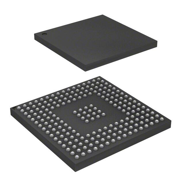


 工商网监
湘ICP备2023018690号
工商网监
湘ICP备2023018690号
