FemtoClock® NG Crystal-to-HCSL
Clock Generator
841654
DATASHEET
GENERAL DESCRIPTION
FEATURES
The 841654 is an optimized PCIe and sRIO clock generator.
The device uses a 25MHz parallel crystal to generate 100MHz
and 125MHz clock signals, replacing solutions requiring multiple
oscillator and fanout buffer solutions. The device has excellent phase
jitter (< 1ps rms) suitable to clock components requiring precise and
low-jitter PCIe or sRIO or both clock signals. Designed for telecom,
networking and industrial applications, the 841654 can also drive the
high-speed sRIO and PCIe SerDes clock inputs of communication
processors, DSPs, switches and bridges.
• Four differential HCSL clock outputs: configurable for PCIe
(100MHz) and sRIO (100MHz or 125MHz) clock signals
One REF_OUT LVCMOS/LVTTL clock output
• Selectable crystal oscillator interface, 25MHz, 18pF parallel resonant crystal or LVCMOS/LVTTL single-ended reference
clock input
• Supports the following output frequencies:
100MHz or 125MHz
• VCO: 500MHz
• PLL bypass and output enable
• RMS phase jitter at 100MHz, using a 25MHz crystal
(1.875MHz - 20MHz): 0.44ps (typical)
• Full 3.3V power supply mode
• -40°C to 85°C ambient operating temperature
• Available in lead-free (RoHS 6) package
BLOCK DIAGRAM
PIN ASSIGNMENT
XTAL_IN
OSC
FemtoClock
PLL
XTAL_OUT
REF_IN Pulldown
1
QA0
1
0
nQA0
0
÷NA
VCO = 500MHz
QA1
nQA1
REF_SEL Pulldown
M = ÷20
QB0
IREF
nQB0
÷NB
BYPASS
QB1
Pulldown
FSEL[0:1] Pulldown
MR/nOE
nQB1
Pulldown
REF_OUT
nREF_OE
Pullup
841654 REVISION A 4/20/15
1
VDD
REF_OUT
GND
QA0
1
2
3
4
nQA0
VDDOA
GND
QA1
nQA1
nREF_OE
BYPASS
REF_IN
REF_SEL
VDDA
5
6
7
8
9
10
11
12
13
14
28
27
26
25
24
23
22
21
20
19
18
17
16
15
IREF
FSEL0
FSEL1
QB0
nQB0
VDDOB
GND
QB1
nQB1
MR/nOE
VDD
XTAL_IN
XTAL_OUT
GND
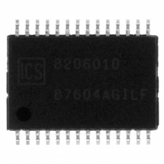
841654
28-Lead TSSOP
6.1mm x 9.7mm x 0.925mm
package body
G Package
Top View
©2015 Integrated Device Technology, Inc.
�841654 DATA SHEET
TABLE 1. PIN DESCRIPTIONS
Number
Name
1, 18
VDD
Power
Type
Core supply pins.
Description
2
REF_OUT
Output
Single-ended reference frequency clock output.
LVCMOS/LVTTL interface levels.
3, 7, 15, 22
GND
Power
Power supply ground.
4, 5,
8, 9
QA0, nQA0,
QA1, nQA1
Ouput
Differential Bank A output pairs. HCSL interface levels.
6
VDDOA
Power
Output supply pin for Bank A outputs.
10
nREF_OE
Input
11
BYPASS
Input
12
REF_IN
Input
13
REF_SEL
Input
14
VDDA
Power
Analog supply pin.
16, 17
XTAL_OUT,
XTAL_IN
Input
Parallel resonant crystal interface. XTAL_OUT is the output,
XTAL_IN is the input. (PLL reference.)
Active low REF_OUT enable/disable. See Table 3E.
LVCMOS/LVTTL interface levels.
Selects PLL operation/PLL bypass operation.
Pulldown
See Table 3C. LVCMOS/LVTTL interface levels.
Single-ended PLL reference clock input.
Pulldown
LVCMOS/LVTTL interface levels.
Reference select. Selects the input reference source.
Pulldown
See Table 3B. LVCMOS/LVTTL interface levels.
Pullup
Active HIGH master reset. Active LOW output enable. When logic HIGH, the
internal dividers are reset and the differential outputs are in high impedance
Pulldown
(HiZ). When logic LOW, the internal dividers and the differential outputs are
enabled. See Table 3D. LVCMOS/LVTTL interface levels.
19
MR/nOE
Input
20, 21
24, 25
nQB1, QB1
nQB0, QB0
Output
Differential Bank B output pairs. HCSL interface levels.
23
VDDOB
Power
Output supply pin for Bank B outputs.
26, 27
FSEL1,
FSEL0
Input
28
IREF
Output
Pulldown Output frequency select pins. LVCMOS/LVTTL interface levels.
HCSL current reference external resistor output. A fixed precision resistor
(RREF = 475Ω) from this pin to ground provides a reference current used
for differential current-mode QA[0:1]/nQA[0:1] and QB[0:1]/nQB[0:1] clock
outputs.
NOTE: Pullup and Pulldown refer to internal input resistors. See Table 2, Pin Characteristics, for typical values.
TABLE 2. PIN CHARACTERISTICS
Symbol
Parameter
CIN
Input Capacitance
4
pF
RPULLUP
Input PullupResistor
51
kΩ
RPULLDOWN
Input Pulldown Resistor
51
kΩ
FEMTOCLOCKS™ CRYSTAL-TO-HCSL
CLOCK GENERATOR
Test Conditions
2
Minimum
Typical
Maximum
Units
REVISION A 4/20/15
�841654 DATA SHEET
TABLE 3A. FSELX FUNCTION TABLE (f
ref
= 25MHZ)
Inputs
Outputs Frequency Settings
FSEL1
FSEL0
M
QA0:1/nQA0:1
QB0:1/nQB0:1
0
0
20
VCO/5 (100MHz)
VCO/5 (100MHz) (default)
0
1
20
VCO/5 (100MHz)
VCO/4 (125MHz)
1
0
20
VCO/5 (100MHz)
QB0:1 = L, nQB0:1 = H
1
1
20
VCO/4 (125MHz)
VCO/4 (125MHz)
TABLE 3B. REF_SEL FUNCTION TABLE
TABLE 3C. BYPASS FUNCTION TABLE
Input
Input
PLL Configuration NOTE 1
REF_SEL
Input Reference
BYPASS
0
XTAL (default)
0
PLL on (default)
1
REF_IN
1
PLL bypassed (QA, QB = fref/N)
NOTE 1: Asynchronous function.
TABLE 3D. MR/nOE FUNCTION TABLE
Input
MR/nOE
FunctionNOTE 1
0
Outputs enabled (default)
1
Device reset, outputs disabled (High Impedance)
NOTE 1: Asynchronous function.
TABLE 3E. nREF_OE FUNCTION TABLE
Input
nREF_OE
FunctionNOTE 1
0
REF_OUT enabled
1
REF_OUT disabled (High Impedance) (default)
NOTE 1: Asynchronous function.
REVISION A 4/20/15
3
FEMTOCLOCKS™ CRYSTAL-TO-HCSL
CLOCK GENERATOR
�841654 DATA SHEET
ABSOLUTE MAXIMUM RATINGS
Supply Voltage, VDD
4.6V
Inputs, VI
-0.5V to VDD + 0.5V
Outputs, VO
-0.5V to VDDOX + 0.5V
Package Thermal Impedance, θJA
64.4°C/W (0 lfpm)
Storage Temperature, TSTG
-65°C to 150°C
N OT E : S t r e s s e s b eyo n d t h o s e l i s t e d u n d e r A b s o l u t e
Maximum Ratings may cause permanent damage to the
device. These ratings are stress specifications only. Functional
operation of product at these conditions or any conditions beyond
those listed in the DC Characteristics or AC Characteristics is not
implied. Exposure to absolute maximum rating conditions for extended periods may affect product reliability.
TABLE 4A. POWER SUPPLY CHARACTERISTICS, VDD = VDDOA = VDDOB = 3.3V±5%, TA = -40°C TO 85°C
Symbol
Parameter
Test Conditions
Minimum
Typical
VDD
Core Supply Voltage
3.135
3.3
3.465
V
VDDA
Analog Supply Voltage
VDD – 0.20
3.3
3.465
V
VDDOA,
VDDOB
Output Supply Voltage
3.135
3.3
3.465
V
IDD
Power Supply Current
Unterminated
85
mA
IDDA
Analog Supply Current
Unterminated
20
mA
IDDOA and
IDDOB
Output Supply Current
Unterminated, RREF = 475 ± 1%
5
mA
Ω
Maximum
Units
TABLE 4B. LVCMOS / LVTTL DC CHARACTERISTICS, VDD = 3.3V±5%, TA = -40°C TO 85°C
Symbol
Parameter
VIH
Input High Voltage
VIL
Input Low Voltage
IIH
IIL
Input High Current
Input Low Current
VOL
Ouput High Voltage;
NOTE 1
Ouput Low Voltage;
NOTE 1
ZOUT
Output Impedance
VOH
Test Conditions
Maximum
Units
2
VDD + 0.3
V
-0.3
0.8
V
Minimum
Typical
REF_IN, REF_SEL,
BYPASS, MR/nOE,
FSEL0, FSEL1
VDD = VIN = 3.465 V
150
µA
nREF_OE
VDD = VIN = 3.465V
5
µA
REF_IN, REF_SEL,
BYPASS, MR/nOE,
FSEL0, FSEL1
VDD = 3.465V, VIN = 0V
-5
µA
nREF_OE
VDD = 3.465V, VIN = 0V
-150
µA
REF_OUT
VDD = 3.465V
2.6
V
REF_OUT
VDD = 3.465V
REF_OUT
VDD = 3.465V
0.5
20
V
Ω
NOTE 1: Outputs terminated with 50Ω to VDD/2. See Parameter Measurement Information Section,
Output Load Test Circuit diagram.
FEMTOCLOCKS™ CRYSTAL-TO-HCSL
CLOCK GENERATOR
4
REVISION A 4/20/15
�841654 DATA SHEET
TABLE 5. CRYSTAL CHARACTERISTICS
Parameter
Test Conditions
Minimum
Mode of Oscillation
Typical
Maximum
Units
Fundamental
Frequency
25
MHz
Equivalent Series Resistance (ESR)
50
Ω
Shunt Capacitance
7
pF
Maximum
Units
NOTE: Characterized using an 18pF parallel resonant crystal.
TABLE 6A. LVCMOS AC CHARACTERISTICS, VDD = 3.3V±5%, TA = -40°C TO 85°C
Symbol
Parameter
f
Output Frequency
t /t
Output Rise/Fall Time
odc
Output Duty Cycle
MAX
R
F
Test Conditions
Minimum
20% to 80%
0.60
1.80
ns
49
51
%
Maximum
Units
REF_OUT
Typical
25
MHz
TABLE 6B. HCSL AC CHARACTERISTICS, VDD = VDDOA = VDDOB = 3.3V±5%, TA = -40°C TO 85°C
Symbol
Parameter
Test Conditions
Output Frequency
f
MAX
tjit(Ø)
RMS Phase Jitter (Random);
NOTE 1
Minimum
Typical
VCO/5
100
MHz
VCO/4
125
MHz
0.44
ps
0.44
ps
100MHz,
(1.875MHz - 20MHz)
125MHz,
(1.875MHz - 20MHz)
tjit(cc)
Cycle-to-Cycle Jitter; NOTE 3
35
ps
tsk(o)
Output Skew;
NOTE 2, 3
100
ps
t
PLL Lock Time
100
ms
L
QAx/nQAx,
QBx/nQBx
V
Voltage High
V
Voltage Low
V
Max. Voltage, Overshoot
V
Min. Voltage, Undershoot
HIGH
LOW
OVS
UDS
125MHz
Ringback Voltage
V
Absolute Crossing Voltage
CROSS
ΔVCROSS
Total Variation of V
t /t
Output Rise/Fall Time
ΔtR /ΔtF
Rise/Fall Time Variation
R
F
700
CROSS
200
over all edges
QAx/nQAx,
QBx/nQBx
measured between
0.175V to 0.525V
100
QAx/nQAx,
48
QBx/nQBx
NOTE: All specifications are taken at 100MHz and 125MHz.
NOTE 1: Please refer to the Phase Noise Plot.
NOTE 2: Defined as skew between outputs at the same supply voltage and with equal load conditions.
Measured at the output differential cross points.
NOTE 3: This parameter is defined in accordance with JEDEC Standard 65.
odc
Output Duty Cycle
REVISION A 4/20/15
950
mV
150
mV
0.3
V
-0.3
V
rb
650
-150
5
V
0.2
V
550
mV
160
mV
700
ps
125
ps
52
%
FEMTOCLOCKS™ CRYSTAL-TO-HCSL
CLOCK GENERATOR
�841654 DATA SHEET
➤
TYPICAL PHASE NOISE AT 100MHZ
Filter
100MHz
Raw Phase Noise Data
➤
➤
NOISE POWER dBc
Hz
RMS Phase Jitter (Random)
1.875MHz to 20MHz = 0.44ps (typical)
Phase Noise Result by adding
a Filter to raw data
OFFSET FREQUENCY (HZ)
➤
TYPICAL PHASE NOISE AT 125MHZ
Filter
125MHz
Raw Phase Noise Data
➤
➤
NOISE POWER dBc
Hz
RMS Phase Jitter (Random)
1.875MHz to 20MHz = 0.44ps (typical)
Phase Noise Result by adding
an Filter to raw data
OFFSET FREQUENCY (HZ)
FEMTOCLOCKS™ CRYSTAL-TO-HCSL
CLOCK GENERATOR
6
REVISION A 4/20/15
�841654 DATA SHEET
PARAMETER MEASUREMENT INFORMATION
3.3V±5%
3.3V±5%
3.3V±5%
3.3V±5%
VDD,
VDDOA,
VDDOB
VDD,
VDDOA, V
DDA
VDDOB
VDDA
HCSL OUTPUT LOAD AC TEST CIRCUIT
HCSL OUTPUT LOAD AC TEST CIRCUIT
3.3V LVCMOS OUTPUT LOAD AC TEST CIRCUIT
RMS PHASE JITTER
nQA[0:1],
nQB[0:1]
QA[0:1],
QB[0:1]
tcycle n
tcycle n+1
tjit(cc) = |tcycle n – tcycle n+1|
1000 Cycles
HCSL OUTPUT SKEW
CYCLE-TO-CYCLE JITTER
REVISION A 4/20/15
7
FEMTOCLOCKS™ CRYSTAL-TO-HCSL
CLOCK GENERATOR
�841654 DATA SHEET
PARAMETER MEASUREMENT INFORMATION, CONTINUED
80%
REF_OUT
80%
20%
20%
tR
tF
LVCMOS OUTPUT RISE/FALL TIME
LVCMOS OUTPUT DUTY CYCLE/PULSE WIDTH/PERIOD
nQAx,
nQBx
0.525V
0.525V
VSW I N G
QAx, QBx
0.175V
0.175V
tR
tF
DIFFERENTIAL MEASUREMENT POINTS FOR RISE/FALL TIME
DIFFERENTIAL MEASUREMENT POINTS FOR DUTY CYCLE/PERIOD
SE MEASUREMENT POINTS FOR DELTA CROSS POINT
DIFFERENTIAL MEASUREMENT POINTS FOR RINGBACK
FEMTOCLOCKS™ CRYSTAL-TO-HCSL
CLOCK GENERATOR
8
REVISION A 4/20/15
�841654 DATA SHEET
PARAMETER MEASUREMENT INFORMATION, CONTINUED
SE MEASUREMENT POINTS FOR ABSOLUTE CROSS POINT/SWING
APPLICATION INFORMATION
POWER SUPPLY FILTERING TECHNIQUES
As in any high speed analog circuitry, the power supply pins
are vulnerable to random noise. To achieve optimum jitter
performance, power supply isolation is required. The 841654
provides separate power supplies to isolate any high switching
noise from the outputs to the internal PLL. VDD, VDDA, VDDOA and
V DDOB should be individually connected to the power supply
plane through vias, and 0.01µF bypass capacitors should be
used for each pin. Figure 1 illustrates this for a generic VDD
pin and also shows that VDDA requires that an additional10Ω
resistor along with a 10µF bypass capacitor be connected to the
VDDA pin.
3.3V
VDD
.01μF
10Ω
VDDA
.01μF
10μF
FIGURE 1. POWER SUPPLY FILTERING
RECOMMENDATIONS FOR UNUSED INPUT AND OUTPUT PINS
OUTPUTS:
INPUTS:
HCSL OUTPUTS
All unused HCSL outputs can be left floating. We recommend that
there is no trace attached. Both sides of the differential output pair
should either be left floating or terminated.
CRYSTAL INPUTS
For applications not requiring the use of the crystal oscillator input,
both XTAL_IN and XTAL_OUT can be left floating. Though not
required, but for additional protection, a 1kΩ resistor can be tied
from XTAL_IN to ground.
LVCMOS OUTPUT
The unused LVCMOS output can be left floating. We recommend
that there is no trace attached.
REF_IN INPUT
For applications not requiring the use of the reference clock,
it can be left floating. Though not required, but for additional
protection, a 1kΩ resistor can be tied from the REF_IN to ground.
LVCMOS CONTROL PINS
All control pins have internal pull-ups or pull-downs; additional
resistance is not required but can be added for additional protection.
A 1kΩ resistor can be used.
REVISION A 4/20/15
9
FEMTOCLOCKS™ CRYSTAL-TO-HCSL
CLOCK GENERATOR
�841654 DATA SHEET
CRYSTAL INPUT INTERFACE
The 841654 has been characterized with 18pF parallel resonant
crystals. The capacitor values shown in Figure 2 below were
determined using a 25MHz, 18pF parallel resonant crystal and were
chosen to minimize the ppm error.
FIGURE 2. CRYSTAL INPUt INTERFACE
LVCMOS TO XTAL INTERFACE
The XTAL_IN input can accept a single-ended LVCMOS signal
through an AC couple capacitor. A general interface diagram
is shown in Figure 3. The XTAL_OUT pin can be left floating.
The input edge rate can be as slow as 10ns. For LVCMOS inputs,
it is recommended that the amplitude be reduced from full swing
to half swing in order to prevent signal interference with the power
rail and to reduce noise. This configuration requires that the output
impedance of the driver (Ro) plus the series resistance (Rs) equals
the transmission line impedance. In addition, matched termination
at the crystal input will attenuate the signal in half. This can be done
in one of two ways. First, R1 and R2 in parallel should equal the
transmission line impedance. For most 50Ω applications, R1 and
R2 can be 100Ω. This can also be accomplished by removing R1
and making R2 50Ω.
VDD
VCC
VDD
VCC
R1
Ro
.1uf
Rs
Zo = 50
Zo = Ro + Rs
XTAL_IN
R2
XTAL_OUT
FIGURE 3. GENERAL DIAGRAM FOR LVCMOS DRIVER TO XTAL INPUT INTERFACE
FEMTOCLOCKS™ CRYSTAL-TO-HCSL
CLOCK GENERATOR
10
REVISION A 4/20/15
�841654 DATA SHEET
SCHEMATIC LAYOUT
for optimizing frequency accuracy. One example of HCSL
and one example of LVCMOS terminations are shown in this
schematic. The decoupling capacitors should be located as
close as possible to the power pin.
Figure 4 shows an example of 841654 application schematic.
In this example, the device is operated at VCC = 3.3V. The 18pF
parallel resonant 25MHz crystal is used. The C1 = 27pF and
C2 = 27pF are recommended for frequency accuracy. For
different board layout, the C1 and C2 may be slightly adjusted
R1
33
Zo = 50
REF_OUT
LVCMOS
R2
33
Zo = 50
+
TL2
VDD
R4
475
R5
33
Zo = 50
-
VDD
TL3
U1
C5
0.1u
R6
50
1
2
3
4
5
6
7
8
9
10
11
12
13
14
VDDOA
VCCOA
C7
.1uf
nREF_OE
BY PASS
REF_SEL
VDD
REF_OUT
GND
QA0
nQA0
VDDOA
GND
QA1
nQA1
nREF_OE
BY PASS
REF_IN
REF_SEL
VDDA
IREF
FSEL0
FSEL1
QB0
nQB0
VDDOB
GND
QB1
nQB1
MR/nOE
VDD
XTAL_IN
XTAL_OUT
GND
28
27
26
25
24
23
22
21
20
19
18
17
16
15
VDDOB
VCCOB
C8
.1uf
MR/nOE VDD
VDD=3.3V
VDDOA=3.3V
HCSL Termination
VDDOB=3.3V
VDD
C6
0.1u
R8
10
Using for PCI Express
Add-In Card
FSEL0
FSEL1
VDD
VDD
R7
50
Zo = 50
+
VDDA
ICS841654I
C1
0.1u
TL4
Zo = 50
C2
10u
-
TL5
C3
27pF
X1
25MHz
18pF
R12
50
R13
50
Logic Control Input Examples
Set Logic
Input to
'1'
VDD
RU1
1K
Set Logic
Input to
'0'
VDD
C4
27pF
RU2
Not Install
To Logic
Input
pins
RD1
Not Install
To Logic
Input
pins
RD2
1K
FIGURE 4. 841654 SCHEMATIC LAYOUT
REVISION A 4/20/15
11
FEMTOCLOCKS™ CRYSTAL-TO-HCSL
CLOCK GENERATOR
Using for PCI Express
Point-to-Point
Connection
�841654 DATA SHEET
POWER CONSIDERATIONS
This section provides information on power dissipation and junction temperature for the 841654.
Equations and example calculations are also provided.
1. Power Dissipation.
The total power dissipation for the 841654 is the sum of the core power plus the power dissipated in the load(s).
The following is the power dissipation for VDD = 3.3V + 5% = 3.465V, which gives worst case results.
NOTE: Please refer to Section 3 for details on calculating power dissipated in the load.
•
•
Power (core)MAX = VDD_MAX * IDD_MAX = 3.465V * 85mA = 294.5mW
Power (outputs)MAX = 50.06mW/Loaded Output pair
If all outputs are loaded, the total power is 4 * 50.06mW = 200.24mW
Total Power_MAX (3.465V, with all outputs switching) = 294.5mW + 200.24mW = 494.74mW
2. Junction Temperature.
Junction temperature, Tj, is the temperature at the junction of the bond wire and bond pad and directly affects the reliability of the
device. The maximum recommended junction temperature for HiPerClockSTM devices is 125°C.
The equation for Tj is as follows: Tj = θJA * Pd_total + TA
Tj = Junction Temperature
θJA = Junction-to-Ambient Thermal Resistance
Pd_total = Total Device Power Dissipation (example calculation is in Section 1 above)
TA = Ambient Temperature
In order to calculate junction temperature, the appropriate junction-to-ambient thermal resistance θJA must be used. Assuming no air flow
and a multi-layer board, the appropriate value is 64.5°C/W per Table 7 below.
Therefore, Tj for an ambient temperature of 85°C with all outputs switching is:
85°C + 0.495W * 64.5°C/W = 116.9°C. This is below the limit of 125°C.
This calculation is only an example. Tj will obviously vary depending on the number of loaded outputs, supply voltage, air flow,
and the type of board (single layer or multi-layer).
TABLE 7. THERMAL RESISTANCE θJA FOR 28-LEAD TSSOP, FORCED CONVECTION
θJA by Velocity (Meters per Second)
0
Multi-Layer PCB, JEDEC Standard Test Boards
FEMTOCLOCKS™ CRYSTAL-TO-HCSL
CLOCK GENERATOR
64.5°C/W
12
1
2.5
60.4°C/W
58.5°C/W
REVISION A 4/20/15
�841654 DATA SHEET
3. Calculations and Equations.
The purpose of this section is to calculate power dissipation on the IC per HCSL output pair.
HCSL output driver circuit and termination are shown in Figure 4.
VDD
IOUT = 17mA
VOUT
RREF =
475 ± 1%
RL
50
IC
FIGURE 4. HCSL DRIVER CIRCUIT AND TERMINATION
HCSL is a current steering output which sources a maximum of 17mA of current per output. To calculate worst case on-chip power
dissipation, use the following equations which assume a 50Ω load to ground.
The highest power dissipation occurs when VDD is HIGH.
Power
= (VDD_HIGH – VOUT ) * IOUT, since VOUT = IOUT * RL
= (VDD_HIGH – IOUT * RL) * IOUT
= (3.465V – 17mA * 50Ω) * 17mA
Total Power Dissipation per output pair = 50.06mW
REVISION A 4/20/15
13
FEMTOCLOCKS™ CRYSTAL-TO-HCSL
CLOCK GENERATOR
�841654 DATA SHEET
RECOMMENDED TERMINATION
Figure 5A is the recommended termination for applications which
require the receiver and driver to be on a separate PCB. All traces
should be 50Ω impedance.
FIGURE 5A. RECOMMENDED TERMINATION
Figure 5B is the recommended termination for applications which
require a point to point connection and contain the driver and
receiver on the same PCB. All traces should all be 50Ω impedance.
FIGURE 5B. RECOMMENDED TERMINATION
FEMTOCLOCKS™ CRYSTAL-TO-HCSL
CLOCK GENERATOR
14
REVISION A 4/20/15
�841654 DATA SHEET
RELIABILITY INFORMATION
TABLE 8. θJAVS. AIR FLOW TABLE FOR 28 LEAD TSSOP
θJA by Velocity (Meters per Second)
0
Multi-Layer PCB, JEDEC Standard Test Boards
64.5°C/W
1
2.5
60.4°C/W
58.5°C/W
TRANSISTOR COUNT
The transistor count for 841654 is: 2954
PACKAGE OUTLINE AND PACKAGE DIMENSIONS
PACKAGE OUTLINE - G SUFFIX FOR 28 LEAD TSSOP
TABLE 9. PACKAGE DIMENSIONS
SYMBOL
Millimeters
Minimum
N
Maximum
28
A
--
1.20
A1
0.05
0.15
A2
0.80
1.05
b
0.19
0.30
c
0.09
0.20
D
9.60
E
E1
9.80
8.10 BASIC
6.00
e
6.20
0.65 BASIC
L
0.45
0.75
α
0°
8°
aaa
--
0.10
Reference Document: JEDEC Publication 95, MO-153
REVISION A 4/20/15
15
FEMTOCLOCKS™ CRYSTAL-TO-HCSL
CLOCK GENERATOR
�841654 DATA SHEET
TABLE 10. ORDERING INFORMATION
Part/Order Number
Marking
Package
Shipping Packaging
Temperature
ICS841654AGILF
ICS841654AGILF
28 Lead “Lead-Free” TSSOP
tube
-40°C to 85°C
ICS841654AGILFT
ICS841654AGILF
28 Lead “Lead-Free” TSSOP
tape & reel
-40°C to 85°C
NOTE: Parts that are ordered with an “LF” suffix to the part number are the Pb-Free configuration and are RoHS compliant.
FEMTOCLOCKS™ CRYSTAL-TO-HCSL
CLOCK GENERATOR
16
REVISION A 4/20/15
�841654 DATA SHEET
REVISION HISTORY SHEET
Rev
A
REVISION A 4/20/15
Table
T10
Page
16
Description of Change
Ordering Information - removed leaded devices.
Updated data sheet format.
17
FEMTOCLOCKS™ CRYSTAL-TO-HCSL
CLOCK GENERATOR
Date
4/20/15
�Corporate Headquarters
6024 Silver Creek Valley Road
San Jose, California 95138
Sales
800-345-7015 or +408-284-8200
Fax: 408-284-2775
www.IDT.com
Technical Support
email: clocks@idt.com
DISCLAIMER Integrated Device Technology, Inc. (IDT) and its subsidiaries reserve the right to modify the products and/or specifications described herein at any time and at IDT’s sole discretion. All information in
this document, including descriptions of product features and performance, is subject to change without notice. Performance specifications and the operating parameters of the described products are determined
in the independent state and are not guaranteed to perform the same way when installed in customer products. The information contained herein is provided without representation or warranty of any kind, whether express or implied, including, but not limited to, the suitability of IDT’s products for any particular purpose, an implied warranty of merchantability, or non-infringement of the intellectual property rights of others.
This document is presented only as a guide and does not convey any license under intellectual property rights of IDT or any third parties.
IDT’s products are not intended for use in applications involving extreme environmental conditions or in life support systems or similar devices where the failure or malfunction of an IDT product can be reasonably expected to significantly affect the health or safety of users. Anyone using an IDT product in such a manner does so at their own risk, absent an express, written agreement by IDT.
Integrated Device Technology, IDT and the IDT logo are registered trademarks of IDT. Other trademarks and service marks used herein, including protected names, logos and designs, are the property of IDT or
their respective third party owners.
Copyright 2015. All rights reserved.
�IMPORTANT NOTICE AND DISCLAIMER
RENESAS ELECTRONICS CORPORATION AND ITS SUBSIDIARIES (“RENESAS”) PROVIDES TECHNICAL
SPECIFICATIONS AND RELIABILITY DATA (INCLUDING DATASHEETS), DESIGN RESOURCES (INCLUDING
REFERENCE DESIGNS), APPLICATION OR OTHER DESIGN ADVICE, WEB TOOLS, SAFETY INFORMATION, AND
OTHER RESOURCES “AS IS” AND WITH ALL FAULTS, AND DISCLAIMS ALL WARRANTIES, EXPRESS OR IMPLIED,
INCLUDING, WITHOUT LIMITATION, ANY IMPLIED WARRANTIES OF MERCHANTABILITY, FITNESS FOR A
PARTICULAR PURPOSE, OR NON-INFRINGEMENT OF THIRD PARTY INTELLECTUAL PROPERTY RIGHTS.
These resources are intended for developers skilled in the art designing with Renesas products. You are solely responsible
for (1) selecting the appropriate products for your application, (2) designing, validating, and testing your application, and (3)
ensuring your application meets applicable standards, and any other safety, security, or other requirements. These
resources are subject to change without notice. Renesas grants you permission to use these resources only for
development of an application that uses Renesas products. Other reproduction or use of these resources is strictly
prohibited. No license is granted to any other Renesas intellectual property or to any third party intellectual property.
Renesas disclaims responsibility for, and you will fully indemnify Renesas and its representatives against, any claims,
damages, costs, losses, or liabilities arising out of your use of these resources. Renesas' products are provided only subject
to Renesas' Terms and Conditions of Sale or other applicable terms agreed to in writing. No use of any Renesas resources
expands or otherwise alters any applicable warranties or warranty disclaimers for these products.
(Rev.1.0 Mar 2020)
Corporate Headquarters
Contact Information
TOYOSU FORESIA, 3-2-24 Toyosu,
Koto-ku, Tokyo 135-0061, Japan
www.renesas.com
For further information on a product, technology, the most
up-to-date version of a document, or your nearest sales
office, please visit:
www.renesas.com/contact/
Trademarks
Renesas and the Renesas logo are trademarks of Renesas
Electronics Corporation. All trademarks and registered
trademarks are the property of their respective owners.
© 2020 Renesas Electronics Corporation. All rights reserved.
�


 工商网监
湘ICP备2023018690号
工商网监
湘ICP备2023018690号
