PRELIMINARY
ICS841S012I
CRYSTAL-TO-0.7V DIFFERENTIAL HCSL/
LVCMOS FREQUENCY SYNTHESIZER
GENERAL DESCRIPTION
FEATURES
The ICS841S012I is an optimized PCIe, sRIO and
ICS
Gigabit Ethernet Frequency Synthesizer and a
HiPerClockS™ member of HiperClock s™ family of high performance clock solutions from IDT. The ICS841S012I
uses a 25MHz parallel resonant crystal to generate 33.33MHz - 200MHz clock signals, replacing solutions
requiring multiple oscillator and fanout buffer solution. The
device supports ±0.25% center-spread, and -0.5% downspread clocking with two spread select pins (SSC[1:0]). The
VCO operates at frequency of 2GHz. The device has three
output banks: Bank A with two HCSL outputs, 100MHz –
250MHz; Bank B with seven 33.33MHz – 200MHz LVCMOS/
LVTTL outputs; and Bank C with one 33.33MHz – 200MHz
LVCMOS/LVTTL output.
• Two 0.7V differential HCSL outputs (Bank A), configurable for
PCIe (100MHz or 250MHz) and sRIO (100MHz or 125MHz)
clock signals
Eight LVCMOS/LVTTL outputs (Banks B/C),
15Ω typical output impedance
Two REF_OUT LVCMOS/LVTTL clock outputs,
20Ω typical output impedance
• Selectable crystal oscillator interface, 25MHz, 18pF parallel
resonant crystal or one LVCMOS/LVTTL single-ended
reference clock input
• Supports the following output frequencies:
HCSL Bank A: 100MHz, 125MHz, 200MHz and 250MHz
LVCMOS/LVTTL Bank B/C: 33.33MHz, 50MHz, 66.67MHz,
100MHz, 125MHz, 133.33MHz, 166.67MHz and 200MHz
All Banks A, B and C have their own dedicated frequency
select pins and can be independently set for the frequencies
mentioned above. The low jitter character istic of the
ICS841S012I makes it an ideal clock source for PCIe, sRIO
and Gigabit Ethernet applications. Designed for networking and
industrial applications, the ICS841S012I can also drive the highspeed clock inputs of communication processors, DSPs,
switches and bridges.
• VCO: 2GHz
• Spread spectrum clock: ±0.25% center-spread and
-0.5% down-spread
• PLL bypass and output enable
• RMS period jitter: 15ps (typical), QB outputs
• Full 3.3V supply mode
• -40°C to 85°C ambient operating temperature
• Available in both standard (RoHS 5) and lead-free (RoHS 6)
packages
VDDOB
VDDOB
QB6
GND
QB5
VDDOB
QB4
GND
QB3
VDDOB
QB2
GND
QB1
QB0
PIN ASSIGNMENT
56 55 54 53 52 51 50 49 48 47 46 45 44 43
42
VDD
REF_OUT0
1
2
REF_OUT1
GND
GND
3
4
5
6
7
8
9
10
11
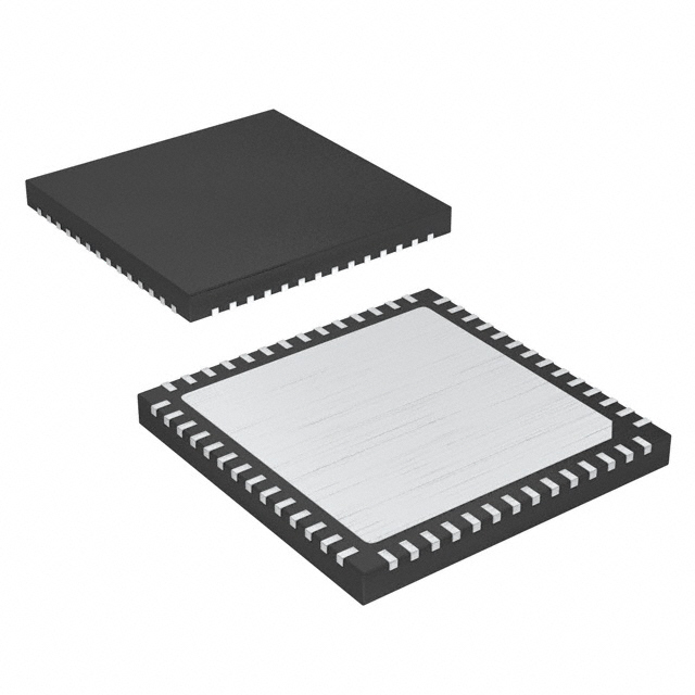
56-Lead VFQFN
8mm x 8mm x 0.925mm
package body
K Package
Top View
37
36
35
34
33
32
31
30
29
VDDOC
QC
GND
QBC_OE
VDDA
VDDA
GND
GND
IREF
QA0
nQA0
QA1
nQA1
VDD
GND
VDD
F_SELB2
F_SELB1
F_SELB0
F_SELC2
F_SELC1
F_SELC0
F_SELA1
F_SELA0
QA_OE
12
13
14
15 16 17 18 19 20 21 22 23 24 25 26 27 28
GND
REF_OE
nMR
VDD
40
39
38
ICS841S012I
SSC1
SSC0
REF_IN
VDD
REF_SEL
XTAL_IN
XTAL_OUT
BYPASS
41
The Preliminary Information presented herein represents a product in pre-production. The noted characteristics are based on initial product characterization
and/or qualification. Integrated Device Technology, Incorporated (IDT) reserves the right to change any circuitry or specifications without notice.
IDT ™ / ICS™ 0.7V HCSL/LVCMOS FREQUENCY SYNTHESIZER
1
ICS841S012BKI REV. A MAY 1, 2008
�ICS841S012I
CRYSTAL-TO-0.7V DIFFERENTIAL HCSL/LVCMOS FREQUENCY SYNTHESIZER
PRELIMINARY
BLOCK DIAGRAM
QA_OE
Pullup
F_SELA[1:0]
Pulldown
BYPASS
Pulldown
2
QA0
nQA0
÷NA
25MHz
XTAL_IN
OSC
nQA1
1
0
PLL
VCO
XTAL_OUT
QB0
2GHz
REF_IN
Pulldown
REF_SEL
Pulldown
QA1
0
1
QB1
QB2
M = ÷80
QB3
÷NB
QB4
F_SELB[2:0]
Pulldown
3
QB5
IREF
QB6
÷NC
F_SELC[2:0]
Pulldown
nMR
Pullup
QBC_OE
Pullup
SSC[1:0]
Pullup
QC
3
2
Spread
Spectrum
REF_OUT0
REF_OUT1
REF_OE
Pulldown
IDT ™ / ICS™ 0.7V HCSL/LVCMOS FREQUENCY SYNTHESIZER
2
ICS841S012BKI REV. A MAY 1, 2008
�ICS841S012I
CRYSTAL-TO-0.7V DIFFERENTIAL HCSL/LVCMOS FREQUENCY SYNTHESIZER
PRELIMINARY
TABLE 1. PIN DESCRIPTIONS
Number
1, 7, 14, 28,
29
2,
3
4, 5, 15, 27,
35, 36, 40,
46, 50, 54
6
Name
Type
Description
VDD
Power
Core supply pins.
REF_OUT0,
REF_OUT1
Output
Single-ended LVCMOS/LVTTL reference clock outputs.
20Ω typical output impedance.
GND
Power
Power supply ground.
REF_IN
Input
8
REF_SEL
Input
9,
10
XTAL_IN,
XTAL_OUT
Input
11
BYPASS
Input
12
REF_OE
Input
13
nMR
Input
16,
17
18,
19,
20
21,
22,
23
24,
25
SSC1,
SSC0
F_SELB2,
F_SELB1,
F_SELB0
F_SELC2,
F_SELC1,
F_SELC0
F_SELA1,
F_SELA0
26
Pulldown Single-ended LVCMOS/LVTTL reference clock input.
Reference select pin. When HIGH selects REF_IN. When LOW,
Pulldown
selects crystal. LVCMOS/LVTTL interface levels. See Table 3E.
Crystal oscillator interface. XTAL_OUT is the output.
XTAL_IN is the input.
When HIGH bypasses PLL. When LOW, selects N divider.
Pulldown
LVCMOS/LVTTL interface levels.
Active HIGH REF_OUT enables/disables pin.
Pulldown
LVCMOS/LVTTL interface levels. See Table 3H.
Active LOW Master Reset. When logic LOW, the internal dividers
are reset and the outputs are in high impedance (HI-Z). When logic
Pullup
HIGH, the internal dividers and the outputs are enabled.
LVCMOS/LVTTL interface levels.
Input
Pullup
SSC control pin. LVCMOS/LVTTL interface levels. See Table 3D.
Input
Pulldown
Frequency select pins for QBx outputs. See Table 3B.
LVCMOS/LVTTL interface levels.
Input
Pulldown
Frequency select pins for QC output. See Table 3C.
LVCMOS/LVTTL interface levels.
Input
Pulldown
QA_OE
Input
Pullup
30, 31
32, 33
nQA1, QA1
nQA0, QA
Output
34
IREF
Output
37, 38
VDDA
Power
39
QBC_OE
Input
41
QC
Output
42
VDDOC
Power
Frequency select pins for QAx/nQAx outputs. See Table 3A.
LVCMOS/LVTTL interface levels.
Output enable pin for Bank A outputs.
LVCMOS/LVTTL interface levels. See Table 3F.
Differential Bank A clock outputs. HCSL interface levels.
Pullup
External fixed precision resistor (475Ω) from this pin to ground
provides a reference current used for differential current-mode
QAx/nQAx clock outputs.
Analog supply pin.
Output enable pin for Bank B and Bank C outputs.
LVCMOS/LVTTL Interface levels. See Table 3G.
Single-ended Bank C clock output. LVCMOS/LVTTL interface levels.
15Ω typical output impedance.
Output supply pin for QC LVCMOS output.
43, 48, 52, 56
VDDOB
Power
Output supply pins for QBx LVCMOS outputs.
44, 45,
QB0, QB1,
Single-ended Bank B clock outputs. LVCMOS/LVTTL interface
47, 49,
QB2, QB3,
Output
levels. 15Ω typical output impedance.
51, 53, 55
QB4, QB5, QB6
NOTE: Pullup and Pulldown refer to internal input resistors. See Table 2, Pin Characteristics, for typical values.
IDT ™ / ICS™ 0.7V HCSL/LVCMOS FREQUENCY SYNTHESIZER
3
ICS841S012BKI REV. A MAY 1, 2008
�ICS841S012I
CRYSTAL-TO-0.7V DIFFERENTIAL HCSL/LVCMOS FREQUENCY SYNTHESIZER
PRELIMINARY
TABLE 2. PIN CHARACTERISTICS
Symbol
Parameter
CIN
Input Capacitance
Test Conditions
CPD
Power Dissipation
Capacitance
QB[0:6], QC
Minimum
VDD, VDDOB, VDDOC = 3.465V
Typical
Maximum
Units
4
pF
9
pF
RPULLUP
Input Pullup Resistor
51
kΩ
RPULLDOWN
Input Pulldown Resistor
51
kΩ
ROUT
Output Impedance
QB[0:6], QC
15
Ω
REF_OUT[1:0]
20
Ω
TABLE 3A. F_SELA FREQUENCY SELECT FUNCTION TABLE
Inputs
Output Frequency (25MHz Ref.)
F_SELA1
F_SELA0
M Divider Value
NA Divider Value
QA[0:1]/nQA[0:1] (MHz)
L
L
80
20
100
L
H
80
16
125
H
L
80
10
200
H
H
80
8
250
TABLE 3B. F_SELB FREQUENCY SELECT FUNCTION TABLE
Inputs
Output Frequency (25MHz Ref.)
F_SELB2
F_SELB1
F_SELB0
M Divider Value
NB Divider Value
QB[0:6] (MHz)
L
L
L
80
60
33.33
L
L
H
80
40
50
L
H
L
80
30
66.67
L
H
H
80
20
100
H
L
L
80
16
125
H
L
H
80
15
133.33
H
H
L
80
12
166.67
H
H
H
80
10
200
TABLE 3C. F_SELC FREQUENCY SELECT FUNCTION TABLE
Inputs
F_SELC2
F_SELC1
L
L
Output Frequency (25MHz Ref.)
F_SELC0
M Divider Value
NC Divider Value
QC (MHz)
L
L
L
H
80
60
33.33
80
40
50
L
H
L
80
30
66.67
L
H
H
H
80
20
100
L
L
80
16
125
H
L
H
80
15
133.33
H
H
L
80
12
166.67
H
H
H
80
10
200
IDT ™ / ICS™ 0.7V HCSL/LVCMOS FREQUENCY SYNTHESIZER
4
ICS841S012BKI REV. A MAY 1, 2008
�ICS841S012I
CRYSTAL-TO-0.7V DIFFERENTIAL HCSL/LVCMOS FREQUENCY SYNTHESIZER
TABLE 3D. SSC FUNCTION TABLE
TABLE 3E. REF_SEL FUNCTION TABLE
Input
Input
SSC1
0
SSC0
0
Mode
0 to -0.5% Down-spread
0
1
±0.25% Center-spread
1
0
±0.25% Center-spread
1
1
SSC Off (default)
TABLE 3F. QA_OE FUNCTION TABLE
REF_SEL
0
Input Reference
1
REF_IN
1
XTAL
TABLE 3G. QBC_OE FUNCTION TABLE
Input
QA_OE
0
PRELIMINARY
Input
Function
QBC_OE
0
QA[0:1]/nQA[0:1] disabled (Hi-Z)
QA[0:1]/nQA[0:1] enabled
1
TABLE 3H. REF_OE FUNCTION TABLE
Function
QB[0:6] and QC disabled (Hi-Z)
QB[0:6] and QC enabled
TABLE 3I. nMR FUNCTION TABLE
Input
REF_OE
0
1
Input
Function
nMR
0
REF_OUT[0:1] disabled (Hi-Z)
REF_OUT[0:1] enabled
IDT ™ / ICS™ 0.7V HCSL/LVCMOS FREQUENCY SYNTHESIZER
Function
Device reset, output divider disabled (Hi-Z)
1
Output enabled
NOTE: This device requires a reset signal after power-up to
function properly.
5
ICS841S012BKI REV. A MAY 1, 2008
�ICS841S012I
CRYSTAL-TO-0.7V DIFFERENTIAL HCSL/LVCMOS FREQUENCY SYNTHESIZER
PRELIMINARY
ABSOLUTE MAXIMUM RATINGS
Supply Voltage, VDD
4.6V
Inputs, VI
-0.5V to VDD + 0.5 V
Outputs, VO
-0.5V to VDDO + 0.5V
NOTE: Stresses beyond those listed under Absolute
Maximum Ratings may cause per manent damage to the
device. These ratings are stress specifications only. Functional operation of product at these conditions or any conditions beyond
those listed in the DC Characteristics or AC Characteristics is not
implied. Exposure to absolute maximum rating conditions for extended periods may affect product reliability.
Package Thermal Impedance, θJA 31.4°C/W (0 mps)
Storage Temperature, TSTG
-65°C to 150°C
TABLE 4A. POWER SUPPLY DC CHARACTERISTICS, VDD = VDDOB = VDDOC = 3.3V±5%, TA = -40°C TO 85°C
Symbol
VDD
Parameter
Core Supply Voltage
Test Conditions
Minimum
3.135
Typical
3.3
Maximum
3.465
Units
V
VDDA
Analog Supply Voltage
VDD – 0.20
3.3
VDD
V
VDDOB, VDDOC
Output Supply Voltage
3.135
3.3
3.465
V
IDD
Power Supply Current
250
mA
IDDA
Analog Supply Current
20
mA
TABLE 4B. LVCMOS/LVTTL DC CHARACTERISTICS, VDD = VDDOB = VDDOC = 3.3V±5%, TA = -40°C TO 85°C
Symbol Parameter
Maximum
Units
VIH
Input High Voltage
2
VDD + 0.3
V
VIL
Input Low Voltage
-0.3
0.8
V
VDD = VIN = 3.465V
5
µA
VDD = VIN = 3.465V
150
µA
IIH
IIL
Input
High Current
Input
Low Current
Test Conditions
QA_OE, QBC_OE,
nMR, SSC0, SSC1,
F_SELA[0:1],
F_SELB[0:2].
F_SELC[0:2],
REF_OE, BYPASS,
REF_IN, REF_SEL
Minimum Typical
QA_OE, QBC_OE,
nMR, SSC0, SSC1,
VDD = 3.465V, VIN = 0V
-150
µA
F_SELA[0:1],
F_SELB[0:2].
F_SELC[0:2],
REF_OE, BYPASS,
REF_IN, REF_SEL
VDD = 3.465V, VIN = 0V
-5
µA
2.6
V
VOH
Output High Voltage; NOTE 1
VDDOB, VDDOC = 3.3V ± 5%
VOL
Output Low Voltage; NOTE 1
VDDOB, VDDOC = 3.3V ± 5%
0.5
V
NOTE 1: Outputs terminated with 50Ω to VDDOB, C/2. See Parameter Measurement Information,
Output Load Test Circuit diagram.
IDT ™ / ICS™ 0.7V HCSL/LVCMOS FREQUENCY SYNTHESIZER
6
ICS841S012BKI REV. A MAY 1, 2008
�ICS841S012I
CRYSTAL-TO-0.7V DIFFERENTIAL HCSL/LVCMOS FREQUENCY SYNTHESIZER
PRELIMINARY
TABLE 5. CRYSTAL CHARACTERISTICS
Parameter
Test Conditions
Minimum
Mode of Oscillation
Typical
Maximum
Units
Fundamental
Frequency
25
Equivalent Series Resistance (ESR)
MHz
50
Shunt Capacitance
Drive Level
Ω
7
pF
100
µW
Maximum
Units
200
MHz
NOTE: Characterized using an 18pF parallel resonant cr ystal.
TABLE 6. AC CHARACTERISTICS, VDD = VDDOB = VDDOC = 3.3V±5%, TA = -40°C TO 85°C
Symbol
Parameter
Test Conditions
QB[0:6]
fOUT
Output Frequency
QA[0:1]/nQA[0:1]
100
250
MHz
33.33
200
MHz
QB[0:6]
35
ps
QA[0:1]/nQA[0:1]
10
ps
50
ps
tsk(o)
Output Skew;
NOTE 1, 2
tsk(b)
Bank Skew; NOTE 2, 3
tjit(cc)
Cycle-to-Cycle
Jitter ; NOTE 2
RMS Period Jitter
across Banks B and C
QA[0:1]/nQA[0:1]
45
ps
QB[0:6]
55
ps
QC
50
ps
QA[0:1]/nQA[0:1]
7
ps
QB[0:6], QC
15
ps
VHIGH
SSC Modulation
Frequency
Voltage High
VLOW
Voltage Low
-150
VCROSS
Absolute Crossing Voltage
250
ΔVCROSS
Total Variation of VCROSS over all edges
FM
tR / tF
Output
Rise/Fall Time
Typical
33.33
QC
tjit(per)
Minimum
Banks A, B, C
Bank A
Banks B, C
measured between
0.175V to 0.525V
20% - 80%
29
33.33
kHz
660
850
mV
mV
175
550
mV
140
mV
700
ps
350
Bank A
45
55
Banks B, C
50
NOTE 1: Defined as skew between outputs at the same supply voltages and with equal load conditions.
Measured at VDDOB, C/2.
NOTE 2: This parameter is defined in accordance with JEDEC Standard 65.
NOTE 3: Defined as skew within a bank of outputs at the same supply voltage and with equal load conditions.
odc
Output Duty Cycle
IDT ™ / ICS™ 0.7V HCSL/LVCMOS FREQUENCY SYNTHESIZER
7
ps
%
%
ICS841S012BKI REV. A MAY 1, 2008
�ICS841S012I
CRYSTAL-TO-0.7V DIFFERENTIAL HCSL/LVCMOS FREQUENCY SYNTHESIZER
PRELIMINARY
PARAMETER MEASUREMENT INFORMATION
3.3V±5%
1.65V±5%
3.3V±5%
1.65V±5%
VDD,
VDDOB,
VDDOC
SCOPE
VDD
33Ω
100Ω
Measurement
Point
100Ω
Measurement
Point
VDDA
VDDA
49.9Ω
Qx
2pF
HCSL
LVCMOS
33Ω
GND
GND
49.9Ω
2pF
475Ω
IREF
-1.65V±5%
0V
3.3V CORE/3.3V LVCMOS OUTPUT LOAD AC TEST CIRCUIT
3.3V CORE/3.3V HCSL OUTPUT LOAD AC TEST CIRCUIT
nQx
V
DDOX
Qx
Qx
2
nQy
V
DDOX
Qy
Qy
2
tsk(o)
tsk(o)
LVCMOS OUTPUT SKEW
HCSL OUTPUT SKEW
Rise Edge Rate
80%
Fall Edge Rate
+150mV
80%
0.0V
-150mV
20%
20%
QC,
QB0:QB6,
REF_OUT0,
REF_OUT1
Q - nQ
tR
tF
DIFFERENTIAL MEASUREMENT POINTS FOR RISE/FALL TIME
LVCMOS OUTPUT RISE/FALL TIME
IDT ™ / ICS™ 0.7V HCSL/LVCMOS FREQUENCY SYNTHESIZER
8
ICS841S012BKI REV. A MAY 1, 2008
�ICS841S012I
CRYSTAL-TO-0.7V DIFFERENTIAL HCSL/LVCMOS FREQUENCY SYNTHESIZER
PRELIMINARY
PARAMETER MEASUREMENT INFORMATION, CONTINUED
VOH
Qx:Qx
VDDOX
2
VREF
VDDOX
2
Qx:Qx
VOL
1σ contains 68.26% of all measurements
2σ contains 95.4% of all measurements
3σ contains 99.73% of all measurements
4σ contains 99.99366% of all measurements
6σ contains (100-1.973x10⁻⁷)% of all measurements
tsk(b)
Histogram
Reference Point
Mean Period
(Trigger Edge)
(First edge after trigger)
(where X = Bank A or Bank B)
RMS PERIOD JITTER
BANK SKEW
nQA0, nQA1
V
V
DDO
➤
tcycle n+1
➤
➤
tjit(cc) = tcycle n – tcycle n+1
1000 Cycles
V
DDO
2
➤
➤
tcycle n
QC,
QB0:QB6,
REF_OUT0,
REF_OUT1
DDO
2
➤
QA0, QA1
➤
tcycle n
2
tcycle n+1
➤
tjit(cc) = tcycle n – tcycle n+1
1000 Cycles
LVCMOS CYCLE-TO-CYCLE JITTER
DIFFERENTIAL CYCLE-TO-CYCLE JITTER
Clock Period (Differential)
Positive Duty
Cycle (Differential)
Negative Duty
Cycle (Differential)
V
DDOX
QC,
QB0:QB6,
REF_OUT0,
REF_OUT1
2
0.0V
t PW
t
PERIOD
Q - nQ
odc =
t PW
x 100%
t PERIOD
LVCMOS OUTPUT DUTY CYCLE/PULSE WIDTH/PERIOD
IDT ™ / ICS™ 0.7V HCSL/LVCMOS FREQUENCY SYNTHESIZER
DIFFERENTIAL MEASUREMENT POINTS FOR DUTY CYCLE/PERIOD
9
ICS841S012BKI REV. A MAY 1, 2008
�ICS841S012I
CRYSTAL-TO-0.7V DIFFERENTIAL HCSL/LVCMOS FREQUENCY SYNTHESIZER
PARAMETER MEASUREMENT INFORMATION,
PRELIMINARY
CONTINUED
nQ
VCROSS_DELTA = 140mV
Q
SE MEASUREMENT POINTS FOR DELTA CROSS POINT
IDT ™ / ICS™ 0.7V HCSL/LVCMOS FREQUENCY SYNTHESIZER
10
ICS841S012BKI REV. A MAY 1, 2008
�ICS841S012I
CRYSTAL-TO-0.7V DIFFERENTIAL HCSL/LVCMOS FREQUENCY SYNTHESIZER
PRELIMINARY
APPLICATION INFORMATION
POWER SUPPLY FILTERING TECHNIQUES
As in any high speed analog circuitry, the power supply pins are
vulnerable to random noise. To achieve optimum jitter performance, power supply isolation is required. The ICS841S012I provides separate power supplies to isolate any high switching noise
from the outputs to the internal PLL. VDD, VDDA, VDDOB, and VDDOC
should be individually connected to the power supply
plane through vias, and 0.01µF bypass capacitors should be used
for each pin. Figure 1 illustrates this for a generic VDD pin and
also shows that VDDA requires that an additional10Ω resistor
along with a 10µF bypass capacitor be connected to the VDDA pin.
The 10Ω resistor can also be replaced by a ferrite bead.
3.3V
VDD
.01μF
10Ω
VDDA
.01μF
10μF
FIGURE 1. POWER SUPPLY FILTERING
RECOMMENDATIONS FOR UNUSED INPUT AND OUTPUT PINS
INPUTS:
OUTPUTS:
CRYSTAL INPUTS
For applications not requiring the use of the crystal oscillator
input, both XTAL_IN and XTAL_OUT can be left floating. Though
not required, but for additional protection, a 1kΩ resistor can be
tied from XTAL_IN to ground.
LVCMOS OUTPUTS
All unused LVCMOS output can be left floating. We recommend
that there is no trace attached.
DIFFERENTIAL OUTPUT
All unused differential outputs can be left floating. We recommend
that there is no trace attached. Both sides of the differential output
pair should either be left floating or terminated.
REF_IN INPUT
For applications not requiring the use of the reference clock,
it can be left floating. Though not required, but for additional
protection, a 1kΩ resistor can be tied from the REF_IN to ground.
LVCMOS CONTROL PINS
All control pins have internal pull-ups or pull-downs; additional
resistance is not required but can be added for additional
protection. A 1kΩ resistor can be used.
IDT ™ / ICS™ 0.7V HCSL/LVCMOS FREQUENCY SYNTHESIZER
11
ICS841S012BKI REV. A MAY 1, 2008
�ICS841S012I
CRYSTAL-TO-0.7V DIFFERENTIAL HCSL/LVCMOS FREQUENCY SYNTHESIZER
PRELIMINARY
CRYSTAL INPUT INTERFACE
The ICS841S012I has been characterized with 18pF parallel
resonant crystals. The capacitor values shown in Figure 2 below
were determined using a 25MHz, 18pF parallel resonant crystal
and were chosen to minimize the ppm error.
XTAL_IN
C1
X1
Crystal
XTAL_OUT
C2
FIGURE 2. CRYSTAL INPUt INTERFACE
LVCMOS TO XTAL INTERFACE
The XTAL_IN input can accept a single-ended LVCMOS signal
through an AC coupling capacitor. A general interface diagram is
shown in Figure 3. The XTAL_OUT pin can be left floating. The
input edge rate can be as slow as 10ns. For LVCMOS inputs, it is
recommended that the amplitude be reduced from full swing to
half swing in order to prevent signal interference with the power
rail and to reduce noise. This configuration requires that the output
impedance of the driver (Ro) plus the series resistance (Rs) equals
the transmission line impedance. In addition, matched termination
at the crystal input will attenuate the signal in half. This can be
done in one of two ways. First, R1 and R2 in parallel should equal
the transmission line impedance. For most 50Ω applications, R1
and R2 can be 100Ω. This can also be accomplished by removing
R1 and making R2 50Ω.
VDD
VDD
R1
Ro
.1uf
Rs
Zo = 50
Zo = Ro + Rs
XTAL_IN
R2
XTAL_OUT
FIGURE 3. GENERAL DIAGRAM FOR LVCMOS DRIVER TO XTAL INPUT INTERFACE
IDT ™ / ICS™ 0.7V HCSL/LVCMOS FREQUENCY SYNTHESIZER
12
ICS841S012BKI REV. A MAY 1, 2008
�ICS841S012I
CRYSTAL-TO-0.7V DIFFERENTIAL HCSL/LVCMOS FREQUENCY SYNTHESIZER
PRELIMINARY
VFQFN EPAD THERMAL RELEASE PATH
In order to maximize both the removal of heat from the package
and the electrical performance, a land patter n must be
incorporated on the Printed Circuit Board (PCB) within the footprint
of the package corresponding to the exposed metal pad or
exposed heat slug on the package, as shown in Figure 4. The
solderable area on the PCB, as defined by the solder mask, should
be at least the same size/shape as the exposed pad/slug area on
the package to maximize the thermal/electrical performance.
Sufficient clearance should be designed on the PCB between the
outer edges of the land pattern and the inner edges of pad pattern
for the leads to avoid any shorts.
are application specific and dependent upon the package power
dissipation as well as electrical conductivity requirements. Thus,
thermal and electrical analysis and/or testing are recommended
to determine the minimum number needed. Maximum thermal
and electrical performance is achieved when an array of vias is
incorporated in the land pattern. It is recommended to use as
many vias connected to ground as possible. It is also
recommended that the via diameter should be 12 to 13mils (0.30
to 0.33mm) with 1oz copper via barrel plating. This is desirable to
avoid any solder wicking inside the via during the soldering process
which may result in voids in solder between the exposed pad/
slug and the thermal land. Precautions should be taken to
eliminate any solder voids between the exposed heat slug and
the land pattern. Note: These recommendations are to be used
as a guideline only. For further information, refer to the Application
Note on the Surface Mount Assembly of Amkor’s Thermally/
Electrically Enhance Leadfame Base Package, Amkor Technology.
While the land pattern on the PCB provides a means of heat
transfer and electrical grounding from the package to the board
through a solder joint, thermal vias are necessary to effectively
conduct from the surface of the PCB to the ground plane(s). The
land pattern must be connected to ground through these vias.
The vias act as “heat pipes”. The number of vias (i.e. “heat pipes”)
PIN
PIN PAD
SOLDER
EXPOSED HEAT SLUG
GROUND PLANE
SOLDER
LAND PATTERN
THERMAL VIA
PIN
PIN PAD
(GROUND PAD)
FIGURE 4. P.C.ASSEMBLY FOR EXPOSED PAD THERMAL RELEASE PATH –SIDE VIEW (DRAWING NOT TO SCALE)
IDT ™ / ICS™ 0.7V HCSL/LVCMOS FREQUENCY SYNTHESIZER
13
ICS841S012BKI REV. A MAY 1, 2008
�ICS841S012I
CRYSTAL-TO-0.7V DIFFERENTIAL HCSL/LVCMOS FREQUENCY SYNTHESIZER
PRELIMINARY
RECOMMENDED TERMINATION
Figure 5A is the recommended termination for applications
which require the receiver and driver to be on a separate PCB.
All traces should be 50Ù impedance.
FIGURE 5A. RECOMMENDED TERMINATION
Figure 5B is the recommended termination for applications
which require a point to point connection and contain the
driver and receiver on the same PCB. All traces should all be
50Ù impedance.
FIGURE 5B. RECOMMENDED TERMINATION
IDT ™ / ICS™ 0.7V HCSL/LVCMOS FREQUENCY SYNTHESIZER
14
ICS841S012BKI REV. A MAY 1, 2008
�ICS841S012I
CRYSTAL-TO-0.7V DIFFERENTIAL HCSL/LVCMOS FREQUENCY SYNTHESIZER
PRELIMINARY
POWER CONSIDERATIONS
This section provides information on power dissipation and junction temperature for the ICS841S012I.
Equations and example calculations are also provided.
1. Power Dissipation.
The total power dissipation for the ICS841S012I is the sum of the core power plus the power dissipated in the load(s).
The following is the power dissipation for VDD = 3.3V + 5% = 3.465V, which gives worst case results.
Core and HCSL Output Power Dissipation
• Power (core) = VDD_MAX * (IDD + IDDA ) = 3.465V * (250mA + 20mA) = 935.6mW
Power (HCSL) = 44.5mW/Load Output Pair
If all outputs are loaded, the total power is 2 * 44.5mW = 89mW
LVCMOS Output Power Dissipation, ROUT = 15Ω
Ω
•
Output Impedance ROUT Power Dissipation due to Loading 50Ω to VDDO/2
Output Current IOUT = VDDO_MAX / [2 * (50Ω + ROUT)] = 3.465V / [2 * (50Ω + 15Ω)] = 26.7mA
•
Power Dissipation on the ROUT per LVCMOS output
Power (ROUT) = ROUT * (IOUT)2 = 15Ω * (26.7mA)2 = 10.7mW per output
•
Total Power Dissipation on the ROUT
•
Dynamic Power Dissipation at 200MHz
Power (200MHz) = CPD * Frequency * (VDDO)2 = 9pF * 200MHz * (3.465V)2 = 21.6mW per output
Ω ) = 10.7mW * 7 = 74.9mW
Total Power (ROUT = 15Ω
Total Power (200MHz) = 21.6mW * 7 = 151.2mW
LVCMOS Output Power Dissipation, ROUT = 20Ω
Ω
•
Output Impedance ROUT Power Dissipation due to Loading 50Ω to VDDO/2
Output Current IOUT = VDDO_MAX / [2 * (50Ω + ROUT)] = 3.465V / [2 * (50Ω + 20Ω)] = 24.75mA
•
Power Dissipation on the ROUT per LVCMOS output
Power (ROUT) = ROUT * (IOUT)2 = 20Ω * (24.75mA)2 = 12.3mW per output
•
Total Power Dissipation on the ROUT
•
Dynamic Power Dissipation at 25MHz
Power (25MHz) = CPD * Frequency * (VDDO)2 = 9pF * 25MHz * (3.465V)2 = 2.7mW per output
Total Power (ROUT = 20Ω
Ω ) = 12.3mW * 2 = 24.6mW
Total Power (25MHz) = 2.7mW * 2 = 5.4mW
Total Power Dissipation
•
Total Power
= Power (core) + Power (HCSL) + Total Power (ROUT= 15Ω) + Total Power (200MHz) + Total Power (ROUT= 20Ω) +
Total Power (25MHz)
= 935.6mW + 89mW + 74.9mW + 151.2mW + 24.6mW + 5.4mW
= 1280.7mW
IDT ™ / ICS™ 0.7V HCSL/LVCMOS FREQUENCY SYNTHESIZER
15
ICS841S012BKI REV. A MAY 1, 2008
�ICS841S012I
CRYSTAL-TO-0.7V DIFFERENTIAL HCSL/LVCMOS FREQUENCY SYNTHESIZER
PRELIMINARY
2. Junction Temperature.
Junction temperature, Tj, is the temperature at the junction of the bond wire and bond pad and directly affects the reliability
of the device. The maximum recommended junction temperature for HiPerClockSTM devices is 125°C.
The equation for Tj is as follows: Tj = θJA * Pd_total + TA
Tj = Junction Temperature
θJA = Junction-to-Ambient Thermal Resistance
Pd_total = Total Device Power Dissipation (example calculation is in section 1 above)
TA = Ambient Temperature
In order to calculate junction temperature, the appropriate junction-to-ambient thermal resistance θJA must be used.
Assuming 1 meter per second air flow and a multi-layer board, the appropriate value is 27.5°C/W per Table 7.
Therefore, Tj for an ambient temperature of 85°C with all outputs switching is:
85°C + 1.281W * 27.5°C/W = 120.2°C. This is below the limit of 125°C.
This calculation is only an example. Tj will obviously vary depending on the number of loaded outputs, supply voltage, air
flow, and the type of board (single layer or multi-layer).
TABLE 7. THERMAL RESISTANCE θJA FOR 56 LEAD VFQFN, FORCED CONVECTION
θJA by Velocity (Meters per second)
Multi-Layer PCB, JEDEC Standard Test Boards
IDT ™ / ICS™ 0.7V HCSL/LVCMOS FREQUENCY SYNTHESIZER
16
0
1
2.5
31.4°C/W
27.5°C/W
24.6°C/W
ICS841S012BKI REV. A MAY 1, 2008
�ICS841S012I
CRYSTAL-TO-0.7V DIFFERENTIAL HCSL/LVCMOS FREQUENCY SYNTHESIZER
PRELIMINARY
3. Calculations and Equations.
The purpose of this section is to calculate power dissipation on the IC per HCSL output pair.
HCSL output driver circuit and termination are shown in Figure 6.
VDD
IOUT = 17mA
➤
VOUT
RREF =
475Ω ± 1%
RL
50Ω
IC
FIGURE 6. HCSL DRIVER CIRCUIT AND TERMINATION
HCSL is a current steering output which sources a maximum of 17mA of current per output. To calculate worst case on-chip power
dissipation, use the following equations which assume a 50Ω load to ground.
The highest power dissipation occurs at maximum VDD .
Power
= (VDD_MAX – VOUT ) * IOUT, since VOUT = IOUT * RL
= (VDD_MAX – IOUT * RL) * IOUT
= (3.465V – 17mA * 50Ω) * 17mA
Total Power Dissipation per output pair = 44.5mW
IDT ™ / ICS™ 0.7V HCSL/LVCMOS FREQUENCY SYNTHESIZER
17
ICS841S012BKI REV. A MAY 1, 2008
�ICS841S012I
CRYSTAL-TO-0.7V DIFFERENTIAL HCSL/LVCMOS FREQUENCY SYNTHESIZER
PRELIMINARY
RELIABILITY INFORMATION
TABLE 8. θJAVS. AIR FLOW TABLE FOR 56 LEAD VFQFN
θJA by Velocity (Meters per second)
Multi-Layer PCB, JEDEC Standard Test Boards
0
1
2.5
31.4°C/W
27.5°C/W
24.6°C/W
TRANSISTOR COUNT
The transistor count for ICS841S012I is: 11,537
IDT ™ / ICS™ 0.7V HCSL/LVCMOS FREQUENCY SYNTHESIZER
18
ICS841S012BKI REV. A MAY 1, 2008
�ICS841S012I
CRYSTAL-TO-0.7V DIFFERENTIAL HCSL/LVCMOS FREQUENCY SYNTHESIZER
PRELIMINARY
PACKAGE OUTLINE - K SUFFIX FOR 56 LEAD VFQFN
(Ref.)
S eating Plan e
N &N
Even
(N -1)x e
(R ef.)
A1
Ind ex Area
L
A3
N
N
e (Ty p.)
2 If N & N
1
Anvil
Singula tion
are Even
2
OR
E2
(N -1)x e
(Re f.)
E2
2
To p View
b
A
(Ref.)
D
e
D2
2
N &N
Odd
0. 08
Chamfer 4x
0.6 x 0.6 max
OPTIONAL
C
Th er mal
Ba se
D2
C
NOTE: The following package mechanical drawing is a generic
drawing that applies to any pin count VFQFN package. This drawing is not intended to convey the actual pin count or pin layout of
this device. The pin count and pinout are shown on the front page.
The package dimensions are in Table 8 below.
TABLE 9. PACKAGE DIMENSIONS
JEDEC VARIATION
ALL DIMENSIONS IN MILLIMETERS
SYMBOL
MINIMUM
MAXIMUM
56
N
A
0.80
1.0
A1
0
0.05
0.25 Reference
A3
b
0.18
0.30
e
0.50 BASIC
ND
14
NE
14
8.0
D
D2
4.35
4.65
8.0
E
E2
5.05
5.35
L
0.3
0.55
Reference Document: JEDEC Publication 95, MO-220
IDT ™ / ICS™ 0.7V HCSL/LVCMOS FREQUENCY SYNTHESIZER
19
ICS841S012BKI REV. A MAY 1, 2008
�ICS841S012I
CRYSTAL-TO-0.7V DIFFERENTIAL HCSL/LVCMOS FREQUENCY SYNTHESIZER
PRELIMINARY
TABLE 10. ORDERING INFORMATION
Part/Order Number
Marking
Package
Shipping Packaging Temperature
841S012BKI
TBD
56 lead VFQFN
tray
-40°C to 85°C
T BD
56 lead VFQFN
1000 tape & reel
-40°C to 85°C
841S012BKIT
841S012BKILF
ICS841S012BIL
56 lead "Lead-Free" VFQFN
tray
-40°C to 85°C
841S012BKILFT
ICS841S012BIL
56 lead "Lead-Free" VFQFN
1000 tape & reel
-40°C to 85°C
NOTE: Par ts that are ordered with an "LF" suffix to the par t number are the Pb-Free configuration and are RoHS compliant.
While the information presented herein has been checked for both accuracy and reliability, Integrated Device Technology, Incorporated (IDT) assumes no responsibility for either its use or for
infringement of any patents or other rights of third parties, which would result from its use. No other circuits, patents, or licenses are implied. This product is intended for use in normal commercial and
industrial applications. Any other applications such as those requiring high reliability or other extraordinary environmental requirements are not recommended without additional processing by IDT. IDT
reserves the right to change any circuitry or specifications without notice. IDT does not authorize or warrant any IDT product for use in life support devices or critical medical instruments.
IDT ™ / ICS™ 0.7V HCSL/LVCMOS FREQUENCY SYNTHESIZER
20
ICS841S012BKI REV. A MAY 1, 2008
�ICS841S012I
CRYSTAL-TO-0.7V DIFFERENTIAL HCSL/LVCMOS FREQUENCY SYNTHESIZER
PRELIMINARY
Innovate with IDT and accelerate your future networks. Contact:
www.IDT.com
For Sales
For Tech Support
Corporate Headquarters
800-345-7015 (inside USA)
+408-284-8200 (outside USA)
Fax: 408-284-2775
www.IDT.com/go/contactIDT
netcom@idt.com
+480-763-2056
Integrated Device Technology, Inc.
6024 Silver Creek Valley Road
San Jose, CA 95138
United States
800-345-7015 (inside USA)
+408-284-8200 (outside USA)
© 2008 Integrated Device Technology, Inc. All rights reserved. Product specifications subject to change without notice. IDT, the IDT logo, ICS and HiPerClockS are trademarks
of Integrated Device Technology, Inc. Accelerated Thinking is a service mark of Integrated Device Technology, Inc. All other brands, product names and marks are or may be
trademarks or registered trademarks used to identify products or services of their respective owners.
Printed in USA
�


 工商网监
湘ICP备2023018690号
工商网监
湘ICP备2023018690号
