Crystal or Differential to Differential
Clock Fanout Buffer
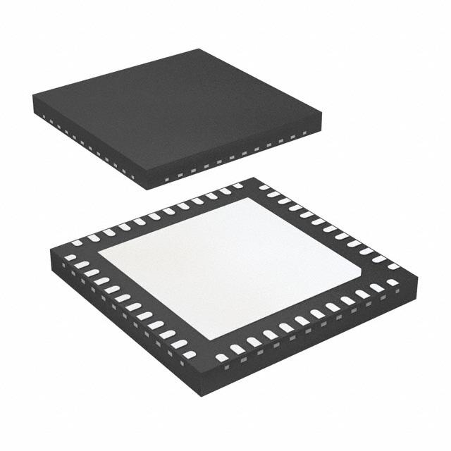
IDT8T3910I
PRELIMINARY DATA SHEET
General Description
Features
The IDT8T3910I is a high-performance clock fanout buffer. The input
clock can be selected from two differential inputs or one crystal input.
The internal oscillator circuit is automatically disabled if the crystal
input is not selected. The selected signal is distributed to ten
differential outputs which can be configured as LVPECL, LVDS or
HSCL outputs. In addition, an LVCMOS output is provided. The user
should always turn off this LVCMOS output when (the) clock is over
200MHz. The differential outputs can be disabled into an
high-impedance state. The device is designed for signal fanout of
high-frequency, low phase-noise clock and data signal. The outputs
are at a defined level when inputs are open or shorted. It’s designed
to operate from a 3.3V core power supply, and either a 3.3V or 2.5V
output operating supply.
•
•
Two differential reference clock input pairs
•
•
•
Crystal Oscillator Interface
•
One single-ended reference output with synchronous enable to
avoid clock glitch
•
Output skew: (Bank A and Bank B at the same output level) 32ps
(typical)
•
•
•
•
Part-to-part skew: 200ps (typical)
•
•
-40°C to 85°C ambient operating temperature
Available in lead-free (RoHS 6) package
Differential input pairs can accept the following differential input
levels: LVPECL, LVDS, HCSL
Crystal input frequency range: 10MHz to 40MHz
Two banks, each has five differential output pairs that can be
configured as LVPECL or LVDS or HCSL
Additive RMS phase jitter: 0.22ps (typical)
Power supply modes:
Output supply voltage modes:
VCC/VDDO
3.3V/3.3V
3.3V/2.5V
The Preliminary Information presented herein represents a product in pre-production. The noted characteristics are based on initial product characterization and/or qualification.
Integrated Device Technology, Incorporated (IDT) reserves the right to change any circuitry or specifications without notice.
IDT8T3910BNLI MARCH 23, 2012
1
©2012 Integrated Device Technology, Inc.
�IDT8T3910I Preliminary Data Sheet
CRYSTAL OR DIFFERNTIAL-TO-DIFFERENTIAL CLOCK FANOUT BUFFER
Block Diagram
SMODEA[1:0]
Pulldown
REF_SEL[1:0]
Pulldown
CLK0
Pulldown
nCLK0
CLK1
nCLK1
Pullup/Pulldown
QA0
nQA0
QA1
nQA1
QA2
nQA2
QA3
nQA3
QA4
nQA4
00
Pulldown
Pullup/Pulldown
XTAL_IN
OSC
XTAL_OUT
01
QB0
nQB0
QB1
nQB1
QB2
nQB2
QB3
nQB3
QB4
nQB4
10
or
11
IREF
SMODEB[1:0]
Pulldown
REFOUT
OE_SE
Pulldown
IDT8T3910BNLI MARCH 23, 2012
SYNC
2
©2012 Integrated Device Technology, Inc.
�IDT8T3910I Preliminary Data Sheet
CRYSTAL OR DIFFERNTIAL-TO-DIFFERENTIAL CLOCK FANOUT BUFFER
QB0
nQB0
QB1
nQB1
VDDO
QB2
nQB2
VDDO
QB3
nQB3
QB4
nQB4
Pin Assignment
36
35
34
33
32
31
30
29
28
27
26
25
GND 37
24 GND
IREF 38
23 SMODEB0
SMODEB1 39
22 REF_SEL1
nCLK1 40
CLK1 41
VDD 42
GND 43
REFOUT 44
21 nCLK0
IDT8T3910I
48 Lead VFQFN
7.0mm x 7.0mm x 0.925mm, package body
NL Package
Top View
VDDO 45
19 REF_SEL0
18 GND
17 OSCO
16 OSCI
OE_SE 46
15 VDD
SMODEA1 47
14 SMODEA0
GND 48
IDT8T3910BNLI MARCH 23, 2012
20 CLK0
5
6
7
8
3
nQA0
QA1
nQA1
VDDO
QA2
nQA2
VDDO
9
10
11
12
QA4
4
nQA4
3
nQA3
2
QA3
1
QA0
13 GND
©2012 Integrated Device Technology, Inc.
�IDT8T3910I Preliminary Data Sheet
CRYSTAL OR DIFFERNTIAL-TO-DIFFERENTIAL CLOCK FANOUT BUFFER
Table 1. Pin Descriptions
Number
Name
1, 2
QA0, nQA0
Output
Type
Description
Differential Bank A clock output pair. LVPECL, LVDS or HCSL interface levels.
3, 4
QA1, nQA1
Output
Differential Bank A clock output pair. LVPECL, LVDS or HCSL interface levels.
5, 8, 29, 32, 45
VDDO
Power
Output supply pins.
6, 7
QA2, nQA2
Output
Differential Bank A clock output pair. LVPECL, LVDS or HCSL interface levels.
9, 10
QA3, nQA3
Output
Differential Bank A clock output pair. LVPECL, LVDS or HCSL interface levels.
11, 12
QA4, nQA4
Output
Differential Bank A clock output pair. LVPECL, LVDS or HCSL interface levels.
13, 18, 24,
37, 43, 48
GND
Power
Power supply ground.
14, 47
SMODEA0,
SMODEA1
Input
15, 42
VDD
Power
16,
17
XTAL_IN,
XTAL_OUT
Input
19,
22
REF_SEL0,
REF_SEL1
Input
Pulldown
Input clock selection. LVCMOS/LVTTL interface levels.
See Table 3A for function.
20
CLK0
Input
Pulldown
Non-inverting differential clock.
21
nCLK0
Input
Pullup/
Pulldown
Inverting differential clock. Internal resistor bias to VDD/2.
23, 39
SMODEB0,
SMODEB1
Input
Pulldown
Output driver select for Bank B outputs. See Table 3D for function.
LVCMOS/LVTTL interface levels.
25, 26
nQB4, QB4
Output
Differential Bank B clock output pair. LVPECL, LVDS or HCSL interface levels.
27, 28
nQB3, QB3
Output
Differential Bank B clock output pair. LVPECL, LVDS or HCSL interface levels.
30, 31
nQB2, QB2
Output
Differential Bank B clock output pair. LVPECL, LVDS or HCSL interface levels.
33, 34
nQB1, QB1
Output
Differential Bank B clock output pair. LVPECL, LVDS or HCSL interface levels.
35, 36
nQB0, QB0
Output
Differential Bank B clock output pair. LVPECL, LVDS or HCSL interface levels.
38
IREF
Input
An external fixed precision resistor (475) from this pin to ground provides a
reference current used for differential current-mode QXx, nQXx clock outputs.
40
nCLK1
Input
Pullup/
Pulldown
Non-inverting differential clock. Internal resistor bias to VDD/2.
41
CLK1
Input
Pulldown
Inverting differential clock.
44
REFOUT
Output
46
OE_SE
Input
Pulldown
Output driver select for Bank A outputs. See Table 3D for function.
LVCMOS/LVTTL interface levels.
Power supply pins.
Crystal oscillator interface. XTAL_IN is the input, XTAL_OUT is the output.
Single-ended reference clock output. LVCMOS/LVTTL interface levels
Pulldown
Output enable. LVCMOS/LVTTL interface levels. See Table 3B.
NOTE: Pulldown and Pullup refer to an internal input resistors. See Table 2, Pin Characteristics, for typical values.
IDT8T3910BNLI MARCH 23, 2012
4
©2012 Integrated Device Technology, Inc.
�IDT8T3910I Preliminary Data Sheet
CRYSTAL OR DIFFERNTIAL-TO-DIFFERENTIAL CLOCK FANOUT BUFFER
Table 2. Pin Characteristics
Symbol
Parameter
CIN
Input Capacitance
4
pF
RPULLDOWN
Input Pulldown Resistor
51
k
RPULLUP
Input Pullup Resistor
51
k
pF
Power Dissipation Capacitance
VDDO = 3.3V
10
CPD
VDDO = 2.5V
9
pF
Output Impedance
VDDO = 3.3V
15
ROUT
VDDO = 2.5V
18
IDT8T3910BNLI MARCH 23, 2012
Test Conditions
5
Minimum
Typical
Maximum
Units
©2012 Integrated Device Technology, Inc.
�IDT8T3910I Preliminary Data Sheet
CRYSTAL OR DIFFERNTIAL-TO-DIFFERENTIAL CLOCK FANOUT BUFFER
Function Tables
Table 3A. REF_SELx Function Table
Control Input
REF_SEL[1:0]
Selected Input Reference Clock
00 (default)
CLK0, nCLK0
01
CLK1, nCLK1
10
XTAL
11
XTAL
Table 3B. OE_SE Function Table
OE_SE
REF_OUT
0 (default)
High-Impedance
1
Enabled
NOTE: Synchronous output enable to avoid clock glitch.
IDT8T3910BNLI MARCH 23, 2012
6
©2012 Integrated Device Technology, Inc.
�IDT8T3910I Preliminary Data Sheet
CRYSTAL OR DIFFERNTIAL-TO-DIFFERENTIAL CLOCK FANOUT BUFFER
Table 3C. Input/Output Operation Table, OE_SE
Input Status
Output State
OE_SE
REF_SEL [1:0]
CLKx and nCLKx
REFOUT
0
Not care
Don’t Care
High Impedance
1
10 or 11
Don’t Care
Fanout crystal oscillator
CLK0 and nCLK0 are both open circuit
Logic low
CLK0 and nCLK0 are tied to ground
Logic low
CLK0 is high, nCLK0 is low
Logic High
CLK0 is low, nCLK0 is high
Logic Low
CLK1 and nCLK1 are both open circuit
Logic low
CLK1 and nCLK1 are tied to ground
Logic low
CLK1 is high, nCLK1 is low
Logic High
CLK1 is low, nCLK1 is high
Logic Low
1
00
1
01
NOTE: The device output should support differential input being driven by a single-ended signal.
Table 3D. Input/Output Operation Table, SMODEA
Input Status
Output State
SMODEA[1:0]
REF_SEL[1:0]
CLKx and nCLKx
QA[4:0], nQA[4:0]
11
Not care
Don’t Care
High Impedance
00,01,or 10
10 or 11
Don’t Care
Fanout crystal oscillator
CLK0 and nCLK0 are both open circuit
QA[4:0]=Low
nQA4:0]=High
CLK0 and nCLK0 are tied to ground
QA[4:0]=Low
nQA[4:0]=High
CLK0 is high, nCLK0 is low
QA[4:0]=High
nQA[4:0]=Low
CLK0 is low, nCLK0 is high
QA[4:0]=Low
nQA[4:0]=High
CLK1 and nCLK1 are both open circuit
QA[4:0]=Low
nQA4:0]=High
CLK1 and CLK1 are tied to ground.
QA[4:0]=Low
nQA[4:0]=High
CLK1 is high, nCLK1 is low
QA[4:0]=High
nQA[4:0]=Low
CLK1 is low, nCLK1 is high
QA[4:0]=Low
nQA4:0]=High
00,01,or 10
00,01,or 10
00
01
NOTE: The device output should support differential input being driven by a single-ended signal.
IDT8T3910BNLI MARCH 23, 2012
7
©2012 Integrated Device Technology, Inc.
�IDT8T3910I Preliminary Data Sheet
CRYSTAL OR DIFFERNTIAL-TO-DIFFERENTIAL CLOCK FANOUT BUFFER
Table 3E. Input/Output Operation Table, SMODEB
Input Status
Output State
SMODEB[1:0]
REF_SEL[1:0]
CLKx and nCLKx
QB[4:0], nQB[4:0]
11
Not care
Don’t Care
High Impedance
00,01,or 10
10 or 11
Don’t Care
Fanout crystal oscillator
CLK0 and nCLK0 are both open circuit
QB[4:0]=Low
nQB4:0]=High
CLK0 and nCLK0 are tied to ground
QB[4:0]=Low
nQB[4:0]=High
CLK0 is high, nCLK0 is low
QB[4:0]=High
nQB[4:0]=Low
CLK0 is low, nCLK0 is high
QB[4:0]=Low
nQB[4:0]=High
CLK1 and nCLK1 are both open circuit
QB[4:0]=Low
nQB[4:0]=High
CLK1 and nCLK1 are tied to ground
QB[4:0]=Low
nQB[4:0]=High
CLK1 is high, nCLK1 is low
QB[4:0]=High
nQB[4:0]=Low
CLK1 is low, nCLK1 is high
QB[4:0]=Low
nQB[4:0]=High
00,01,or 10
00,01,or 10
00
01
NOTE: The device output should support differential input being driven by a single-ended signal.
IDT8T3910BNLI MARCH 23, 2012
8
©2012 Integrated Device Technology, Inc.
�IDT8T3910I Preliminary Data Sheet
CRYSTAL OR DIFFERNTIAL-TO-DIFFERENTIAL CLOCK FANOUT BUFFER
Absolute Maximum Ratings
NOTE: Stresses beyond those listed under Absolute Maximum Ratings may cause permanent damage to the device.
These ratings are stress specifications only. Functional operation of product at these conditions or any conditions beyond
those listed in the DC Characteristics or AC Characteristics is not implied. Exposure to absolute maximum rating conditions for
extended periods may affect product reliability.
Item
Rating
Supply Voltage, VDD
3.6V
Inputs, VI
XTAL_IN
Other Inputs
0V to VDD
-0.5V to VDD + 0.5V
Outputs, VO, (HCSL, LVCMOS)
-0.5V to VDD + 0.5V
Outputs, IO, (LVPECL)
Continuous Current
Surge Current
50mA
100mA
Outputs, IO, (LVDS)
Continuous Current
Surge Current
10mA
15mA
Package Thermal Impedance, JA
29°C/W (0 mps)
Storage Temperature, TSTG
-65C to 150C
DC Electrical Characteristics
Table 4A. Power Supply DC Characteristics, VDD = VDDO = 3.3V±5%, GND = 0V, TA = -40°C to 85°C
Symbol
Parameter
VDD
Test Conditions
Minimum
Typical
Maximum
Units
Power Supply Voltage
3.135
3.3
3.465
V
VDDO
Output Supply Voltage
3.135
3.3
3.465
V
IDD
Power Supply Current
SMODEA/B[1:0] = 01
67
mA
IDDO
Output Supply Current
SMODEA/B[1:0] = 01
264
mA
IEE
Power Supply Current
SMODEA/B[1:0] = 00 (default)
165
mA
IDD
Power Supply Current
SMODEA/B[1:0] = 10
80
mA
IDDO
Power Supply Current
SMODEA/B[1:0] = 10
22
mA
Table 4B. Power Supply DC Characteristics, VDD = 3.3V±5%, VDDO = 2.5V±5%, GND = 0V, TA = -40°C to 85°C
Symbol
Parameter
VDD
Minimum
Typical
Maximum
Units
Power Supply Voltage
3.135
3.3
3.465
V
VDDO
Output Supply Voltage
2.375
2.5
2.625
V
IDD
Power Supply Current
SMODEA/B[1:0] = 01
67
mA
IDDO
Output Supply Current
SMODEA/B[1:0] = 01
263
mA
IEE
Power Supply Current
SMODEA/B[1:0] = 00 (default)
164
mA
IDD
Power Supply Current
SMODEA/B[1:0] = 10
80
mA
IDDO
Power Supply Current
SMODEA/B[1:0] = 10
18
mA
IDT8T3910BNLI MARCH 23, 2012
Test Conditions
9
©2012 Integrated Device Technology, Inc.
�IDT8T3910I Preliminary Data Sheet
CRYSTAL OR DIFFERNTIAL-TO-DIFFERENTIAL CLOCK FANOUT BUFFER
Table 4C. LVCMOS/LVTTL DC Characteristics, VDD = 3.3V±5%, VDDO = 3.3V±5% or 2.5V±5%, GND = 0V, TA = -40°C to
85°C
Symbol
Parameter
Test Conditions
Minimum
VIH
Input High Voltage
VDD = 3.3V±5%
VIL
Input Low Voltage
VDD = 3.3V±5%
IIH
Input High Current
REF_SEL,
SMODEA,
SMODEB,
OE_SE
IIL
Input Low Current
OE_SE
VOH
Output High Voltage;
NOTE 1
VOL
Output Low Voltage;
NOTE 1
Typical
Maximum
Units
2
VDD + 0.3
V
-0.3
0.8
V
150
µA
VDD = VIN = 3.465V
VDD = 3.465V, VIN = 0V
-5
µA
REFOUT
VDDO = 3.3V±5%
2.6
V
REFOUT
VDDO = 2.5V±5%
1.8
V
REFOUT
VDDO = 3.3V±5% or 2.5V±5%
0.5
V
NOTE 1: Outputs terminated with 50 to VDDO/2. See Parameter Measurement Information, Output Load Test Circuit diagrams.
Table 4D. Differential DC Characteristics, VDD = 3.3V±5%, VDDO = 3.3V±5% or 2.5V±5%, GND = 0V, TA = -40°C to 85°C
Symbol
Parameter
Test Conditions
IIH
Input High Current
IIL
Input Low Current
VPP
Peak-to-Peak Input Voltage; NOTE 1
VCMR
Common Mode Input Voltage; NOTE 1, 2
Minimum
Typical
Maximum
Units
150
µA
CLK[0:1],
nCLK[0:1]
VDD = VIN = 3.465V
CLK[0:1]
VDD = 3.465V, VIN = 0V
-5
µA
nCLK[0:1]
VDD = 3.465V, VIN = 0V
-150
µA
0.3
1.3
V
GND + 0.5
VDD – 0.85
V
NOTE 1: VIL should not be less than -0.3V.
NOTE 2. Common mode voltage is defined as VIH.
Table 4E. LVPECL DC Characteristics, VDD = VDDO = 3.3V±5%, GND = 0V, TA = -40°C to 85°C
Symbol
Parameter
VOH
Output High Voltage; NOTE 1
VOL
Output Low Voltage; NOTE 1
VSWING
Peak-to-Peak Output Voltage Swing
Test Conditions
Minimum
Typical
Maximum
Units
VDDO – 1.4
VDDO – 0.9
V
VDDO – 2.0
VDDO – 1.7
V
0.6
1.0
V
Maximum
Units
NOTE 1: Outputs termination with 50 to VDDO – 2V.
Table 4F. LVPECL DC Characteristics, VDD = 3.3V±5%, VDDO = 2.5V±5%, GND = 0V, TA = -40°C to 85°C
Symbol
Parameter
Test Conditions
Minimum
Typical
VOH
Output High Voltage; NOTE 1
VDDO – 1.4
VDDO – 0.9
V
VOL
Output Low Voltage; NOTE 1
VDDO – 2.0
VDDO – 1.4
V
VSWING
Peak-to-Peak Output Voltage Swing
0.4
1.0
V
NOTE 1: Outputs termination with 50 to VDDO – 2V.
IDT8T3910BNLI MARCH 23, 2012
10
©2012 Integrated Device Technology, Inc.
�IDT8T3910I Preliminary Data Sheet
CRYSTAL OR DIFFERNTIAL-TO-DIFFERENTIAL CLOCK FANOUT BUFFER
Table 4G. LVDS DC Characteristics, VDD = VDDO = 3.3V±5%, GND = 0V, TA = -40°C to 85°C
Symbol
Parameter
Test Conditions
Minimum
Typical
Maximum
Units
VOD
Differential Output Voltage
405
mV
VOD
VOD Magnitude Change
50
mV
VOS
Offset Voltage
1.26
V
VOS
VOS Magnitude Change
50
mV
Table 4H. LVDS DC Characteristics, VDD = 3.3V±5%, VDDO = 2.5V±5%, GND = 0V, TA = -40°C to 85°C
Symbol
Parameter
Test Conditions
Minimum
Typical
Maximum
Units
VOD
Differential Output Voltage
405
mV
VOD
VOD Magnitude Change
50
mV
VOS
Offset Voltage
1.26
V
VOS
VOS Magnitude Change
50
mV
Table 5. Crystal Characteristics
Parameter
Test Conditions
Minimum
Maximum
Units
40
MHz
Equivalent Series Resistance (ESR)
50
Shunt Capacitance
7
pF
Mode of Oscillation
Fundamental
Frequency
IDT8T3910BNLI MARCH 23, 2012
Typical
10
11
©2012 Integrated Device Technology, Inc.
�IDT8T3910I Preliminary Data Sheet
CRYSTAL OR DIFFERNTIAL-TO-DIFFERENTIAL CLOCK FANOUT BUFFER
AC Electrical Characteristics
Table 6A. AC Characteristics, VDD = VDDO = 3.3V±5%, TA = -40°C to 85°C
Symbol
fOUT
tjit
Parameter
Output Frequency
Additive Phase Jitter:156.25MHz
Integration Range 12kHz - 20MHz
REF_SEL[1:0] = 00 or 01
tjit
RMS Phase Jitter; 25MHz
Integration Range: 100Hz - 1MHz
tPD
Propagation Delay; CLK0, nCLK0 or
CLK1, nCLK1 to any Qx, nQx
Outputs; NOTE 1
Test Conditions
Minimum
Using External Crystal
10
LVDS, LVPECL output
Typical
Maximum
Units
40
MHz
500
MHz
HCSL output
250
MHz
LVCMOS output
200
MHz
SMODEA/B[1:0] = 00
0.185
ps
SMODEA/B[1:0] = 01
0.20
ps
SMODEA/B[1:0] = 10
0.22
ps
REF_SEL[1:0] = 10 or 11
0.375
ps
SMODEA/B[1:0] = 00
1.72
ns
SMODEA/B[1:0] = 01
1.77
ns
SMODEA/B[1:0] = 10
2.88
ns
tsk(o)
Output Skew; NOTE 2, 3
32
ps
tsk(pp)
Part-to-Part Skew; NOTE 3, 4
200
ps
VRB
Ring-back Voltage Margin;
NOTE 5, 6
HCSL Outputs
VMAX
Voltage High; NOTE 7, 8
HCSL Outputs
VMIN
Voltage Low; NOTE 7, 9
HCSL Outputs
-300
VCROSS
Absolute Crossing Voltage;
NOTE 7, 10, 11
HCSL Outputs
250
VCROSS
Total Variation of VCROSS over all
edges; NOTE 7, 10, 12
HCSL Outputs
Rise/Fall Edge Rate; NOTE 7, 13
HCSL Outputs;
Measured between
150mV to +150mV
t R / tF
Output Rise/Fall Time
MUX_ISOLATION MUX Isolation
-100
100
mV
1150
mV
mV
0.6
SMODEA/B[1:0] = 00;
20% to 80%
430
SMODEA/B[1:0] = 01;
20% to 80%
515
156.25MHz
83
550
mV
140
mV
4.0
V/ns
ps
dB
NOTE: Electrical parameters are guaranteed over the specified ambient operating temperature range, which is established when the device
is mounted in a test socket with maintained transverse airflow greater than 500 lfpm. The device will meet specifications after thermal
equilibrium has been reached under these conditions.
NOTE 1: Measured from the differential input crossing point to the differential output crossing point.
NOTE 2: Defined as skew between outputs at the same supply voltage and with equal load conditions. Measured at the differential cross
points.
NOTE 3: This parameter is defined in accordance with JEDEC Standard 65.
NOTE 4: Defined as skew between outputs on different devices operating at the same supply voltage, same temperature, same frequency
and with equal load conditions. Using the same type of inputs on each device, the outputs are measured at the differential cross points.
NOTE 5: Measurement taken from differential waveform.
NOTE 6: TSTABLE is the time the differential clock must maintain a minimum ± 150mV differential voltage after rising/falling edges before it is
allowed to drop back into the VRB ±100mV differential range.
NOTE 7: Measurement taken from single-ended waveform.
NOTE 8: Defined as the maximum instantaneous voltage including overshoot. See Parameter Measurement Information Section.
NOTE 9: Defined as the minimum instantaneous voltage including undershoot. See Parameter Measurement Information Section.
NOTE 10: Measured at crossing point where the instantaneous voltage value of the rising edge of Qx equals the falling edge of nQx.
Notes continued on next page.
IDT8T3910BNLI MARCH 23, 2012
12
©2012 Integrated Device Technology, Inc.
�IDT8T3910I Preliminary Data Sheet
CRYSTAL OR DIFFERNTIAL-TO-DIFFERENTIAL CLOCK FANOUT BUFFER
NOTE 11: Refers to the total variation from the lowest crossing point to the highest, regardless of which edge is crossing. Refers to all crossing
points for this measurement.
Notes continue on next page.
NOTE 12: Defined as the total variation of all crossing voltages of rising Qx and falling nQx, This is the maximum allowed variance in Vcross
for any particular system.
NOTE 13: Measured from -150mV to +150mV on the differential waveform (Qx minus nQx). The signal must be monotonic through the
measurement region for rise and fall time. The 300mV measurement window is centered on the differential zero crossing.
Table 6B. AC Characteristics, VDD = 3.3V±5%, VDDO = 2.5V±5%, TA = -40°C to 85°C
Symbol
fOUT
tjit
Parameter
Output Frequency
Additive Phase Jitter: 156.25 MHz
Integration Range: 12kHz - 20 MHz
REF_SEL[1:0] = 00 or 10
Test Conditions
Minimum
Using External Crystal
10
LVDS, LVPECL output
Typical
Maximum
Units
40
MHz
500
MHz
HCSL output
250
MHz
LVCMOS output
200
MHz
SMODEA/B[1:0] = 00
0.185
ps
SMODEA/B[1:0] = 01
0.20
ps
SMODEA/B[1:0] = 10
0.22
ps
REF_SEL[1:0] = 10 or 11
0.375
ps
SMODEA/B[1:0] = 00
1.72
ns
SMODEA/B[1:0] = 01
1.77
ns
SMODEA/B[1:0] = 10
tjit
RMS Phase Jitter; 25MHz
Integration Range: 100Hz - 1MHz
tPD
Propagation Delay; CLK0, nCLK0 or
CLK1, nCLK1 to any Qx, nQx
Outputs; NOTE 1
2.88
ns
tsk(o)
Output Skew; NOTE 2, 3
32
ps
tsk(pp)
Part-to-Part Skew; NOTE 3, 4
200
ps
VRB
Ring-back Voltage Margin;
NOTE 5, 6
HCSL Outputs
VMAX
Voltage High; NOTE 7, 8
HCSL Outputs
VMIN
Voltage Low; NOTE 7, 9
HCSL Outputs
-300
VCROSS
Absolute Crossing Voltage; NOTE 7,
10, 11
HCSL Outputs
250
VCROSS
Total Variation of VCROSS over all
edges; NOTE 7, 10, 12
HCSL Outputs
Rise/Fall Edge Rate;
NOTE 7, 13
t R / tF
Output Rise/Fall Time
MUX_ISOLATION MUX Isolation
HCSL Outputs;
Measured between
150mV to +150mV
-100
100
mV
1150
mV
mV
0.6
SMODEA/B[1:0] = 00;
20% to 80%
430
SMODEA/B[1:0] = 01;
20% to 80%
570
156.25MHz
83
550
mV
140
mV
4.0
V/ns
ps
dB
NOTE: Electrical parameters are guaranteed over the specified ambient operating temperature range, which is established when the device
is mounted in a test socket with maintained transverse airflow greater than 500 lfpm. The device will meet specifications after thermal
equilibrium has been reached under these conditions.
NOTE 1: Measured from the differential input crossing point to the differential output crossing point.
NOTE 2: Defined as skew between outputs at the same supply voltage and with equal load conditions. Measured at the differential cross
points.
NOTE 3: This parameter is defined in accordance with JEDEC Standard 65.
NOTE 4: Defined as skew between outputs on different devices operating at the same supply voltage, same temperature, same frequency
and with equal load conditions. Using the same type of inputs on each device, the outputs are measured at the differential cross points.
Notes continued on next page.
IDT8T3910BNLI MARCH 23, 2012
13
©2012 Integrated Device Technology, Inc.
�IDT8T3910I Preliminary Data Sheet
CRYSTAL OR DIFFERNTIAL-TO-DIFFERENTIAL CLOCK FANOUT BUFFER
NOTE 5: Measurement taken from differential waveform.
NOTE 6: TSTABLE is the time the differential clock must maintain a minimum ± 150mV differential voltage after rising/falling edges before it is
allowed to drop back into the VRB ±100mV differential range.
NOTE 7: Measurement taken from single-ended waveform.
NOTE 8: Defined as the maximum instantaneous voltage including overshoot. See Parameter Measurement Information Section.
NOTE 9: Defined as the minimum instantaneous voltage including undershoot. See Parameter Measurement Information Section.
NOTE 10: Measured at crossing point where the instantaneous voltage value of the rising edge of Qx equals the falling edge of nQx.
NOTE 11: Refers to the total variation from the lowest crossing point to the highest, regardless of which edge is crossing. Refers to all crossing
points for this measurement.
NOTE 12: Defined as the total variation of all crossing voltages of rising Qx and falling nQx, This is the maximum allowed variance in Vcross
for any particular system.
NOTE 13: Measured from -150mV to +150mV on the differential waveform (Qx minus nQx). The signal must be monotonic through the
measurement region for rise and fall time. The 300mV measurement window is centered on the differential zero crossing.
IDT8T3910BNLI MARCH 23, 2012
14
©2012 Integrated Device Technology, Inc.
�IDT8T3910I Preliminary Data Sheet
CRYSTAL OR DIFFERNTIAL-TO-DIFFERENTIAL CLOCK FANOUT BUFFER
Additive Phase Jitter (LVPECL)
The spectral purity in a band at a specific offset from the fundamental
compared to the power of the fundamental is called the dBc Phase
Noise. This value is normally expressed using a Phase noise plot
and is most often the specified plot in many applications. Phase noise
is defined as the ratio of the noise power present in a 1Hz band at a
specified offset from the fundamental frequency to the power value
of the fundamental. This ratio is expressed in decibels (dBm) or a
ratio of the power in the 1Hz band to the power in the fundamental.
When the required offset is specified, the phase noise is called a dBc
value, which simply means dBm at a specified offset from the
fundamental. By investigating jitter in the frequency domain, we get
a better understanding of its effects on the desired application over
the entire time record of the signal. It is mathematically possible to
calculate an expected bit error rate given a phase noise plot.
SSB Phase Noise dBc/Hz
Additive Phase Jitter @ 156.25MHz
12kHz to 20MHz = 0.185ps (typical)
Offset from Carrier Frequency (Hz)
As with most timing specifications, phase noise measurements has
issues relating to the limitations of the equipment. Often the noise
floor of the equipment is higher than the noise floor of the device. The
additive phase jitter is dependent on the input source and
measurement equipment.
IDT8T3910BNLI MARCH 23, 2012
The above plot was measured using a Rohde & Schwarz SMA100A
as the input source.
15
©2012 Integrated Device Technology, Inc.
�IDT8T3910I Preliminary Data Sheet
CRYSTAL OR DIFFERNTIAL-TO-DIFFERENTIAL CLOCK FANOUT BUFFER
Additive Phase Jitter (HCSL)
The spectral purity in a band at a specific offset from the fundamental
compared to the power of the fundamental is called the dBc Phase
Noise. This value is normally expressed using a Phase noise plot
and is most often the specified plot in many applications. Phase noise
is defined as the ratio of the noise power present in a 1Hz band at a
specified offset from the fundamental frequency to the power value
of the fundamental. This ratio is expressed in decibels (dBm) or a
ratio of the power in the 1Hz band to the power in the fundamental.
When the required offset is specified, the phase noise is called a dBc
value, which simply means dBm at a specified offset from the
fundamental. By investigating jitter in the frequency domain, we get
a better understanding of its effects on the desired application over
the entire time record of the signal. It is mathematically possible to
calculate an expected bit error rate given a phase noise plot.
SSB Phase Noise dBc/Hz
Additive Phase Jitter @ 156.25MHz
12kHz to 20MHz = 0.22ps (typical)
Offset from Carrier Frequency (Hz)
As with most timing specifications, phase noise measurements has
issues relating to the limitations of the equipment. Often the noise
floor of the equipment is higher than the noise floor of the device. The
additive phase jitter is dependent on the input source and
measurement equipment.
IDT8T3910BNLI MARCH 23, 2012
The above plot was measured using a Rohde & Schwarz SMA100A
as the input source.
16
©2012 Integrated Device Technology, Inc.
�IDT8T3910I Preliminary Data Sheet
CRYSTAL OR DIFFERNTIAL-TO-DIFFERENTIAL CLOCK FANOUT BUFFER
Additive Phase Jitter (LVDS)
The spectral purity in a band at a specific offset from the fundamental
compared to the power of the fundamental is called the dBc Phase
Noise. This value is normally expressed using a Phase noise plot
and is most often the specified plot in many applications. Phase noise
is defined as the ratio of the noise power present in a 1Hz band at a
specified offset from the fundamental frequency to the power value
of the fundamental. This ratio is expressed in decibels (dBm) or a
ratio of the power in the 1Hz band to the power in the fundamental.
When the required offset is specified, the phase noise is called a dBc
value, which simply means dBm at a specified offset from the
fundamental. By investigating jitter in the frequency domain, we get
a better understanding of its effects on the desired application over
the entire time record of the signal. It is mathematically possible to
calculate an expected bit error rate given a phase noise plot.
SSB Phase Noise dBc/Hz
Additive Phase Jitter @ 156.25MHz
12kHz to 20MHz = 0.20ps (typical)
Offset from Carrier Frequency (Hz)
As with most timing specifications, phase noise measurements has
issues relating to the limitations of the equipment. Often the noise
floor of the equipment is higher than the noise floor of the device. The
additive phase jitter is dependent on the input source and
measurement equipment.
IDT8T3910BNLI MARCH 23, 2012
The above plot was measured using a Rohde & Schwarz SMA100A
as the input source.
17
©2012 Integrated Device Technology, Inc.
�IDT8T3910I Preliminary Data Sheet
CRYSTAL OR DIFFERNTIAL-TO-DIFFERENTIAL CLOCK FANOUT BUFFER
Noise Power dBc
Hz
Typical Phase Noise at 25MHz Integration Range: 100Hz - 1MHz
Offset Frequency (Hz)
IDT8T3910BNLI MARCH 23, 2012
18
©2012 Integrated Device Technology, Inc.
�IDT8T3910I Preliminary Data Sheet
CRYSTAL OR DIFFERNTIAL-TO-DIFFERENTIAL CLOCK FANOUT BUFFER
Parameter Measurement Information
3.3V±5%
3.3V±5%
SCOPE
SCOPE
50Ω
33Ω
VDD,
VDDO
49.9Ω
50Ω
33Ω
VDD,
VDDO
450Ω
HCSL
2pF
HCSL
IREF
Qx
50
50
nQx
IREF
450Ω
GND
GND
49.9Ω
2pF
475Ω
475
0V
0V
This load condition is used for IDD, tjit, tsk(o) and tsk(pp), tPD
measurements.
3.3V Core/3.3V HCSL Output Load AC Test Circuit
3.3V Core/3.3V HCSL Output Load AC Test Circuit
3.3V±5%
3.3V±5%
2.5V±5%
2.5V±5%
SCOPE
SCOPE
50Ω
33Ω
VDD
VDDO
IREF
VDD
450Ω
VDDO
49.9Ω
2pF
HCSL
50Ω
33Ω
Qx
50Ω
HCSL
nQx
50Ω
450Ω
IREF
GND
49.9Ω
475Ω
GND
2pF
475Ω
0V
0V
This load condition is used for IDD, tjit, tsk(o) and tsk(pp), tPD
measurements.
3.3V Core/2.5V HCSL Output Load AC Test Circuit
3.3V Core/2.5V HCSL Output Load AC Test Circuit
2V
2.8V±0.04V
2V
VDD
VDD,
Qx
SCOPE
Qx
SCOPE
VDDO
VDDO
LVPECL
GND
LVPECL
nQx
nQx
GND
-0.5V±0.125V
-1.3V±0.165V
3.3V Core/2.5V LVPECL Output Load AC Test Circuit
3.3V Core/3.3V LVPECL Output Load AC Test Circuit
IDT8T3910BNLI MARCH 23, 2012
19
©2012 Integrated Device Technology, Inc.
�IDT8T3910I Preliminary Data Sheet
CRYSTAL OR DIFFERNTIAL-TO-DIFFERENTIAL CLOCK FANOUT BUFFER
Parameter Measurement Information, continued
3.3V
2.5V
SCOPE
3.3V±5%
POWER SUPPLY
+ Float GND –
VDDO
VDD,
VDDO ]
Qx
VDD,
LVDS
VDD
Qx
+ +
VDDO
nQx
SCOPE
nQx
–
POWER
SUPPLY
Float GND
2.5V Core/2.5V LVDS Output Load AC Test Circuit
3.3V Core/3.3V LVDS Output Load AC Test Circuit
nQXx
nQXx
QXx
QXx
nQXy
nQXy
QXy
Par t 1
Par t 2
QXy
tsk(o)
tsk(pp)
Where X = Bank A or Bank B
Where X = Bank A or Bank B
Output Skew
Part-to-Part Skew
Spectrum of Output Signal Q
MUX selects active
input clock signal
Amplitude (dB)
A0
nCLK[0:1]
CLK[0:1]
MUX_ISOL = A0 – A1
nQA[0:4],
nQB[0:4]
MUX selects static input
A1
QA[0:4],
QB[0:4]
ƒ
(fundamental)
Frequency
Propagation Delay
MUX Isolation
IDT8T3910BNLI MARCH 23, 2012
tPD
20
©2012 Integrated Device Technology, Inc.
�IDT8T3910I Preliminary Data Sheet
CRYSTAL OR DIFFERNTIAL-TO-DIFFERENTIAL CLOCK FANOUT BUFFER
Parameter Measurement Information, continued
nQA[0:4],
nQB[0:4]
nQA[0:4],
nQB[0:4]
80%
80%
80%
80%
VSW I N G
QA[0:4],
QB[0:4]
VOD
20%
20%
QA[0:4],
QB[0:4]
tF
tR
20%
20%
tF
tR
LVPECL Output Rise/Fall Time
LVDS Output Rise/Fall Time
VDD
nQA[0:4],
nQB[0:4]
out
t PW
t
DC Input
LVDS
➤
QA[0:4],
QB[0:4]
PERIOD
➤
odc =
t PW
out
x 100%
t PERIOD
VOS/Δ VOS
➤
Output Duty Cycle/Pulse Width/Period
Offset Voltage Setup
VDD
VDD
➤
out
nCLK[0:1]
➤
DC Input
LVDS
100
V
VOD/Δ VOD
PP
Cross Points
V
CMR
CLK[0:1]
➤
out
GND
Differential Output Voltage Setup
IDT8T3910BNLI MARCH 23, 2012
Differential Input Level
21
©2012 Integrated Device Technology, Inc.
�IDT8T3910I Preliminary Data Sheet
CRYSTAL OR DIFFERNTIAL-TO-DIFFERENTIAL CLOCK FANOUT BUFFER
Parameter Measurement Information, continued
TSTABLE
VRB
Clock Period (Differential)
Positive Duty
Cycle (Differential)
Negative Duty
Cycle (Differential)
+150mV
VRB = +100mV
0.0V
VRB = -100mV
-150mV
0.0V
Q - nQ
VRB
Q - nQ
TSTABLE
Differential Measurement Points for Duty Cycle/Period
Differential Measurement Points for Ringback
VMAX
nQ
nQ
VCROSS_MAX
ΔVCROSS
VCROSS_MIN
Q
Q
VMIN
Single-ended Measurement Points for Absolute Cross
Point/Swing
Rise Edge Rate
Single-ended Measurement Points for Delta Cross Point
Fall Edge Rate
+150mV
0.0V
-150mV
Q - nQ
Differential Measurement Points for Rise/Fall Time
IDT8T3910BNLI MARCH 23, 2012
22
©2012 Integrated Device Technology, Inc.
�IDT8T3910I Preliminary Data Sheet
CRYSTAL OR DIFFERNTIAL-TO-DIFFERENTIAL CLOCK FANOUT BUFFER
Applications Information
Recommendations for Unused Input and Output Pins
Inputs:
Outputs:
CLK/nCLK Inputs
LVCMOS Outputs
For applications not requiring the use of the differential input, both
CLK and nCLK can be left floating. Though not required, but for
additional protection, a 1k resistor can be tied from CLK to ground.
All unused LVCMOS output can be left floating We recommend that
there is no trace attached.
Differential Outputs
Crystal Inputs
All unused differential outputs can be left floating. We recommend
that there is no trace attached. Both sides of the differential output
pair should either be left floating or terminated.
For applications not requiring the use of the crystal oscillator input,
both XTAL_IN and XTAL_OUT can be left floating. Though not
required, but for additional protection, a 1k resistor can be tied from
XTAL_IN to ground.
LVPECL Outputs
All unused LVPECL output pairs can be left floating. We recommend
that there is no trace attached. Both sides of the differential output
pair should either be left floating or terminated.
LVCMOS Control Pins
All control pins have internal pulldowns; additional resistance is not
required but can be added for additional protection. A 1k resistor
can be used.
LVDS Outputs
All unused LVDS output pairs can be either left floating or terminated
with 100 across. If they are left floating, we recommend that there
is no trace attached.
IDT8T3910BNLI MARCH 23, 2012
23
©2012 Integrated Device Technology, Inc.
�IDT8T3910I Preliminary Data Sheet
CRYSTAL OR DIFFERNTIAL-TO-DIFFERENTIAL CLOCK FANOUT BUFFER
Wiring the Differential Input to Accept Single-Ended Levels
Figure 1 shows how a differential input can be wired to accept single
ended levels. The reference voltage V1= VDD/2 is generated by the
bias resistors R1 and R2. The bypass capacitor (C1) is used to help
filter noise on the DC bias. This bias circuit should be located as
close to the input pin as possible. The ratio of R1 and R2 might need
to be adjusted to position the V1in the center of the input voltage
swing. For example, if the input clock swing is 2.5V and VDD = 3.3V,
R1 and R2 value should be adjusted to set V1 at 1.25V. The values
below are for when both the single ended swing and VDD are at the
same voltage. This configuration requires that the sum of the output
impedance of the driver (Ro) and the series resistance (Rs) equals
the transmission line impedance. In addition, matched termination at
the input will attenuate the signal in half. This can be done in one of
two ways. First, R3 and R4 in parallel should equal the transmission
line impedance. For most 50 applications, R3 and R4 can be 100.
The values of the resistors can be increased to reduce the loading for
slower and weaker LVCMOS driver. When using single-ended
signaling, the noise rejection benefits of differential signaling are
reduced. Even though the differential input can handle full rail
LVCMOS signaling, it is recommended that the amplitude be
reduced. The datasheet specifies a lower differential amplitude,
however this only applies to differential signals. For single-ended
applications, the swing can be larger, however VIL cannot be less
than -0.3V and VIH cannot be more than VCC + 0.3V. Though some
of the recommended components might not be used, the pads should
be placed in the layout. They can be utilized for debugging purposes.
The datasheet specifications are characterized and guaranteed by
using a differential signal.
VCC
VCC
VCC
VCC
R3
100
Ro
RS
R1
1K
Zo = 50 Ohm
+
Driver
V1
Ro + Rs = Zo
R4
100
Receiv er
-
C1
0.1uF
R2
1K
Figure 1. Recommended Schematic for Wiring a Differential Input to Accept Single-ended Levels
IDT8T3910BNLI MARCH 23, 2012
24
©2012 Integrated Device Technology, Inc.
�IDT8T3910I Preliminary Data Sheet
CRYSTAL OR DIFFERNTIAL-TO-DIFFERENTIAL CLOCK FANOUT BUFFER
Crystal Input Interface
The IDT8T3910I has been characterized with 18pF parallel resonant
crystals. The capacitor values, C1 and C2, shown in Figure 2 below
were determined using an 18pF parallel resonant crystal and were
chosen to minimize the ppm error. The optimum C1 and C2 values
can be slightly adjusted for different board layouts.
XTAL_IN
C1
15pF
X1
18pF Parallel Crystal
XTAL_OUT
C2
15pF
Figure 2. Crystal Input Interface
Overdriving the XTAL Interface
The XTAL_IN input can accept a single-ended LVCMOS signal
through an AC coupling capacitor. A general interface diagram is
shown in Figure 3A. The XTAL_OUT pin can be left floating. The
maximum amplitude of the input signal should not exceed 2V and the
input edge rate can be as slow as 10ns. This configuration requires
that the output impedance of the driver (Ro) plus the series
resistance (Rs) equals the transmission line impedance. In addition,
VCC
matched termination at the crystal input will attenuate the signal in
half. This can be done in one of two ways. First, R1 and R2 in parallel
should equal the transmission line impedance. For most 50
applications, R1 and R2 can be 100. This can also be
accomplished by removing R1 and making R2 50. By overdriving
the crystal oscillator, the device will be functional, but note, the device
performance is guaranteed by using a quartz crystal.
XTAL_OUT
R1
100
Ro
Rs
C1
Zo = 50 ohms
XTAL_IN
R2
100
Zo = Ro + Rs
.1uf
LVCMOS Driver
Figure 3A. General Diagram for LVCMOS Driver to XTAL Input Interface
XTAL_OUT
C2
Zo = 50 ohms
XTAL_IN
.1uf
Zo = 50 ohms
LVPECL Driver
R1
50
R2
50
R3
50
Figure 3B. General Diagram for LVPECL Driver to XTAL Input Interface
IDT8T3910BNLI MARCH 23, 2012
25
©2012 Integrated Device Technology, Inc.
�IDT8T3910I Preliminary Data Sheet
CRYSTAL OR DIFFERNTIAL-TO-DIFFERENTIAL CLOCK FANOUT BUFFER
Differential Clock Input Interface
The CLK /nCLK accepts LVDS, LVPECL, SSTL, HCSL and other
differential signals. Both signals must meet the VPP and VCMR input
requirements. Figures 4A to 4E show interface examples for the CLK
/nCLK input with built-in 50 terminations driven by the most
common driver types. The input interfaces suggested here are
examples only. If the driver is from another vendor, use their
termination recommendation. Please consult with the vendor of the
driver component to confirm the driver termination requirements.
3.3V
3.3V
3.3V
3.3V
3.3V
R3
125Ω
R4
125Ω
Zo = 50Ω
CLK
Zo = 50Ω
CLK
Zo = 50Ω
nCLK
Zo = 50Ω
R1
84Ω
R1
50Ω
Differential
Input
LVPECL
R2
84Ω
Differential
Input
LVPECL
nCLK
R2
50Ω
R2
50Ω
Figure 4B. CLK/nCLK Input Driven by a
3.3V LVPECL Driver
Figure 4A. CLK/nCLK Input Driven by a
3.3V LVPECL Driver
3.3V
3.3V
3.3V
3.3V
*R3
33Ω
Zo = 50Ω
Zo = 50Ω
CLK
CLK
R1
100Ω
Zo = 50Ω
nCLK
HCSL
*R4
33Ω
R1
50Ω
R2
50Ω
Zo = 50Ω
Differential
Input
LVDS
nCLK
Receiver
*Optional – R3 and R4 can be 0Ω
Figure 4C. CLK/nCLK Input Driven by a
3.3V HCSL Driver
IDT8T3910BNLI MARCH 23, 2012
Figure 4D. CLK/nCLK Input Driven by a 3.3V LVDS Driver
26
©2012 Integrated Device Technology, Inc.
�IDT8T3910I Preliminary Data Sheet
CRYSTAL OR DIFFERNTIAL-TO-DIFFERENTIAL CLOCK FANOUT BUFFER
Recommended Termination
Figure 5A is the recommended source termination for applications
where the driver and receiver will be on a separate PCBs. This
termination is the standard for PCI Express™ and HCSL output
0.5" Max
Rs
types. All traces should be 50Ω impedance single-ended or 100Ω
differential.
0.5 - 3.5"
1-14"
0-0.2"
22 to 33 +/-5%
L1
L2
L4
L1
L2
L4
L5
L5
PCI Expres s
PCI Expres s
Connector
Driver
0-0.2"
L3
L3
PCI Expres s
Add-in Card
49.9 +/- 5%
Rt
Figure 5A. Recommended Source Termination (where the driver and receiver will be on separate PCBs)
Figure 5B is the recommended termination for applications where a
point-to-point connection can be used. A point-to-point connection
contains both the driver and the receiver on the same PCB. With a
matched termination at the receiver, transmission-line reflections will
0.5" Max
Rs
0 to 33
L1
be minimized. In addition, a series resistor (Rs) at the driver offers
flexibility and can help dampen unwanted reflections. The optional
resistor can range from 0Ω to 33Ω. All traces should be 50Ω
impedance single-ended or 100Ω differential.
0-18"
0-0.2"
L2
L3
L2
L3
0 to 33
L1
PCI Expres s
Driver
49.9 +/- 5%
Rt
Figure 5B. Recommended Termination (where a point-to-point connection can be used)
IDT8T3910BNLI MARCH 23, 2012
27
©2012 Integrated Device Technology, Inc.
�IDT8T3910I Preliminary Data Sheet
CRYSTAL OR DIFFERNTIAL-TO-DIFFERENTIAL CLOCK FANOUT BUFFER
LVDS Driver Termination
A general LVDS interface is shown in Figure 6. Standard termination
for LVDS type output structure requires both a 100 parallel resistor
at the receiver and a 100 differential transmission line environment.
In order to avoid any transmission line reflection issues, the 100
resistor must be placed as close to the receiver as possible. IDT
offers a full line of LVDS compliant devices with two types of output
structures: current source and voltage source. The standard
termination schematic as shown in Figure 6 can be used with either
type of output structure. If using a non-standard termination, it is
recommended to contact IDT and confirm if the output is a current
source or a voltage source type structure. In addition, since these
outputs are LVDS compatible, the amplitude and common mode
input range of the input receivers should be verified for compatibility
with the output.
+
LVDS Driver
LVDS
Receiver
100Ω
–
100Ω Differential Transmission Line
Figure 6. Typical LVDS Driver Termination
Termination for 3.3V LVPECL Outputs
The clock layout topology shown below is a typical termination for
LVPECL outputs. The two different layouts mentioned are
recommended only as guidelines.
transmission lines. Matched impedance techniques should be used
to maximize operating frequency and minimize signal distortion.
Figures 7A and 7B show two different layouts which are
recommended only as guidelines. Other suitable clock layouts may
exist and it would be recommended that the board designers
simulate to guarantee compatibility across all printed circuit and clock
component process variations.
The differential outputs are low impedance follower outputs that
generate ECL/LVPECL compatible outputs. Therefore, terminating
resistors (DC current path to ground) or current sources must be
used for functionality. These outputs are designed to drive 50
R3
125Ω
3.3V
3.3V
Zo = 50Ω
3.3V
R4
125Ω
3.3V
3.3V
+
Zo = 50Ω
+
_
LVPECL
Input
Zo = 50Ω
R1
50Ω
_
LVPECL
R2
50Ω
R1
84Ω
VCC - 2V
RTT =
1
* Zo
((VOH + VOL) / (VCC – 2)) – 2
R2
84Ω
RTT
Figure 7A. 3.3V LVPECL Output Termination
IDT8T3910BNLI MARCH 23, 2012
Input
Zo = 50Ω
Figure 7B. 3.3V LVPECL Output Termination
28
©2012 Integrated Device Technology, Inc.
�IDT8T3910I Preliminary Data Sheet
CRYSTAL OR DIFFERNTIAL-TO-DIFFERENTIAL CLOCK FANOUT BUFFER
Termination for 2.5V LVPECL Outputs
level. The R3 in Figure 8B can be eliminated and the termination is
shown in Figure 8C.
Figure 8A and Figure 8B show examples of termination for 2.5V
LVPECL driver. These terminations are equivalent to terminating 50
to VDD – 2V. For VDDO = 2.5V, the VDDO – 2V is very close to ground
2.5V
VCC = 2.5V
2.5V
2.5V
VCC = 2.5V
R1
250Ω
50Ω
R3
250Ω
+
50Ω
50Ω
+
–
50Ω
2.5V LVPECL Driver
–
R1
50Ω
2.5V LVPECL Driver
R2
62.5Ω
R2
50Ω
R4
62.5Ω
R3
18Ω
Figure 8A. 2.5V LVPECL Driver Termination Example
Figure 8B. 2.5V LVPECL Driver Termination Example
2.5V
VCC = 2.5V
50Ω
+
50Ω
–
2.5V LVPECL Driver
R1
50Ω
R2
50Ω
Figure 8C. 2.5V LVPECL Driver Termination Example
IDT8T3910BNLI MARCH 23, 2012
29
©2012 Integrated Device Technology, Inc.
�IDT8T3910I Preliminary Data Sheet
CRYSTAL OR DIFFERNTIAL-TO-DIFFERENTIAL CLOCK FANOUT BUFFER
VFQFN EPAD Thermal Release Path
In order to maximize both the removal of heat from the package and
the electrical performance, a land pattern must be incorporated on
the Printed Circuit Board (PCB) within the footprint of the package
corresponding to the exposed metal pad or exposed heat slug on the
package, as shown in Figure 9. The solderable area on the PCB, as
defined by the solder mask, should be at least the same size/shape
as the exposed pad/slug area on the package to maximize the
thermal/electrical performance. Sufficient clearance should be
designed on the PCB between the outer edges of the land pattern
and the inner edges of pad pattern for the leads to avoid any shorts.
and dependent upon the package power dissipation as well as
electrical conductivity requirements. Thus, thermal and electrical
analysis and/or testing are recommended to determine the minimum
number needed. Maximum thermal and electrical performance is
achieved when an array of vias is incorporated in the land pattern. It
is recommended to use as many vias connected to ground as
possible. It is also recommended that the via diameter should be 12
to 13mils (0.30 to 0.33mm) with 1oz copper via barrel plating. This is
desirable to avoid any solder wicking inside the via during the
soldering process which may result in voids in solder between the
exposed pad/slug and the thermal land. Precautions should be taken
to eliminate any solder voids between the exposed heat slug and the
land pattern. Note: These recommendations are to be used as a
guideline only. For further information, please refer to the Application
Note on the Surface Mount Assembly of Amkor’s Thermally/
Electrically Enhance Leadframe Base Package, Amkor Technology.
While the land pattern on the PCB provides a means of heat transfer
and electrical grounding from the package to the board through a
solder joint, thermal vias are necessary to effectively conduct from
the surface of the PCB to the ground plane(s). The land pattern must
be connected to ground through these vias. The vias act as “heat
pipes”. The number of vias (i.e. “heat pipes”) are application specific
PIN
PIN PAD
SOLDER
EXPOSED HEAT SLUG
GROUND PLANE
THERMAL VIA
SOLDER
LAND PATTERN
(GROUND PAD)
PIN
PIN PAD
Figure 9. P.C. Assembly for Exposed Pad Thermal Release Path – Side View (drawing not to scale)
IDT8T3910BNLI MARCH 23, 2012
30
©2012 Integrated Device Technology, Inc.
�IDT8T3910I Preliminary Data Sheet
CRYSTAL OR DIFFERNTIAL-TO-DIFFERENTIAL CLOCK FANOUT BUFFER
Power Considerations
This section provides information on power dissipation and junction temperature for the IDT8T39101.
Equations and example calculations are also provided.
LVPECL Power Considerations
1.
Power Dissipation.
The total power dissipation for the IDT8T39101 is the sum of the core power plus the power dissipated in the load(s).
The following is the power dissipation for VDD = 3.3V+5% = 3.465, which gives worst case results.
The Maximum current at 85°C is as follows
IEE_MAX = 189mA
NOTE: Please refer to Section 3 for details on calculating power dissipated in the load.
•
Power (core)MAX = IEE_MAX * VDD_MAX = 3.465V * 189mA = 655mW
•
Power (outputs)MAX = 30.0mW/Loaded Output pair
If all outputs are loaded, the total power is 10 * 30.0mW = 300mW
LVCMOS Output Power Dissipation
•
Output Impedance ROUT Power Dissipation due to loading 50 to VDDO/2 Output Current:
IOUT = VDDO_MAX / [2 * (RLOAD + ROUT)] = 3.465V / [2 * (50 + 15 ] = 26.654mA
•
Power Dissipation on ROUT per LVCMOS output:
Power (ROUT) = ROUT * IOUT2 = 15 * (26.654mA)2 = 10.656mW
•
Dynamic Power Dissipation at 200MHz, (REFOUT)
•
Power (200MHz) = CPD * Frequency * VDDO2 = 10pF * 200MHz * 3.4652 = 24.012mW
•
Total Power (200MHz) = 24.012mW * 1 = 24.012mW
Total Power_Max = 655mW + 300mW + 10.656mW + 24.012mW = 989.67mW
2. Junction Temperature.
Junction temperature, Tj, is the temperature at the junction of the bond wire and bond pad directly affects the reliability of the device. The
maximum recommended junction temperature is 125°C. Limiting the internal transistor junction temperature, Tj, to 125°C ensures that the bond
wire and bond pad temperature remains below 125°C.
The equation for Tj is as follows: Tj = JA * Pd_total + TA
Tj = Junction Temperature
JA = Junction-to-Ambient Thermal Resistance
Pd_total = Total Device Power Dissipation (example calculation is in section 1 above)
TA = Ambient Temperature
In order to calculate junction temperature, the appropriate junction-to-ambient thermal resistance JA must be used. Assuming no air flow and
a multi-layer board, the appropriate value is 40.2°C/W per Table 7 below.
Therefore, Tj for an ambient temperature of 85°C with all outputs switching is:
85°C + 0.99 W * 29.0°C/W = 113.8°C. This is below the limit of 125°C.
This calculation is only an example. Tj will obviously vary depending on the number of loaded outputs, supply voltage, air flow and the type of
board (multi-layer).
Table 7. Thermal Resistance JA for 48 Lead VQFN, Forced Convection
JA by Velocity
Meters per Second
Multi-Layer PCB, JEDEC Standard Test Boards
IDT8T3910BNLI MARCH 23, 2012
0
1
2.5
29.0°C/W
25.4°C/W
22.8°C/W
31
©2012 Integrated Device Technology, Inc.
�IDT8T3910I Preliminary Data Sheet
CRYSTAL OR DIFFERNTIAL-TO-DIFFERENTIAL CLOCK FANOUT BUFFER
3. Calculations and Equations.
The purpose of this section is to calculate the power dissipation for the LVPECL output pair.
LVPECL output driver circuit and termination are shown in Figure 10.
VCC
Q1
VOUT
RL
50Ω
VCC - 2V
Figure 10. LVPECL Driver Circuit and Termination
To calculate worst case power dissipation into the load, use the following equations which assume a 50 load, and a termination voltage of
VDD – 2V.
•
For logic high, VOUT = VOH_MAX = VDD_MAX – 0.90V
(VDD_MAX – VOH_MAX) = 0.90V
•
For logic low, VOUT = VOL_MAX = VCC_MAX – 1.7V
(VDD_MAX – VOL_MAX) = 1.7V
Pd_H is power dissipation when the output drives high.
Pd_L is the power dissipation when the output drives low.
Pd_H = [(VOH_MAX – (VCC_MAX – 2V))/RL] * (VCC_MAX – VOH_MAX) = [(2V – (VCC_MAX – VOH_MAX))/RL] * (VCC_MAX – VOH_MAX) =
[(2V – 0.9V)/50] * 0.9V = 19.8mW
Pd_L = [(VOL_MAX – (VCC_MAX – 2V))/RL] * (VCC_MAX – VOL_MAX) = [(2V – (VCC_MAX – VOL_MAX))/RL] * (VCC_MAX – VOL_MAX) =
[(2V – 1.7V)/50] * 1.7V = 10.2mW
Total Power Dissipation per output pair = Pd_H + Pd_L = 30.mW
IDT8T3910BNLI MARCH 23, 2012
32
©2012 Integrated Device Technology, Inc.
�IDT8T3910I Preliminary Data Sheet
CRYSTAL OR DIFFERNTIAL-TO-DIFFERENTIAL CLOCK FANOUT BUFFER
Power Considerations
This section provides information on power dissipation and junction temperature for the IDT8T39101.
Equations and example calculations are also provided.
HCSL Power Considerations
1.
Power Dissipation.
The total power dissipation for the IDT8T39101 is the sum of the core power plus the power dissipated in the load(s).
The following is the power dissipation for VDD = 3.3V+5% = 3.465, which gives worst case results.
The Maximum current at 85°C is as follows
IDD_MAX = 92mA
NOTE: Please refer to Section 3 for details on calculating power dissipated in the load.
•
Power (core)MAX = VDD_MAX * IDD_MAX = 3.465V * 92mA = 319mW
•
Power (outputs)MAX = 44.5mW/Loaded Output pair
If all outputs are loaded, the total power is 10 * 44.5mW = 445mW
LVCMOS Output Power Dissipation
•
Output Impedance ROUT Power Dissipation due to loading 50 to VDDO/2 Output Current:
IOUT = VDDO_MAX / [2 * (RLOAD + ROUT)] = 3.465V / [2 * (50 + 15 ] = 26.654mA
•
Power Dissipation on ROUT per LVCMOS output:
Power (ROUT) = ROUT * IOUT2 = 15 * (26.654mA)2 = 10.656mW
•
Dynamic Power Dissipation at 200MHz, (REFOUT)
•
Power (200MHz) = CPD * Frequency * VDDO2 = 10pF * 200MHz * 3.4652 = 24.012mW
•
Total Power (200MHz) = 24.012mW * 1 = 24.012mW
•
Total Power_Max = 319mW + 445mW + 10.656mW + 24.012mW = 798.67mW
2. Junction Temperature.
Junction temperature, Tj, is the temperature at the junction of the bond wire and bond pad directly affects the reliability of the device. The
maximum recommended junction temperature is 125°C. Limiting the internal transistor junction temperature, Tj, to 125°C ensures that the bond
wire and bond pad temperature remains below 125°C.
The equation for Tj is as follows: Tj = JA * Pd_total + TA
Tj = Junction Temperature
JA = Junction-to-Ambient Thermal Resistance
Pd_total = Total Device Power Dissipation (example calculation is in section 1 above)
TA = Ambient Temperature
In order to calculate junction temperature, the appropriate junction-to-ambient thermal resistance JA must be used. Assuming no air flow and
a multi-layer board, the appropriate value is 40.2°C/W per Table 7 below.
Therefore, Tj for an ambient temperature of 85°C with all outputs switching is:
85°C + 0.799 W * 29.0°C/W = 108.2°C. This is below the limit of 125°C.
This calculation is only an example. Tj will obviously vary depending on the number of loaded outputs, supply voltage, air flow and the type of
board (multi-layer).
Table 8. Thermal Resistance JA for 48 Lead VQFN, Forced Convection
JA by Velocity
Meters per Second
Multi-Layer PCB, JEDEC Standard Test Boards
IDT8T3910BNLI MARCH 23, 2012
0
1
2.5
29.0°C/W
25.4°C/W
22.8°C/W
33
©2012 Integrated Device Technology, Inc.
�IDT8T3910I Preliminary Data Sheet
CRYSTAL OR DIFFERNTIAL-TO-DIFFERENTIAL CLOCK FANOUT BUFFER
3. Calculations and Equations.
The purpose of this section is to calculate power dissipation on the IC per HCSL output pair.
HCSL output driver circuit and termination are shown in Figure 6.
VDDO
IOUT = 17mA
➤
VOUT
RREF =
475Ω ± 1%
RL
50Ω
IC
Figure 11. HCSL Driver Circuit and Termination
HCSL is a current steering output which sources a maximum of 17mA of current per output. To calculate worst case on-chip power dissipation,
use the following equations which assume a 50 load to ground.
The highest power dissipation occurs when VDDO_MAX.
Power
= (VDDO_MAX – VOUT) * IOUT,
since VOUT – IOUT * RL
= (VDDO_MAX – IOUT * RL) * IOUT
= (3.465V – 17mA * 50) * 17mA
Total Power Dissipation per output pair = 44.5mW
IDT8T3910BNLI MARCH 23, 2012
34
©2012 Integrated Device Technology, Inc.
�IDT8T3910I Preliminary Data Sheet
CRYSTAL OR DIFFERNTIAL-TO-DIFFERENTIAL CLOCK FANOUT BUFFER
Power Considerations
This section provides information on power dissipation and junction temperature for the IDT8T39101.
Equations and example calculations are also provided.
LVDS Power Considerations
1.
Power Dissipation.
The total power dissipation for the IDT8T39101 is the sum of the core power plus the power dissipated in the load(s).
The following is the power dissipation for VDD = 3.3V+5% = 3.465, which gives worst case results.
The Maximum current at 85°C is as follows
IDD_MAX = 76mA
IDDO_MAX = 303mA
Power (core) Max = VDD_MAX *( IDD_MAX + IDDO_MAX) = 3.465 * (76mA + 303mA) = 1313.235mW.
LVCMOS Output Power Dissipation
•
Output Impedance ROUT Power Dissipation due to loading 50 to VDDO/2 Output Current:
IOUT = VDDO_MAX / [2 * (RLOAD + ROUT)] = 3.465V / [2 * (50 + 15 ] = 26.654mA
•
Power Dissipation on ROUT per LVCMOS output:
Power (ROUT) = ROUT * IOUT2 = 15 * (26.654mA)2 = 10.656mW
•
Dynamic Power Dissipation at 200MHz, (REFOUT)
•
Power (200MHz) = CPD * Frequency * VDDO2 = 10pF * 200MHz * 3.4652 = 24.012mW
•
Total Power (200MHz) = 24.012mW * 1 = 24.012mW
•
Total Power_Max = 1313.235mW + 10.656 + 24.012 = 1347.903mW
2. Junction Temperature.
Junction temperature, Tj, is the temperature at the junction of the bond wire and bond pad directly affects the reliability of the device. The
maximum recommended junction temperature is 125°C. Limiting the internal transistor junction temperature, Tj, to 125°C ensures that the bond
wire and bond pad temperature remains below 125°C.
The equation for Tj is as follows: Tj = JA * Pd_total + TA
Tj = Junction Temperature
JA = Junction-to-Ambient Thermal Resistance
Pd_total = Total Device Power Dissipation (example calculation is in section 1 above)
TA = Ambient Temperature
In order to calculate junction temperature, the appropriate junction-to-ambient thermal resistance JA must be used. Assuming no air flow and
a multi-layer board, the appropriate value is 40.2°C/W per Table 7 below.
Therefore, Tj for an ambient temperature of 85°C with all outputs switching is:
85°C + 1.344W * 29.0°C/W = 124.1°C. This is below the limit of 125°C.
This calculation is only an example. Tj will obviously vary depending on the number of loaded outputs, supply voltage, air flow and the type of
board (multi-layer).
Table 9. Thermal Resistance JA for 48 Lead VQFN, Forced Convection
JA by Velocity
Meters per Second
Multi-Layer PCB, JEDEC Standard Test Boards
IDT8T3910BNLI MARCH 23, 2012
0
1
2.5
29.0°C/W
25.4°C/W
22.8°C/W
35
©2012 Integrated Device Technology, Inc.
�IDT8T3910I Preliminary Data Sheet
CRYSTAL OR DIFFERNTIAL-TO-DIFFERENTIAL CLOCK FANOUT BUFFER
Reliability Information
Table10. JA vs. Air Flow Table for a 48 Lead VFQFN
JA vs. Air Flow
Meters per Second
Multi-Layer PCB, JEDEC Standard Test Boards
0
1
2.5
29.0°C/W
25.4°C/W
22.8°C/W
Transistor Count
The transistor count for IDT8T3910I is: 19,425
IDT8T3910BNLI MARCH 23, 2012
36
©2012 Integrated Device Technology, Inc.
�IDT8T3910I Preliminary Data Sheet
CRYSTAL OR DIFFERNTIAL-TO-DIFFERENTIAL CLOCK FANOUT BUFFER
Package Outline and Package Dimensions
Package Outline NL Suffix for 48 Lead VFQFN
Bottom View w/Type A ID
2
1
CHAMFER
4
N N-1
Bottom View w/Type C ID
2
1
RADIUS
4
N N-1
There are 2 methods of indicating pin 1 corner
at the back of the VFQFN package are:
1. Type A: Chamfer on the paddle (near pin 1)
2. Type C: Mouse bite on the paddle (near pin 1)
Table 11. Package Dimensions for 48 Lead VFQFN
Symbol
N
A
A1
A3
b
D&E
D1 & E1
D2 & E2
e
R
ZD & ZE
L
All Dimensions in Millimeters
Minimum
Nominal
Maximum
48
0.8
0.9
0
0.02
0.05
0.2 Ref.
0.18
0.25
0.30
7.00 Basic
5.50 Basic
5.50
5.65
5.80
0.50 Basic
0.20~0.25
0.75 Basic
0.35
0.40
0.45
Reference Document: IDT Drawing #PSC-420
IDT8T3910BNLI MARCH 23, 2012
37
©2012 Integrated Device Technology, Inc.
�IDT8T3910I Preliminary Data Sheet
CRYSTAL OR DIFFERNTIAL-TO-DIFFERENTIAL CLOCK FANOUT BUFFER
Ordering Information
Table 12. Ordering Information
Part/Order Number
8T3910BNLGI
8T3910BNLGI8
Marking
IDT8T3910BNLGI
IDT8T3910BNLGI
Package
Lead-Free, 48 Lead VFQFN
Lead-Free, 48 Lead VFQFN
Shipping Packaging
Tray
1500 Tape & Reel
Temperature
-40°C to 85°C
-40°C to 85°C
NOTE: Parts that are ordered with an "G" suffix to the part number are the Pb-Free configuration and are RoHS compliant.
While the information presented herein has been checked for both accuracy and reliability, Integrated Device Technology (IDT) assumes no responsibility for either its use or for the
infringement of any patents or other rights of third parties, which would result from its use. No other circuits, patents, or licenses are implied. This product is intended for use in normal
commercial and industrial applications. Any other applications, such as those requiring high reliability or other extraordinary environmental requirements are not recommended without
additional processing by IDT. IDT reserves the right to change any circuitry or specifications without notice. IDT does not authorize or warrant any IDT product for use in life support
devices or critical medical instruments.
IDT8T3910BNLI MARCH 23, 2012
38
©2012 Integrated Device Technology, Inc.
�IDT8T3910I Preliminary Data Sheet
CRYSTAL OR DIFFERNTIAL-TO-DIFFERENTIAL CLOCK FANOUT BUFFER
We’ve Got Your Timing Solution
6024 Silver Creek Valley Road
San Jose, California 95138
Sales
800-345-7015 (inside USA)
+408-284-8200 (outside USA)
Fax: 408-284-2775
www.IDT.com/go/contactIDT
Technical Support
netcom@idt.com
+480-763-2056
DISCLAIMER Integrated Device Technology, Inc. (IDT) and its subsidiaries reserve the right to modify the products and/or specifications described herein at any time and at IDT’s sole discretion. All information in this document,
including descriptions of product features and performance, is subject to change without notice. Performance specifications and the operating parameters of the described products are determined in the independent state and are not
guaranteed to perform the same way when installed in customer products. The information contained herein is provided without representation or warranty of any kind, whether express or implied, including, but not limited to, the
suitability of IDT’s products for any particular purpose, an implied warranty of merchantability, or non-infringement of the intellectual property rights of others. This document is presented only as a guide and does not convey any
license under intellectual property rights of IDT or any third parties.
IDT’s products are not intended for use in life support systems or similar devices where the failure or malfunction of an IDT product can be reasonably expected to significantly affect the health or safety of users. Anyone using an IDT
product in such a manner does so at their own risk, absent an express, written agreement by IDT.
Integrated Device Technology, IDT and the IDT logo are registered trademarks of IDT. Other trademarks and service marks used herein, including protected names, logos and designs, are the property of IDT or their respective third
party owners.
Copyright 2012. All rights reserved.
�


 工商网监
湘ICP备2023018690号
工商网监
湘ICP备2023018690号
