9DB206
PCI Express Jitter Attenuator
Data Sheet
PRODUCT DISCONTINUATION NOTICE - LAST TIME BUY EXPIRES SEPTEMBER 7, 2016
GENERAL DESCRIPTION
Features
The 9DB206 is a high perfromance 1-to-6 Differential-to-HCSL
Jitter Attenuator designed for use in PCI Express™ systems. In
some PCI Express systems, such as those found in desktop PCs,
the PCI Express clocks are generated from a low bandwidth,
high phase noise PLL frequency synthesizer. In these systems, a
jitter-attenuating device may be necessary in order to reduce high
frequency random and deterministic jitter components from the PLL
synthesizer and from the system board. The 9DB206 has two PLL
bandwidth modes. In low bandwidth mode, the PLL loop bandwidth
is 500kHz. This setting offers the best jitter attenuation and is still
high enough to pass a triangular input spread spectrum profile. In
high bandwidth mode, the PLL bandwidth is at 1MHz and allows
the PLL to pass more spread spectrum modulation.
• Six 0.7V current mode differential HCSL output pairs
For serdes which have x10 reference multipliers instead of x12.5
multipliers, 5 of the 6 PCI Express outputs (PCIEX1:5) can be set
for 125MHz instead of 100MHz by configuring the appropriate
frequency select pins (FS0:1). Output PCIEX0 will always run at
the reference clock frequency (usually 100MHz) in desktop PC PCI
Express Applications.
• RMS phase jitter @ 100MHz, (1.5MHz - 22MHz):
2.42ps (typical)
• One differential clock input
• CLK and nCLK supports the following input types:
LVPECL, LVDS, LVHSTL, SSTL, HCSL
• Maximum output frequency: 140MHz
• Input frequency range: 90MHz - 140MHz
• VCO range: 450MHz - 700MHz
• Output skew: 110ps (maximum)
• Cycle-to-Cycle jitter: 110ps (maximum)
• 3.3V operating supply
• 0°C to 70°C ambient operating temperature
• Available in lead-free RoHS compliant package
• Industrial temperature information available upon request
BLOCK DIAGRAM
IREF
Current
Set
+
PIN ASSIGNMENT
1 HiZ
0 Enabled
nOE0
÷5
nCLK
CLK
Phase
Detector
Loop
Filter
VCO
PCIEXT0
nPCIEXC0
PCIEXT1
nPCIEXC1
PCIEXT2
nPCIEXC2
0 ÷4
1 ÷5
÷5
PLL_BW
CLK
nCLK
FS0
PCIEXT0
PCIEXC0
VDD
GND
PCIEXT1
PCIEXC1
PCIEXT2
PCIEXC2
VDD
nOE0
1
2
3
4
5
6
7
8
9
10
11
12
13
14
28
27
26
25
24
23
22
21
20
19
18
17
16
15
VDDA
GND
IREF
FS1
PCIEXT5
PCIEXC5
VDD
GND
PCIEXT4
PCIEXC4
PCIEXT3
PCIEXC3
VDD
nOE1
Internal Feedback
FS0
9DB206
PCIEXT3
nPCIEXC3
0 ÷5
1 ÷4
PCIEXT4
nPCIEXC4
PCIEXT5
nPCIEXC5
FS1
nOE1
1 HiZ
0 Enabled
©2016 Integrated Device Technology, Inc
1
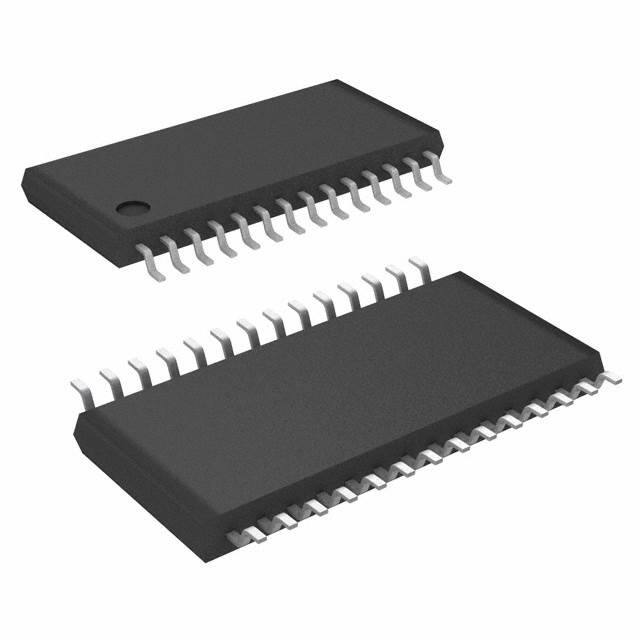
28-Lead TSSOP, 173-MIL
4.4mm x 9.7mm x 0.92mm body package
L Package
Top View
9DB206
28-Lead, 209-MIL SSOP
5.3mm x 10.2mm x 1.75mm body package
F Package
Top View
Revision B March 11, 2016
�9DB206 Data Sheet
TABLE 1. PIN DESCRIPTIONS
Number
Name
1
PLL_BW
Input
2
CLK
Input
Pulldown Non-inverting differential clock input.
3
nCLK
Input
Pullup/
Inverting differential clock input. V /2 default when left floating.
Pulldown
4
FS0
Input
5, 6
PCIEXT0,
PCIEXC0
Output
Differential output pairs. HCSL interface levels.
7, 13, 16, 22
VDD
Power
Core supply pins.
GND
Power
Power supply ground.
Output
Differential output pairs. HCSL interface levels.
Output
Differential output pairs. HCSL interface levels.
8, 21
9, 10
11, 12
14, 15
17, 18
19, 20
23, 24
Type
PCIEXT1,
PCIEXC1
PCIEXT2,
PCIEXC2
nOE0, nOE1
Input
PCIEXC3,
PCIEXT3
PCIEXC4,
PCIEXT4
PCIEXC5,
PCIEXT5
Description
Pullup
Selects PLL Bandwidth input. LVCMOS/LVTTL interface levels.
DD
Pullup
Pulldown
Frequency select pin. LVCMOS/LVTTL interface levels.
Output enable. When HIGH, forces outputs to HiZ state.
When LOW, enables outputs. LVCMOS/LVTTL interface levels.
Output
Differential output pairs. HCSL interface levels.
Output
Differential output pairs. HCSL interface levels.
Output
Differential output pairs. HCSL interface levels.
25
FS1
Input
Pulldown Frequency select pin. LVCMOS/LVTTL interface levels.
26
IREF
Input
A fixed precision resistor (475Ω) from this pin to ground provides a reference current used for differential current-mode PCIEX clock outputs.
27
GND
Power
Power supply ground.
28
VDDA
Power
Analog supply pin. Requires 24Ω series resistor.
NOTE: Pullup and Pulldown refer to internal input resistors. See Table 2, Pin Characteristics, for typical values.
TABLE 2. PIN CHARACTERISTICS
Symbol
Parameter
Test Conditions
Minimum
CIN
Input Capacitance
4
pF
RPULLUP
Input Pullup Resistor
51
kΩ
RPULLDOWN
Input Pulldown Resistor
51
kΩ
TABLE 3A. RATIO OF OUTPUT FREQUENCY TO
INPUT FREQUENCY FUNCTION TABLE, FS0
Inputs
Typical
Maximum
Units
TABLE 3B. RATIO OF OUTPUT FREQUENCY TO
INPUT FREQUENCY FUNCTION TABLE, FS1
Outputs
Inputs
Outputs
FS0
PCIEX0
PCIEX1
PCIEX2
FS1
0
1
5/4
5/4
0
1
1
1
1
1
1
1
1
5/4
5/4
5/4
TABLE 3C. OUTPUT ENABLE
FUNCTION TABLE, nOE0
TABLE 3D. OUTPUT ENABLE
FUNCTION TABLE, nOE1
PCIEX3
PCIEX5
TABLE 3E. PLL BANDWIDTH TABLE
Inputs
Outputs
Inputs
Outputs
Inputs
nOE0
PCIEX0:2
nOE1
PCIEX3:5
PLL_BW
0
Enabled
0
Enabled
0
500kHz
1
HiZ
1
HiZ
1
1MHz
©2016 Integrated Device Technology, Inc
PCIEX4
2
Bandwidth
Revision B March 11, 2016
�9DB206 Data Sheet
ABSOLUTE MAXIMUM RATINGS
Supply Voltage, VDD
4.6V
Inputs, VI
-0.5V to VDD + 0.5 V
Outputs, VO
-0.5V to VDD + 0.5V
Package Thermal Impedance, θJA
28 Lead TSSOP
28 Lead SSOP
49.8°C/W (0 lfpm)
49°C/W (0 lfpm)
Storage Temperature, TSTG
-65°C to 150°C
N OT E : S t r e s s e s b eyo n d t h o s e l i s t e d u n d e r A b s o l u t e
Maximum Ratings may cause permanent damage to the
device. These ratings are stress specifications only. Functional
operation of product at these conditions or any conditions beyond
those listed in the DC Characteristics or AC Characteristics is not
implied. Exposure to absolute maximum rating conditions for extended periods may affect product reliability.
TABLE 4A. POWER SUPPLY DC CHARACTERISTICS, VDD = VDDA = 3.3V±5%, TA = 0°C TO 70°C, RREF = 475Ω
Symbol
Parameter
Minimum
Typical
Maximum
Units
VDD
Core Supply Voltage
Test Conditions
3.135
3.3
3.465
V
VDDA
Analog Supply Voltage
3.135
3.3
3.465
V
IDD
Power Supply Current
112
mA
IDDA
Analog Supply Current
22
mA
TABLE 4B. LVCMOS / LVTTL DC CHARACTERISTICS, VDD = VDDA = 3.3V±5%, TA = 0°C TO 70°C
Symbol
Parameter
Maximum
Units
VIH
Input High Voltage
Test Conditions
2
VDD + 0.3
mV
VIL
Input Low Voltage
-0.3
0.8
mV
IIH
Input High Current
150
µA
5
µA
IIL
Input Low Current
FS1, nOE0, nOE1
Minimum
Typical
VDD = VIN = 3.465V
FS0, PLL_BW
FS1, nOE0, nOE1
VDD = 3.465V, VIN = 0V
FS0, PLL_BW
-5
µA
-150
µA
TABLE 4C. DIFFERENTIAL DC CHARACTERISTICS, VDD = VDDA = 3.3V±5%, TA = 0°C TO 70°C, RREF = 475Ω
Symbol
Parameter
Maximum
Units
IIH
Input High Current
CLK, nCLK
VDD = VIN = 3.465V
Test Conditions
Minimum
Typical
150
µA
IIL
Input Low Current
CLK, nCLK
VDD = 3.465V, VIN = 0V
150
µA
VPP
Peak-to-Peak Input Voltage
VCMR
Common Mode Input Voltage; NOTE 1, 2
0.15
1.3
V
GND + 0.5
VDD - 0.85
V
NOTE 1: Common mode voltage is defined as VIH.
NOTE 2: For single ended applications, the maximum input voltage for CLK, nCLK is VDD + 0.3V.
©2016 Integrated Device Technology, Inc
3
Revision B March 11, 2016
�9DB206 Data Sheet
TABLE 4D. HCSL DC CHARACTERISTICS, VDD = VDDA = 3.3V±5%, TA = 0°C TO 70°C, RREF = 475Ω
Symbol
Parameter
I
V
V
Output Low Voltage
I
High Impedance Leakage Current
-10
Output Crossover Voltage
250
OH
OH
OL
OZ
V
OX
Test Conditions
Minimum
Typical
Output Current
12
14
Output High Voltage
610
Maximum
Units
16
mA
780
mV
65
mV
10
µA
550
mV
Maximum
Units
140
MHz
110
ps
TABLE 5. AC CHARACTERISTICS, VDD = VDDA = 3.3V±5%, TA = 0°C TO 70°C, RREF = 475Ω
Symbol
Parameter
f
Output Frequency
tsk(o)
Output Skew; NOTE 1, 2
tjit(cc)
Cycle-to-Cycle Jitter
tjit(Ø)
RMS Phase Jitter (Random); NOTE 3
t /t
Output Rise/Fall Time
odc
Output Duty Cycle
MAX
R
F
Test Conditions
Minimum
Typical
50
Outputs @ Different Frequencies
110
ps
Outputs @ Same Frequencies
50
ps
Integration Range: 1.5MHz - 22MHz
20% to 80%
2.42
ps
300
1100
ps
48
52
%
NOTE 1: Defined as skew between outputs at the same supply voltage and with equal load conditions.
Measured at the output differential cross points.
NOTE 2: This parameter is defined in accordance with JEDEC Standard 65.
NOTE 3: Please refer to the Phase Noise Plot following this section.
©2016 Integrated Device Technology, Inc
4
Revision B March 11, 2016
�9DB206 Data Sheet
TYPICAL PHASE NOISE AT 100MHZ
➤
0
-10
-20
PCI Express™ Filter
-30
-40
100MHz
RMS Phase Jitter (Random)
1.5MHz to 22MHz = 2.42ps (typical)
-70
-80
-90
-100
Raw Phase Noise Data
-110
-120
➤
NOISE POWER dBc
Hz
-50
-60
-130
-140
-150
➤
-160
-170
-180
Phase Noise Result by adding
PCI Express™ Filter to raw data
-190
1k
10k
100k
1M
10M
100M
OFFSET FREQUENCY (HZ)
to the tracking ability of a PLL, it will track the input signal up to its
loop bandwidth. Therefore, if the input phase noise is greater than
that of the PLL, it will increase the output phase noise performance
of the device. It is recommended that the phase noise performance
of the input is verified in order to achieve the above phase noise
performance.
The illustrated phase noise plot was taken using a low phase noise
signal generator, the noise floor of the signal generator is less than
that of the device under test.
Using this configuration allows one to see the true spectral purity or
phase noise performance of the PLL in the device under test. Due
©2016 Integrated Device Technology, Inc
5
Revision B March 11, 2016
�9DB206 Data Sheet
PARAMETER MEASUREMENT INFORMATION
3.3V HCSL OUTPUT LOAD AC TEST CIRCUIT
DIFFERENTIAL INPUT LEVEL
OUTPUT SKEW
CYCLE-TO-CYCLE JITTER
OUTPUT RISE/FALL TIME
OUTPUT DUTY CYCLE/PULSE WIDTH/PERIOD
©2016 Integrated Device Technology, Inc
6
Revision B March 11, 2016
�9DB206 Data Sheet
APPLICATION INFORMATION
POWER SUPPLY FILTERING TECHNIQUES
As in any high speed analog circuitry, the power supply pins are
vulnerable to random noise. The 9DB206 provides separate power
supplies to isolate any high switching noise from the outputs to the
internal PLL. VDD and VDDA should be individually connected to the
power supply plane through vias, and bypass capacitors should be
used for each pin. To achieve optimum jitter performance, power
supply isolation is required. Figure 1 illustrates how a 24Ω resistor
along with a 10μF and a .01μF bypass capacitor should be connected to each VDDA pin. The 10Ω resistor can also be replaced by
a ferrite bead.
3.3V
VDD
.01μF
24Ω
VDDA
.01μF
10μF
FIGURE 1. POWER SUPPLY FILTERING
WIRING THE DIFFERENTIAL INPUT TO ACCEPT SINGLE ENDED LEVELS
Figure 2 shows how the differential input can be wired to accept
single ended levels. The reference voltage V_REF = VDD/2 is
generated by the bias resistors R1, R2 and C1. This bias circuit
should be located as close as possible to the input pin. The ratio
of R1 and R2 might need to be adjusted to position the V_REF in
the center of the input voltage swing. For example, if the input clock
swing is only 2.5V and VDD = 3.3V, V_REF should be 1.25V and R2/
R1 = 0.609.
FIGURE 2. SINGLE ENDED SIGNAL DRIVING DIFFERENTIAL INPUT
©2016 Integrated Device Technology, Inc
7
Revision B March 11, 2016
�9DB206 Data Sheet
DIFFERENTIAL CLOCK INPUT INTERFACE
The CLK /nCLK accepts LVDS, LVPECL, LVHSTL, SSTL, HCSL and
other differential signals. Both VSWING and VOH must meet the VPP and
VCMR input requirements. Figures 3A to 3D show interface examples
for the HiPerClockS CLK/nCLK input driven by the most common
driver types. The input interfaces suggested here are examples only.
Please consult with the vendor of the driver component to confirm
the driver termination requirements. For example in Figure 3A, the
input termination applies for ICS HiPerClockS LVHSTL drivers. If
you are using an LVHSTL driver from another vendor, use their
termination recommendation.
1.8V
3.3V
3.3V
3.3V
Zo = 50 Ohm
CLK
Zo = 50 Ohm
CLK
Zo = 50 Ohm
nCLK
Zo = 50 Ohm
nCLK
LVHSTL
ICS
HiPerClockS
LVHSTL Driver
R1
50
LVPECL
HiPerClockS
Input
R1
50
R2
50
3.3V
Zo = 50 Ohm
R2
50
R3
50
FIGURE 3A. HIPERCLOCKS CLK/NCLK INPUT DRIVEN BY
ICS HIPERCLOCKS LVHSTL DRIVER
3.3V
HiPerClockS
Input
R3
125
FIGURE 3B. HIPERCLOCKS CLK/NCLK INPUT DRIVEN BY
3.3V LVPECL DRIVER
3.3V
3.3V
3.3V
R4
125
Zo = 50 Ohm
LVDS_Driv er
CLK
CLK
R1
100
Zo = 50 Ohm
nCLK
LVPECL
R1
84
HiPerClockS
Input
Zo = 50 Ohm
nCLK
Receiv er
R2
84
FIGURE 3C. HIPERCLOCKS CLK/NCLK INPUT DRIVEN BY
3.3V LVPECL DRIVER
FIGURE 3D. HIPERCLOCKS CLK/NCLK INPUT DRIVEN BY
3.3V LVDS DRIVER
RECOMMENDATIONS FOR UNUSED INPUT AND OUTPUT PINS
INPUTS:
OUTPUTS:
LVCMOS CONTROL PINS:
All control pins have internal pull-ups or pull-downs; additional
resistance is not required but can be added for additional protection.
A 1kW resistor can be used.
©2016 Integrated Device Technology, Inc
HCSL OUTPUT
All unused HCSL outputs can be left floating. We recommend that
there is no trace attached. Both sides of the differential output pair
should either be left floating or terminated.
8
Revision B March 11, 2016
�9DB206 Data Sheet
SCHEMATIC EXAMPLE
has a slightly better signal integrity, is recommended for all other
applications.
The schematic below illustrates two different terminations. Both are
reliable and adequate. The PCI Express termination is recommended
for all PCI Express application. The optional termination, which
VCC
VCC
R11
1K
VCC
1K
33
Zo = 50
R20
1
2
3
4
5
6
7
8
9
10
11
12
13
14
FS0
33
R1
50
C11
0.1uF
U1
Zo = 50
R19
HCSL
R12
R7
VCCA
R2
50
nOE0
R13
1K
PLL_BW
CLK
nCLK
FS0
PCIEXT0
PCIEXC0
VDD
GND
PCIEXT1
PCIEXC1
PCIEXT2
PCIEXC2
VDD
nOE0
VDDA
GNDA
IREF
FS1
PCIEXT5
PCIEXC5
VDD
GND
PCIEXT4
PCIEXC4
PCIEXT3
PCIEXC3
VDD
nOE1
ICS9DB206
VCC=3.3V
28
27
26
25
24
23
22
21
20
19
18
17
16
15
FS1
24
VCC
C16
10uF
Zo = 50
+
Zo = 50
HCSL
nOE1
R10
475
R14
1K
R4
50
R15
1K
R5
50
Optional Termination
(U1-7)
VCC
C1
0.1uF
(U1-16)
C2
0.1uF
(U1-22)
C3
0.1uF
Zo = 50
R3
+
33
Zo = 50
R6
-
33
HCSL
R17
50
R18
50
PCI Express Termination
should be as close the
device as possible
PCI Express Termination
FIGURE 4. EXAMPLE OF 9DB206 SCHEMATIC
©2016 Integrated Device Technology, Inc
9
Revision B March 11, 2016
�9DB206 Data Sheet
RELIABILITY INFORMATION
TABLE 6A. θJAVS. AIR FLOW TABLE FOR 28 LEAD TSSOP PACKAGE
θJA by Velocity (Linear Feet per Minute)
0
Single-Layer PCB, JEDEC Standard Test Boards
Multi-Layer PCB, JEDEC Standard Test Boards
82.9°C/W
49.8°C/W
200
500
68.7°C/W
43.9°C/W
60.5°C/W
41.2°C/W
NOTE: Most modern PCB designs use multi-layered boards. The data in the second row pertains to most designs.
TABLE 6B. θJAVS. AIR FLOW TABLE FOR 28 LEAD SSOP PACKAGE
θJA by Velocity (Linear Feet per Minute)
Multi-Layer PCB, JEDEC Standard Test Boards
0
200
500
49°C/W
36°C/W
30°C/W
TRANSISTOR COUNT
The transistor count for 9DB206 is: 2471
©2016 Integrated Device Technology, Inc
10
Revision B March 11, 2016
�9DB206 Data Sheet
PACKAGE OUTLINE - G SUFFIX FOR 20 LEAD TSSOP
PACKAGE OUTLINE - F SUFFIX FOR 20 LEAD SSOP
TABLE 7A. PACKAGE DIMENSIONS
TABLE 7B. PACKAGE DIMENSIONS
SYMBOL
Millimeters
Millimeters
Minimum
N
Maximum
Minimum
20
N
A
--
1.20
A1
0.05
0.15
A2
0.80
1.05
b
0.19
0.30
c
0.09
0.20
D
6.40
6.60
E
E1
SYMBOL
6.40 BASIC
4.30
e
4.50
0.65 BASIC
L
0.45
α
aaa
Maximum
20
A
--
2.0
A1
0.05
--
A2
1.65
1.85
b
0.22
0.38
c
0.09
0.25
D
6.90
7.50
E
7.40
8.20
E1
5.0
5.60
0.75
e
0°
8°
L
0.55
0.95
--
0.10
α
0°
8°
Reference Document: JEDEC Publication 95, MO-153
©2016 Integrated Device Technology, Inc
0.65 BASIC
Reference Document: JEDEC Publication 95, MO-150
11
Revision B March 11, 2016
�9DB206 Data Sheet
TABLE 8. ORDERING INFORMATION
Part/Order Number
Marking
Package
Shipping Packaging
Temperature
9DB206CLLF
ICS9DB206CLLF
28 Lead “Lead-Free” TSSOP
Tube
0°C to 70°C
9DB206CLLFT
ICS9DB206CLLF
28 Lead “Lead-Free” TSSOP
Tape & Reel
0°C to 70°C
9DB206CFLF
ICS9DB206CFLF
28 Lead “Lead-Free” SSOP
Tube
0°C to 70°C
9DB206CFLFT
ICS9DB206CFLF
28 Lead “Lead-Free” SSOP
Tape & Reel
0°C to 70°C
©2016 Integrated Device Technology, Inc
12
Revision B March 11, 2016
�9DB206 Data Sheet
REVISION HISTORY SHEET
Rev
Table
Page
A
T7
12
B
T4D
B
T7
T8
1
8
12
T8
12
Features Section - added Input Frequency Range and VCO Range bullets.
Added Recommendations for Unused Input and Output Pins.
Ordering Information - removed leaded devices.
Updated data sheet format.
Ordering Information - Deleted LF note below table.
Updated header and footer.
Product Discontinuation Notice - Last time buy expires September 7, 2016.
PDN N-16-02
B
B
B
B
Description of Change
Date
Ordering Information Table - added Lead-Free marking for TSSOP package.
11/29/04
4
HCSL Table -adjusted VOH min from 680mV to 610mV and added VOH max.
12/21/04
12
Ordering Information Table - added Lead-Free marking for SSOP package.
3/21/05
1
©2016 Integrated Device Technology, Inc
13
7/14/06
7/22/15
2/18/16
3/11/16
Revision B March 11, 2016
�Part Number Data Sheet
Corporate Headquarters
6024 Silver Creek Valley Road
San Jose, CA 95138 USA
www.IDT.com
Sales
1-800-345-7015 or 408-284-8200
Fax: 408-284-2775
www.IDT.com/go/sales
Tech Support
www.idt.com/go/support
DISCLAIMER Integrated Device Technology, Inc. (IDT) reserves the right to modify the products and/or specifications described herein at any time, without notice, at IDT's sole discretion. Performance specifications and
operating parameters of the described products are determined in an independent state and are not guaranteed to perform the same way when installed in customer products. The information contained herein is provided
without representation or warranty of any kind, whether express or implied, including, but not limited to, the suitability of IDT's products for any particular purpose, an implied warranty of merchantability, or non-infringement of the intellectual property rights of others. This document is presented only as a guide and does not convey any license under intellectual property rights of IDT or any third parties.
IDT's products are not intended for use in applications involving extreme environmental conditions or in life support systems or similar devices where the failure or malfunction of an IDT product can be reasonably expected to significantly affect the health or safety of users. Anyone using an IDT product in such a manner does so at their own risk, absent an express, written agreement by IDT.
Integrated Device Technology, IDT and the IDT logo are trademarks or registered trademarks of IDT and its subsidiaries in the United States and other countries. Other trademarks used herein are the property of IDT or
their respective third party owners.
For datasheet type definitions and a glossary of common terms, visit www.idt.com/go/glossary.
Copyright ©2016 Integrated Device Technology, Inc. All rights reserved.
�IMPORTANT NOTICE AND DISCLAIMER
RENESAS ELECTRONICS CORPORATION AND ITS SUBSIDIARIES (“RENESAS”) PROVIDES TECHNICAL
SPECIFICATIONS AND RELIABILITY DATA (INCLUDING DATASHEETS), DESIGN RESOURCES (INCLUDING
REFERENCE DESIGNS), APPLICATION OR OTHER DESIGN ADVICE, WEB TOOLS, SAFETY INFORMATION, AND
OTHER RESOURCES “AS IS” AND WITH ALL FAULTS, AND DISCLAIMS ALL WARRANTIES, EXPRESS OR IMPLIED,
INCLUDING, WITHOUT LIMITATION, ANY IMPLIED WARRANTIES OF MERCHANTABILITY, FITNESS FOR A
PARTICULAR PURPOSE, OR NON-INFRINGEMENT OF THIRD PARTY INTELLECTUAL PROPERTY RIGHTS.
These resources are intended for developers skilled in the art designing with Renesas products. You are solely responsible
for (1) selecting the appropriate products for your application, (2) designing, validating, and testing your application, and (3)
ensuring your application meets applicable standards, and any other safety, security, or other requirements. These
resources are subject to change without notice. Renesas grants you permission to use these resources only for
development of an application that uses Renesas products. Other reproduction or use of these resources is strictly
prohibited. No license is granted to any other Renesas intellectual property or to any third party intellectual property.
Renesas disclaims responsibility for, and you will fully indemnify Renesas and its representatives against, any claims,
damages, costs, losses, or liabilities arising out of your use of these resources. Renesas' products are provided only subject
to Renesas' Terms and Conditions of Sale or other applicable terms agreed to in writing. No use of any Renesas resources
expands or otherwise alters any applicable warranties or warranty disclaimers for these products.
(Rev.1.0 Mar 2020)
Corporate Headquarters
Contact Information
TOYOSU FORESIA, 3-2-24 Toyosu,
Koto-ku, Tokyo 135-0061, Japan
www.renesas.com
For further information on a product, technology, the most
up-to-date version of a document, or your nearest sales
office, please visit:
www.renesas.com/contact/
Trademarks
Renesas and the Renesas logo are trademarks of Renesas
Electronics Corporation. All trademarks and registered
trademarks are the property of their respective owners.
© 2020 Renesas Electronics Corporation. All rights reserved.
�


 工商网监
湘ICP备2023018690号
工商网监
湘ICP备2023018690号
