DATASHEET
Four Output Low Power Differential Fanout Buffer for
PCI Express Gen1, Gen2, Gen3, and QPI
General Description:
9DBL411B
Features/Benefits:
The ICS9DBL411B is a 4 output lower power differential
buffer. Each output has its own OE# pin. It has a maximum
operating frequency of 150 MHz.
•
Low power differential outputs for PCIExpress and QPI clocks
•
Power down mode when all OE# are high
Recommended Application:
•
Available in I-temp
PCI-Express Gen 1/2/3 or QPI fanout buffer
•
20-pin MLF or TSSOP packaging
Output Features:
•
4 - low power differential output pairs
•
Individual OE# control of each output pair
Key Specifications:
•
Output cycle-cycle jitter < 15ps additive
•
Output to output skew: < 50ps
Power Groups
Pin Number (TSSOP)
VDD
GND
9,18
10,17
4
5
Pin Number (MLF)
VDD
GND
6,15
7,14
1
2
Description
VDD_IO for DIF(3:0)
3.3V Analog VDD & GND
Description
VDD_IO for DIF(3:0)
3.3V Analog VDD & GND
Functional Block Diagram
4
OE#(3:0)
DIF_INT
STOP
LOGIC
DIF_INC
IDT® Four Output Low Power Differential Buffer for PCI Express Gen1, Gen2, Gen3, and QPI
1
4
DIF_LPR(3:0)
1645G—09/25/18
�9DBL411B
Four Output Low Power Differential Buffer for PCI Express Gen1, Gen2, Gen3, and QPI
Advance Information
OE0#
DIF_INC
DIF_INT
VDDA
GNDA
OE3#
DIF3C_LPR
DIF3T_LPR
VDD_IO
GND
20 19 18 17 16
7
8
9 10
DIF2T_LPR
15
14
13
12
11
VDD_IO
GND
OE1#
DIF1T_LPR
DIF1C_LPR
OE2#
6
DIF2C_LPR
9DBL411B
GND
1
2
3
4
5
VDD_IO
VDDA
GNDA
OE3#
DIF3C_LPR
DIF3T_LPR
20-pin MLF
1
2
3
4
5
6
7
8
9
10
20
19
18
17
16
15
14
13
12
11
9DBL411B
DIF0C_LPR
DIF0T_LPR
OE0#
DIF_INC
DIF_INT
Pin Configurations
DIF0T_LPR
DIF0C_LPR
VDD_IO
GND
OE1#
DIF1T_LPR
DIF1C_LPR
OE2#
DIF2T_LPR
DIF2C_LPR
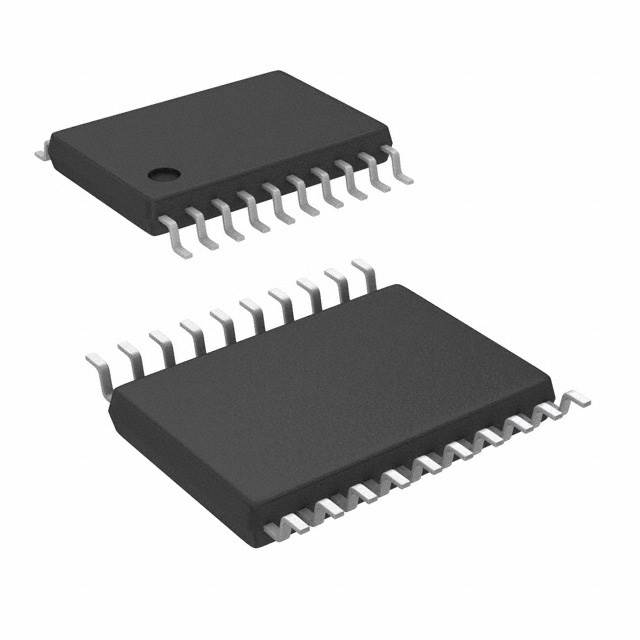
20-pin TSSOP
Terminations
Zo
9DBL411
Rs
Zo
Rs
Zo – 17 = Rs (ohms), where Zo is the single-ended intrinsic impedance of the board
transmission line. Single-ended intrinsic impedance is ½ that of the differential
impedance.
Single Ended
Rs
Impedance
5%
Rs
(Zo)
tolerance 2% tolerance
Notes
50
33
33.2
In general, 5% resistors
45
27
27.4
may be used. All values are
42.5
24 or 27
24.9
in ohms.
IDT® Four Output Low Power Differential Buffer for PCI Express for Gen1, Gen2, Gen3, and QPI
2
1645G—09/25/18
�9DBL411B
Four Output Low Power Differential Buffer for PCI Express Gen1, Gen2, Gen3, and QPI
Advance Information
TSSOP Pin Description
PIN #
(TSSOP)
PIN NAME
1
OE0#
2
3
4
5
DIF_INC
DIF_INT
VDDA
GNDA
6
OE3#
7
8
9
10
11
12
DIF3C_LPR
DIF3T_LPR
VDD_IO
GND
DIF2C_LPR
DIF2T_LPR
13
OE2#
14
15
DIF1C_LPR
DIF1T_LPR
16
OE1#
17
18
19
20
GND
VDD_IO
DIF0C_LPR
DIF0T_LPR
PIN TYPE
IN
IN
IN
PWR
GND
IN
OUT
OUT
PWR
GND
OUT
OUT
IN
OUT
OUT
IN
GND
PWR
OUT
OUT
DESCRIPTION
Output Enable for DIF0 output. Control is as follows:
0 = enabled, 1 = Low-Low
Complement side of differential input clock
True side of differential input clock
3.3V Power for the Analog Core
Ground for the Analog Core
Output Enable for DIF3 output. Control is as follows:
0 = enabled, 1 = Low-Low
Complement clock of low power differential clock pair. (no 50ohm shunt resistor to GND needed)
True clock of low power differential clock pair. (no 50ohm shunt resistor to GND needed)
Power supply for low power differential outputs, nominal 1.05V to 3.3V
Ground pin
Complement clock of low power differential clock pair. (no 50ohm shunt resistor to GND needed)
True clock of low power differential clock pair. (no 50ohm shunt resistor to GND needed)
Output Enable for DIF2 output. Control is as follows:
0 = enabled, 1 = Low-Low
Complement clock of low power differential clock pair. (no 50ohm shunt resistor to GND needed)
True clock of low power differential clock pair. (no 50ohm shunt resistor to GND needed)
Output Enable for DIF1 output. Control is as follows:
0 = enabled, 1 = Low-Low
Ground pin
Power supply for low power differential outputs, nominal 1.05V to 3.3V
Complement clock of low power differential clock pair. (no 50ohm shunt resistor to GND needed)
True clock of low power differential clock pair. (no 50ohm shunt resistor to GND needed)
IDT® Four Output Low Power Differential Buffer for PCI Express for Gen1, Gen2, Gen3, and QPI
3
1645G—09/25/18
�9DBL411B
Four Output Low Power Differential Buffer for PCI Express Gen1, Gen2, Gen3, and QPI
Advance Information
MLF Pin Description
PIN #
(MLF)
1
2
VDDA
GNDA
PWR
GND
3
OE3#
IN
4
DIF3C_LPR
OUT
5
DIF3T_LPR
OUT
6
7
VDD_IO
GND
PWR
GND
8
DIF2C_LPR
OUT
9
DIF2T_LPR
OUT
10
OE2#
11
DIF1C_LPR
OUT
12
DIF1T_LPR
OUT
13
OE1#
14
15
GND
VDD_IO
GND
PWR
16
DIF0C_LPR
OUT
17
DIF0T_LPR
OUT
18
OE0#
IN
19
20
DIF_INC
DIF_INT
IN
IN
PIN NAME
PIN TYPE
IN
IN
DESCRIPTION
3.3V Power for the Analog Core
Ground for the Analog Core
Output Enable for DIF3 output. Control is as follows:
0 = enabled, 1 = Low-Low
Complement clock of low power differential clock pair. (no 50ohm shunt resistor to
GND needed)
True clock of low power differential clock pair. (no 50ohm shunt resistor to GND
needed)
Power supply for low power differential outputs, nominal 1.05V to 3.3V
Ground pin
Complement clock of low power differential clock pair. (no 50ohm shunt resistor to
GND needed)
True clock of low power differential clock pair. (no 50ohm shunt resistor to GND
needed)
Output Enable for DIF2 output. Control is as follows:
0 = enabled, 1 = Low-Low
Complement clock of low power differential clock pair. (no 50ohm shunt resistor to
GND needed)
True clock of low power differential clock pair. (no 50ohm shunt resistor to GND
needed)
Output Enable for DIF1 output. Control is as follows:
0 = enabled, 1 = Low-Low
Ground pin
Power supply for low power differential outputs, nominal 1.05V to 3.3V
Complement clock of low power differential clock pair. (no 50ohm shunt resistor to
GND needed)
True clock of low power differential clock pair. (no 50ohm shunt resistor to GND
needed)
Output Enable for DIF0 output. Control is as follows:
0 = enabled, 1 = Low-Low
Complement side of differential input clock
True side of differential input clock
IDT® Four Output Low Power Differential Buffer for PCI Express for Gen1, Gen2, Gen3, and QPI
4
1645G—09/25/18
�9DBL411B
Four Output Low Power Differential Buffer for PCI Express Gen1, Gen2, Gen3, and QPI
Advance Information
Absolute Maximum Ratings
PARAMETER
Maximum Supply Voltage
Maximum Supply Voltage
Maximum Input Voltage
Minimum Input Voltage
Ambient Operating Temp
Storage Temperature
Input ESD protection
SYMBOL
VDDA
VDD_IO
V IH
V IL
TambCOM
TambIND
Ts
ESD prot
CONDITIONS
MIN
Core Supply Voltage
Low-Voltage Differential I/O
0.99
3.3V LVCMOS Inputs
Any Input
Vss - 0.5
0
Commercial Range
Industrial Range
-40
-65
Human Body Model
2000
MAX
4.6
3.8
4.6
70
85
150
UNITS
V
V
V
V
°C
°C
°
C
V
Notes
1,7
1,7
1,7,8
1,7
1
1
1,7
1,7
Electrical Characteristics - Input/Supply/Common Output Parameters
PARAMETER
Supply Voltage
Supply Voltage
Input High Voltage
Input Low Voltage
Differential Input High
Voltage
Differential Input Low
Voltage
Input Slew Rate - DIF_IN
Input Leakage Current
SYMBOL
VDDA
CONDITIONS
Supply Voltage
Low-Voltage Differential I/O
VDDxxx_IO
Supply
VIHSE
VILSE
VIHDIF
VILDIF
dv/dt
IIN
I DD_3.3V
Operating Supply Current
IDD_IO_133M
I DD_SB_3.3V
Power Down Current
(All OE# pins High)
Input Frequency
Pin Inductance
Input Capacitance
IDD_SBIO
Fi
Lpin
CIN
COUT
OE# latency
(at least one OE# is low)
TOE#LAT
Clock stabilization time
(from all OE# high to first
OE# low).
TSTAB
Tdrive_OE#
Tfall_OE#
Trise_OE#
TDROE#
TFALL
TRISE
MIN
3.000
MAX
3.600
UNITS
V
Notes
1
0.99
3.600
VDD +
0.3
0.8
V
1
V
V
1
1
1.15
V
1
300
mV
1
8
5
20
V/ns
uA
mA
2
1
1
20
mA
1
750
uA
1
150
150
7
5
6
uA
MHz
nH
pF
pF
1
2
1
1
1
3
periods
1
150
ns
1
10
5
5
ns
ns
ns
1
1
1
Single-ended inputs
2
Single-ended inputs
VSS - 0.3
Differential inputs
(single-ended measurement)
600
Differential inputs
(single-ended measurement) VSS - 0.3
Measured differentially
V IN = V DD , VIN = GND
VDDA supply current
VDD_IO supply @ fOP =
133MHz
VDDA supply current, Input
stopped, OE# pins all high
VDD_IO supply, Input
stopped, OE# pins all high
0.4
-5
VDD = 3.3 V
15
Logic Inputs
Output pin capacitance
1.5
Number of clocks to enable
or disable output from
assertion/deassertion of OE#
Delay from assertion of first
OE# to first clock out
(assumes input clock running
and device in power down
state))
Output enable after
OE# de-assertion
1
Fall/rise time of OE# inputs
IDT® Four Output Low Power Differential Buffer for PCI Express for Gen1, Gen2, Gen3, and QPI
5
1645G—09/25/18
�9DBL411B
Four Output Low Power Differential Buffer for PCI Express Gen1, Gen2, Gen3, and QPI
Advance Information
AC Electrical Characteristics - DIF Low Power Differential Outputs
PARAMETER
Rising Edge Slew Rate
Falling Edge Slew Rate
Slew Rate Variation
Maximum Output Voltage
Minimum Output Voltage
Differential Voltage Swing
Crossing Point Voltage
Crossing Point Variation
SYMBOL
tSLR
tFLR
tSLVAR
VHIGH
VLOW
VSWING
VXABS
VXABSVAR
Duty Cycle Distortion
DCYCDIS0
Additive Cycle to Cycle
Jitter
DIF[3:0] Skew
Propagation Delay
Additive Phase Jitter PCIe Gen1
DIFJ C2CADD
DIFSKEW
tPD
tphase_add
CONDITIONS
Differential Measurement
Differential Measurement
Single-ended Measurement
Includes overshoot
Includes undershoot
Differential Measurement
Single-ended Measurement
Single-ended Measurement
Differential Measurement,
fIN


 工商网监
湘ICP备2023018690号
工商网监
湘ICP备2023018690号

