DATASHEET
Low Power Clock for Intel Atom®-Based Systems
9LPRS436C
Key Specifications:
•
CPU outputs cycle-cycle jitter < 85ps
•
PCIEX outputs cycle-cycle jitter < 125ps
•
SATA outputs cycle-cycle jitter < 125ps
•
PCI outputs cycle-cycle jitter < 500ps
•
+/- 100ppm frequency accuracy on all clocks
Recommended Application:
NM10 Express Chipset + N450/D410/D510 Atom® CPUs
Output Features:
•
2 - 0.8V push-pull differential CPU pairs
•
2 - 0.8V push-pull differential PCIEX pairs
•
1 - 0.8V push-pull differential SATA75 pair
•
1 - 0.8V push-pull differential DOT96 pair
•
1 - 0.8V push-pull differential CPU/PCIEX selectable pair
•
1 - PCI (33MHz)
•
1 - PCICLK_F, (33MHz) free-running
•
1 - USB, 48MHz
•
1 - 12/48MHz
•
1 - 25MHz
•
1 - REF, 14.318MHz
•
1 - 12.288MHz
Features/Benefits:
•
VDDSUSP allows 25MHz to run in S-states
•
Supports programmable spread percentage
•
Uses external 25MHz crystal, external crystal load caps
are required for frequency tuning
•
PEREQ# pins to support PCIEX/SATA power
management.
•
Low power differential clock outputs (No 50Ω resistor to
GND needed)
•
Integrated 33Ω series resistor on all differential outputs.
**FS3/12_288M_2x
VDD12_288
PEREQ1#
PEREQ2#
**FS4/PCICLK0_2x
GND
VDDPCI
**ITP_EN/PCICLK_F0_2x
PEREQ3#
*SEL12_48#/12_48MHz_2x
VDD
FSLA/USB48_2x
GND
DOTT_96MHzLR
DOTC_96MHzLR
FSLB
GNDSATA
SATAT_LR/PCIeT_LR3
SATAC_LR/PCIeC_LR3
VDDSATA
PCIeT_LR0
PCIeC_LR0
PCIeT_LR1
PCIeC_LR1
1
2
3
4
5
6
7
8
9
10
11
12
13
14
15
16
9LPRS436
Pin Configuration
17
18
19
20
21
22
23
24
48
47
46
45
44
43
42
41
40
39
38
37
36
35
34
33
32
31
30
29
28
27
26
25
GND
GND
REF0_2x/FSLC
VDD14
Vtt_PwrGd/WOL_STOP#
VDDSUSP
25MHz
GND
X1_25
X2_25
PCI&PCIEX_STOP#
CPU_STOP#
SDATA
SCLK
GND
CPUT_LR0
CPUC_LR0
VDDCPU
CPUT_LR1
CPUC_LR1
CPUITPT_LR2/PCIeT_LR2
CPUITPC_LR2/PCIeC_LR2
VDDPCIEX
GND
48-TSSOP
* Internal Pull-Up Resistor
** Internal Pull-Down Resistor
IDT® Low Power Clock for Intel Atom®-Based Systems
1561C —08/24/11
1
�CPU_STOP#
PCI&PCIEX_STOP#
X2_25
X1_25
GND
25MHz
VDDSUSP
Vtt_PwrGd/WOL_STOP#
VDD14
REF0_2x/FSLC
GND
GND
9LPRS436C
Low Power Clock for Intel Atom ® -Based Systems
48 47 46 45 44 43 42 41 40 39 38 37
**FS3/12_288M_2x 1
36 SDATA
VDD12_288 2
35 SCLK
PEREQ1# 3
34 GND
PEREQ2# 4
33 CPUT_LR0
9LPRS436
**FS4/PCICLK0_2x 5
32 CPUC_LR0
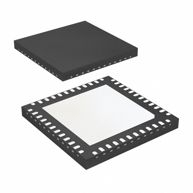
48 MLF
6x6mm
0.4mm pitch
GND 6
VDDPCI 7
**ITP_EN/PCICLK_F0_2x 8
PEREQ3# 9
31 VDDCPU
30 CPUT_LR1
29 CPUC_LR1
28 CPUITPT_LR2/PCIeT_LR2
*SEL12_48#/12_48MHz_2x 10
27 CPUITPC_LR2/PCIeC_LR2
VDD 11
FSLA/USB48_2x 12
26 VDDPCIEX
25 GND
PCIeC_LR1
PCIeT_LR1
PCIeC_LR0
PCIeT_LR0
VDDSATA
SATAC_LR/PCIeC_LR3
SATAT_LR/PCIeT_LR3
GNDSATA
FSLB
DOTC_96MHzLR
DOTT_96MHzLR
GND
13 14 15 16 17 18 19 20 21 22 23 24
* Internal Pull-Up Resistor
** Internal Pull-Down Resistor
IDT® Low Power Clock for Intel Atom®-Based Systems
1561C — 08/24/11
2
�9LPRS436C
Low Power Clock for Intel Atom ® -Based Systems
Pin Description
PIN #
PIN NAME
1
**FS3/12_288M_2x
2
VDD12_288
3
PEREQ1#
4
PEREQ2#
5
6
7
**FS4/PCICLK0_2x
GND
VDDPCI
8
**ITP_EN/PCICLK_F0_2x
9
PEREQ3#
10
*SEL12_48#/12_48MHz_2x
11
VDD
12
FSLA/USB48_2x
13
GND
14
DOTT_96MHzLR
15
DOTC_96MHzLR
16
FSLB
17
GNDSATA
18
SATAT_LR/PCIeT_LR3
19
SATAC_LR/PCIeC_LR3
20
VDDSATA
21
PCIeT_LR0
22
PCIeC_LR0
23
PCIeT_LR1
24
PCIeC_LR1
TYPE
DESCRIPTION
I/O
Frequency select latch input pin / 12.288MHz output, 3.3V
PWR Power for 12.288MHz PLL and output buffer, nominal 3.3V.
Real-time input pin that controls SATACLK and PCIEXCLK outputs that are
IN
selected through the SMBus. 1 = selected outputs are disabled, 0 = selected
outputs are enabled.
Real-time input pin that controls SATACLK and PCIEXCLK outputs that are
IN
selected through the SMBus. 1 = selected outputs are disabled, 0 = selected
outputs are enabled.
I/O
Frequency select latch input pin / 3.3V PCI clock output.
PWR Ground pin.
PWR Power supply for PCI clocks, nominal 3.3V
ITP Enable Latched Input/Free Running PCI clock output.
ITP_Enable Selects the functionality of the CPU_ITP/SRC output as follows:
I/O
1 = CPU_ITP output
0 = SRC output
Real-time input pin that controls PCIEXCLK outputs that are selected through
IN
the SMBus. 1 = selected outputs are disabled, 0 = selected outputs are
enabled.
Latched select input for 12/48MHz output. 1=12MHz, 0=48MHz. 12/48MHz
I/O
clock output.
PWR Power supply, nominal 3.3V
3.3V tolerant input for CPU frequency selection. Low voltage threshold inputs,
I/O
see input electrical characteristics for Vil_FS and Vih_FS values. / 48.00MHz
USB clock
PWR Ground pin.
True clock of low power differential pair for 96.00MHz DOT clock. No 50ohm
OUT
to GND needed. No Rs needed.
Complementary clock of low power differential pair for 96.00MHz DOT clock.
OUT
No 50ohm resistor to GND needed. No Rs needed.
3.3V tolerant input for CPU frequency selection. Refer to input electrical
IN
characteristics for Vil_FS and Vih_FS values.
PWR Ground pin for the SATA outputs
True clock of differential SATA pair. / True clock of differential PCI-Express pair
OUT - selectable by FS(4:3) ; both are 0.8V differential push pull outputs with
integrated 33ohm series resistor.
Complementary clock of differential SATA pair. / Complementary clock of
OUT differential PCI-Express pair - selectable by FS(4:3); both are 0.8V differential
push pull outputs with integrated 33ohm series resistor.
PWR Supply for SATA clocks, 3.3V nominal
True clock of 0.8V differential push-pull PCI_Express pair with integrated
OUT
33ohm series resistor
Complementary clock of 0.8V differential push-pull PCI_Express pair with
OUT
integrated 33ohm series resistor
True clock of 0.8V differential push-pull PCI_Express pair with integrated
OUT
33ohm series resistor
Complementary clock of 0.8V differential push-pull PCI_Express pair with
OUT
integrated 33ohm series resistor
IDT® Low Power Clock for Intel Atom®-Based Systems
1561C — 08/24/11
3
�9LPRS436C
Low Power Clock for Intel Atom ® -Based Systems
Pin Description (Continued)
25
26
GND
VDDPCIEX
PWR
PWR
27
CPUITPC_LR2/PCIeC_LR2
OUT
28
CPUITPT_LR2/PCIeT_LR2
OUT
29
CPUC_LR1
OUT
30
CPUT_LR1
OUT
31
VDDCPU
PWR
32
CPUC_LR0
OUT
33
CPUT_LR0
OUT
34
35
36
37
GND
SCLK
SDATA
CPU_STOP#
PWR
IN
I/O
IN
38
PCI&PCIEX_STOP#
39
40
41
42
X2_25
X1_25
GND
25MHz
OUT
IN
PWR
OUT
43
VDDSUSP
PWR
44
Vtt_PwrGd/WOL_STOP#
45
VDD14
46
REF0_2x/FSLC
47
48
GND
GND
IN
IN
PWR
I/O
PWR
PWR
Ground pin.
Power supply for PCI Express clocks, nominal 3.3V
Complementary clock of differential pair CPU output. / Complementary clock of
differential PCIEX pair. These are 0.8V push pull outputs. No external 50ohm
resistor to GND or 33ohm series resistor needed.
True clock of differential pair CPU output. / True clock of differential PCIEX
pair. These are 0.8V push pull outputs. No external 50ohm resistor to GND or
33ohm series resistor needed.
Complementary clock of differential pair 0.8V push-pull CPU outputs with
integrated 33ohm series resistor.
True clock of differential pair 0.8V push-pull CPU outputs with integrated
33ohm series resistor.
Supply for CPU clocks, 3.3V nominal
Complementary clock of differential pair 0.8V push-pull CPU outputs with
integrated 33ohm series resistor.
True clock of differential pair 0.8V push-pull CPU outputs with integrated
33ohm series resistor.
Ground pin.
Clock pin of SMBus circuitry, 5V tolerant.
Data pin for SMBus circuitry, 5V tolerant.
Stops CPU0 clock when enabled.
Stops all PCICLKs at logic 0 level, when low. Free running PCICLKs are not
effected by this input.
Crystal output, Nominally 25.00MHz.
Crystal input, Nominally 25.00MHz.
Ground pin.
25MHz clock output, 3.3V
Supply for suspend mode, powers 25MHz PLL, 25M output and XTAL
oscillator. 3.3V Nominal
This active high 3.3V LVTTL input is a level sensitive strobe used to determine
when latch inputs are valid and are ready to be sampled / Asynchronous active
low input pin that stops all outputs except free running 25Mhz
Power for 14.31818MHz PLL and REF output, nominal 3.3V.
2x strength 14.318 MHz reference clock./ 3.3V tolerant input for CPU frequency
selection. Refer to input electrical characteristics for Vil_FS and Vih_FS
values.
Ground pin.
Ground pin.
IDT® Low Power Clock for Intel Atom®-Based Systems
1561C — 08/24/11
4
�9LPRS436C
Low Power Clock for Intel Atom ® -Based Systems
General Description
The 9LPRS436C is a low power CK505-compatible clock targeted at Intel-based Netbooks and Nettops. This clock synthesizer
provides a single chip solution for systems using the Intel NM10 chipset paired with the Intel N450/D410/D510 Atom® CPUs. The
9LPRS436C is driven with a 25MHz crystal.
25M
Block Diagram
NonSS
PLL
14.318M
NonSS
PLL
12.288M
CPU
25M
XTAL
PCI
SS PLL
PCIe/
SATA
75M/
100M
NonSS
PLL
DOT96
48MHz
12_48MHz
Series Resistors for Single Ended Outputs
D.C.Drive Strength
Number of
Loads
to Drive
Match Point for N & P
Voltage / Current (mA)
1
2
Number of Loads Actually Driven.
1 Load
Rs=
2 Loads
Rs=
3 Loads
Rs=
0.56 / 33 (17Ω)
33Ω [39Ω]
-
-
0.92 / 66 (14Ω)
39Ω [43Ω]
22Ω [27Ω]
-
Notes:
1. Preferred drive strengths using CK505 clock sources. Transmission lines to load do not share
series resistors.
2. Desktop/Mobile Platforms with Zo = 50/55 ohms use the first resistor value.
3. Systems with Zo = 60 ohms use the resistor values in brackets [ ].
IDT® Low Power Clock for Intel Atom®-Based Systems
1561C — 08/24/11
5
�9LPRS436C
Low Power Clock for Intel Atom ® -Based Systems
Table 1: CPU/SRC/PCI PLL Spread Frequency Selection Table for 9LPRS436C
0
1
2
3
4
5
6
7
8
9
10
11
12
13
14
15
16
17
18
19
20
21
22
23
24
25
26
27
28
29
30
31
FS4
(B0b4)
FS3
(B0b3)
FSLC
(B0b2)
0
0
0
0
0
0
0
0
0
0
0
0
0
0
0
0
1
1
1
1
1
1
1
1
1
1
1
1
1
1
1
1
0
0
0
0
0
0
0
0
1
1
1
1
1
1
1
1
0
0
0
0
0
0
0
0
1
1
1
1
1
1
1
1
0
0
0
0
1
1
1
1
0
0
0
0
1
1
1
1
0
0
0
0
1
1
1
1
0
0
0
0
1
1
1
1
FSLB FSLA
(B0b1) (B0b0)
0
0
1
1
0
0
1
1
0
0
1
1
0
0
1
1
0
0
1
1
0
0
1
1
0
0
1
1
0
0
1
1
0
1
0
1
0
1
0
1
0
1
0
1
0
1
0
1
0
1
0
1
0
1
0
1
0
1
0
1
0
1
0
1
IDT® Low Power Clock for Intel Atom®-Based Systems
CPU
MHz
SRC
PCI
SATA
100.00
100.00
83.33
83.33
133.33
133.33
166.67
166.67
100.00
100.00
83.33
83.33
133.33
133.33
166.67
166.67
100.00
100.00
83.33
83.33
133.33
133.33
166.67
166.67
100.00
100.00
83.33
83.33
133.33
133.33
166.67
166.67
100.00
100.00
100.00
100.00
100.00
100.00
100.00
100.00
100.00
100.00
100.00
100.00
100.00
100.00
100.00
100.00
100.00
100.00
100.00
100.00
100.00
100.00
100.00
100.00
100.00
100.00
100.00
100.00
100.00
100.00
100.00
100.00
33.33
33.33
33.33
33.33
33.33
33.33
33.33
33.33
33.33
33.33
33.33
33.33
33.33
33.33
33.33
33.33
33.33
33.33
33.33
33.33
33.33
33.33
33.33
33.33
33.33
33.33
33.33
33.33
33.33
33.33
33.33
33.33
Follows SRC
Follows SRC
Follows SRC
Follows SRC
Follows SRC
Follows SRC
Follows SRC
Follows SRC
100MHz Non-Spread
100MHz Non-Spread
100MHz Non-Spread
100MHz Non-Spread
100MHz Non-Spread
100MHz Non-Spread
100MHz Non-Spread
100MHz Non-Spread
75MHz Non-Spread
75MHz Non-Spread
75MHz Non-Spread
75MHz Non-Spread
75MHz Non-Spread
75MHz Non-Spread
75MHz Non-Spread
75MHz Non-Spread
75MHz Non-Spread
75MHz Non-Spread
75MHz Non-Spread
75MHz Non-Spread
75MHz Non-Spread
75MHz Non-Spread
75MHz Non-Spread
75MHz Non-Spread
1561C — 08/24/11
6
�9LPRS436C
Low Power Clock for Intel Atom ® -Based Systems
Table 2: Slew Rate Selection Table
Slew
Bit 1
Bit 0
Rate
Hi-Z
0
0
0.6X
0
1
(1.2V/ns)
0.8X
1
0
(1.6V/ns)
1X
1
1
(2.0V/ns)
CPU Power Management Table
WOL_STOP#
SMBus
Register OE
PCI&PCIEX_
CPU(1:0)/ITP CPU#(1:0)/ITP
STOP#
CPU_STOP#
1
Enable
1
X
Running
1
Enable
0
X
High
Running
Low
0
Enable
X
X
Low
Low
X
Disable
X
X
Low
Low
Differential Power Management Table
PCI&PCIEX_ PCIEX/SATA PCIEX/SATA# PCIEX/SATA PCIEX/SATA#
STOP#
PCI Stoppable
Free-Run
WOL_STOP#
SMBus
Register OE
CPU_STOP#
1
Enable
X
1
Enable
X
0
High
0
Enable
X
X
Low
X
Disable
X
X
Low
Low
PCI&PCIEX_
STOP#
PCIF/PCI
PCIF/PCI
Free-run
Stoppable
1
Running
Running
DOT
DOT#
Running
Running
Running
Running
Low
Running
Running
Running
Running
Low
Low /20K
Low
Low /20K
Low
Low /20K
Low
Low /20K
Low
REF
12/48MHz
12.288MHz
25MHz
25MHz
Singled-ended Power Management Table
WOL_STOP#
SMBus
Register OE
CPU_STOP#
Free-run Stoppable
1
Enable
X
1
Running
Running
Running
Running
Running
Running
1
Enable
X
0
Running
Low
Running
Running
Running
Running
0
Enable
X
X
Low
Low
Low
Low
Running
Low
X
Disable
X
X
Low
Low
Low
Low
Low
Low
PEREQ# Control Table:
PEREQ#
PCIe
controlled
1
0, SATA/PCIe3
2
SATA/PCIe3, 1
3
1, 2
IDT® Low Power Clock for Intel Atom®-Based Systems
1561C — 08/24/11
7
�9LPRS436C
Low Power Clock for Intel Atom ® -Based Systems
Electrical Characteristics - Absolute Maximum Ratings
PARAMETER
3.3V Core Supply Voltage
3.3V Logic Supply Voltage
Input Low Voltage
Input High Voltage
Input High Voltage
Storage Temperature
Case Temperature
Input ESD protection
SYMBOL
VDDA
VDD
VIL
V IH
V IHSMB
Ts
Tcase
ESD prot
CONDITIONS
MIN
TYP
UNITS NOTES
V
1,2
V
1,2
V
1
V DD +0.5V
V
1
5.5V
V
1
°
150
C
1
115
°C
1
V
1
TYP
MAX
85
85
3.465
V DD + 0.3
0.8
UNITS
°C
°C
V
V
V
VDD + 0.3
V
GND-0.5
Except for SMBus interface
SMBus clock and data pins
-65
Human Body Model
2000
MAX
4.6
4.6
1
Guaranteed by design and characterization, not 100% tested in production.
2
Operation under these conditions is neither implied nor guaranteed.
Electrical Characteristics - Input/Supply/Common Output DC Parameters
PARAMETER
Supply Voltage
Input High Voltage
Input Low Voltage
Tam bI
VDDxxx
VI HSE
VILSE
CONDITIONS
Standard Device
Industrial Temperature R ange Device
Supply Voltage
Single-ended 3.3V inputs
Single-ended 3.3V inputs
FS(4:3) Input High Voltage
V IH_FS4
Single-ended 3.3V FS(4:3) Inputs
2
FS(4:3) Input Low Voltage
Low Threshold InputHigh Voltage
Low Threshold InputLow Voltage
Input Leakage Current
VIL_ FS4
Single-ended 3.3V FS(4:3) Inputs
VSS - 0.3
0.8
V
V IH_FS
3.3 V +/-5%
0.7
VDD+0.3
V
VIL _FS
3.3 V +/-5%
VSS - 0.3
0.35
V
IIN
-5
5
uA
Input Leakage Current
IINRES
-200
200
uA
Output High Voltage
Output Low Voltage
V OHSE
VOLSE
VIN = V DD , VIN = GND
Inputs with pull up or pull down resistors
VIN = V DD , VIN = GND
Single-ended outputs, IOH = -1mA
Single-ended outputs, IOL = 1 mA
Full Active, CL = Full load; IDD 3.3V
Full Active, CL = Full load; IDD 3.3V
3.3V Main Rail
VDD_SUSP Rail. 25MHz Running (WOL)
VDD_SUSP Rail. 25MHz Off
V DD = 3.3 V
0.4
115
15
0
15
4
27
7
5
6
6
5.5
0.4
V
V
mA
mA
mA
mA
mA
MHz
nH
pF
pF
pF
V
V
Ambient Operating Temp
Operating Supply Current
Powerdown Current
Input Frequency
Pin Inductance
Input Capacitance
SMBus Voltage
Low-level Output Voltage
Current sinking at
VOLSM B = 0.4 V
SCLK/SDATA
Clock/Data Rise Time
SCLK/SDATA
Clock/D ata Fall Time
Maximum SMBus Operating Frequency
Spread Spectrum Modulation Frequency
SYMBOL
T amb C
I DDVD D3.3
ID DVD DSUSP3 .3
ID DPD VDD3 .3
ID DPD SUSP3.3w
IDD PDSU SP3.3
Fi
L pin
CIN
COUT
CIN X
V DD
VOLSMB
Logic Inputs
Output pin capacitance
X1 & X2 pins
TF I2C
FSMBUS
fSSM OD
2.4
106
12
12
3
1.5
2.7
@ IPUL LUP
I PULLU P
TR I2C
MIN
0
-40
3.135
2
VSS - 0.3
SMB Data Pin
4
30
7
7
6
5
5
8
mA
(Max VIL - 0.15) to
(Min VIH + 0.15)
(Min VIH + 0.15) to
(Max VIL - 0.15)
Triangular Modulation
Notes
32.5
1000
ns
300
ns
100
33
kH z
kH z
NOTES on DC Parameters: (unless otherwise noted, guaranteed by design and characterization, not 100% tested in production).
1
2
Operation at these points is not recommended
Maximum VIH is not to exceed VDD
3
Human Body Model
Operation under these conditions is nei ther implied, nor guaranteed.
S ignal is required to be monotonic in this region.
4
5
6
7
8
Input leakage current does not include inputs with pull-up or pull-down resistors
3.3V referenced inputs are: PCI&P CIEX_STOP #, CPU_STOP #, ITP_EN, SCLK, SDATA, VTT_PWR_GD/P D#, SEL12_48# and PEREQ# inputs if selected.
For margining purposes only. Normal operation should have Fin = 25MHz +/-50ppm
IDT® Low Power Clock for Intel Atom®-Based Systems
1561C — 08/24/11
8
�9LPRS436C
Low Power Clock for Intel Atom ® -Based Systems
AC Electrical Characteristics - Input/Common Parameters
PARAMETER
SYMBOL
Clk Stabilization
T STAB
Tdrive_PEREQ_off
Tdrive_PEREQ_on
TD RPER OFF
TD RPERON
Tdrive_CPU
TDRSR C
Tdrive_PCIEX
TD RPC IEX
Tfall_SE
Trise_SE
TFALL
TR ISE
Tdrive_PD#
TD RPD
CONDITIONS
From VDD Power-Up or de-assertion of PD to
1st clock
Output stop after PEREQ# deasserted
Output run after PEREQ# asserted
CPU output enable after
CPU_STOP# de-assertion
PCIEX output enable after
PCI&PCIEX_STOP# de-assertion
Fall/rise time of all 3.3V control inputs from 2080%
Differential output enable after
PD# de-assertion
MIN
TYP
MAX
UNITS
1.1
1.8
ms
2
2
3
3
clocks
clocks
8
10
ns
8
15
ns
10
10
ns
ns
85
300
us
TYP
3.3
3.2
16
806
MAX
4
4
20
1150
395
32
49.7
66
125
66
66
65
38
145
44
550
140
55
85
150
125
125
250
100
150
250
Notes
1
1
AC Electrical Characteristics - CPU, PCIEX, SATA, DOT96MHz
PARAMETER
Rising Edge Slew Rate
Falling Edge Slew Rate
Slew Rate Variation
Maximum Output Voltage
Minimum Output Voltage
Differential Voltage Swing
Crossing Point Voltage
Crossing Point Variation
Duty Cycle
CPU Jitter - Cycle to Cycle
CPU2_IPT Jitter - Cycle to Cycle
SRC Jitter - Cycle to Cycle
SATA Jitter - Cycle to C ycle
DOT Jitter - Cycle to Cycle
CPU[1:0] Skew
CPU[2_ITP:0] Skew
SRC Skew
SYMBOL
tSLR
tFLR
tSLVAR
VHIGH
VLOW
VSWING
VXABS
VXABSVAR
DCYC
CPUJC2C
CPU2JC2C
SRCJC2C
SATAJC2C
DOTJC2C
CPUSKEW10
CPUSKEW20
SRCSKEW
CONDITIONS
Differential Measurement
Differential Measurement
Single-ended Measurement
Includes overshoot
Includes undershoot
Differential Measurement
Single-ended Measurement
Single-ended Measurement
Differential Measurement
Differential Measurement
Differential Measurement
Differential Measurement
Differential Measurement
Differential Measurement
Differential Measurement
Differential Measurement
Differential Measurement
MIN
2.5
2.5
-300
300
300
45
UNITS NOTES
V/ns
1,2
V/ns
1,2
%
1
mV
1
mV
1
mV
1
mV
1,3,4
mV
1,3,5
%
1
ps
1
ps
1
ps
1
ps
1
ps
1
ps
1,6
ps
1,6
ps
1
Electrical Characteristics - PCICLK/PCICLK_F
PARAMETER
Output Impedance
Long Accuracy
SYMBOL
RDSP
ppm
Clock period
T period
Absolute min/max period
Tabs
Output High Voltage
Output Low Voltage
V OH
VOL
Output High Current
IOH
Output Low Current
IOL
Rising Edge Slew Rate
Falling Edge Slew Rate
Duty Cycle
Pin to Pin Skew
Jitter, Cycle to cycle
tSLR
tFLR
d t1
t skew
tjcyc-cyc
CON DITIONS
VO = VD D*(0.5)
see Tperiod min-max values
33.33MHz output no spread
33.33MHz output spread
33.33MHz output no spread
33.33MHz output nominal/spread
IOH = -1 mA
IOL = 1 mA
V OH @MIN = 1.0 V
VOH @MAX = 3.135 V
VOL @ MIN = 1.95 V
VOL @ MAX = 0.4 V
Measured from 0.8 to 2.0 V
Measured from 2.0 to 0.8 V
V T = 1.5 V
V T = 1.5 V
V T = 1.5 V
MIN
12
-100
29.99700
30.08421
29.49700
29.56617
2.4
TYP
-33
30
1
1
45
1.7
1.8
50.6
150
MAX
UNITS NOTES
Ω
55
1
100
ppm
2
30.00300
ns
2
30.23459
ns
2
30.50300
ns
2
30.58421
ns
2
V
1
0.4
V
1
mA
1
-33
mA
1
mA
1
38
mA
1
4
V/ns
1
4
V/ns
1
55
%
1
250
ps
1
500
ps
1
*T A = Tambient; VDD = 3.3 V +/-5%; C L=5pF, Rs=22Ω (unless specified otherwise)
1
Guaranteed by design and characterization, not 100% tested in p rod uction.
2
All Long Term Accuracy and Clock Period specifications are guaranteed assuming that REFOUT is at 14.31818MHz
3
Slew rate emastured through V_swing voltage range cente red about differential zero
4
Vcross is defined at the voltage where Clock = Clock#.
5
Only appli es to the differential rising edge (Clock rising, Clock# falling.)
6
CPU group skew is nominally 0ps.
IDT® Low Power Clock for Intel Atom®-Based Systems
1561C — 08/24/11
9
�9LPRS436C
Low Power Clock for Intel Atom ® -Based Systems
Electrical Characteristics - USB48MHz, 12/48MHz
PARAMETER
Long Accuracy
Clock period
Absolute min/max period
Output High Voltage
Output Low Voltage
Rising Edge Slew Rate (USB48M)
Falling Edge Slew Rate (USB48M)
Rising Edge Slew Rate (12/48M)
Falling Edge Slew Rate (12/48M)
Duty Cycle
Jitter, Cycle to cycle
SYMBOL
ppm
T period
Tabs
V OH
VOL
tSLR
tFLR
tSLR
tFLR
d t1
tjcyc-cyc
CON DITIONS
see Tperiod min-max values
48.00MHz output nominal
48.00MHz output nominal
IOH = -1 mA
IOL = 1 mA
Measured from 0.8 to 2.0 V
Measured from 2.0 to 0.8 V
Measured from 0.8 to 2.0 V
Measured from 2.0 to 0.8 V
V T = 1.5 V
V T = 1.5 V
MIN
-100
20.83125
20.48125
2.4
TYP
MAX
UNITS NOTES
100
ppm
1,2
20.83542
ns
2,3
21.18542
ns
2
V
1
0.4
V
1
2
V/ns
1
2
V/ns
1
2
V/ns
1
2
V/ns
1
55
%
1
350
ps
1
1
1
1
1
45
1.7
1.7
1.7
1.7
50.6
150
SYMBOL
ppm
T period
Tabs
V OH
VOL
tSLR
tFLR
d t1
tjcyc-cyc
CON DITIONS
see Tperiod min-max values
25.00MHz output nominal
25.00MHz output nominal
IOH = -1 mA
IOL = 1 mA
Measured from 0.8 to 2.0 V
Measured from 2.0 to 0.8 V
V T = 1.5 V
V T = 1.5 V
MIN
-100
39.99600
39.32360
2.4
TYP
0
1
1
45
1.8
1.8
49.6
150
SYMBOL
ppm
T period
Tabs
V OH
VOL
tSLR
tFLR
d t1
tjcyc-cyc
CON DITIONS
see Tperiod min-max values
12.288MHz output nominal
12.288MHz output nominal
IOH = -1 mA
IOL = 1 mA
Measured from 0.8 to 2.0 V
Measured from 2.0 to 0.8 V
V T = 1.5 V
V T = 1.5 V
MIN
-100
81.37207
80.87207
2.4
TYP
0
1
1
45
1.8
1.8
50.1
133
CONDITIONS
see Tperiod min-max values
14.318MHz output nominal
14.318MHz output nominal
IOH = -1 mA
IOL = 1 mA
Measured from 0.8 to 2.0 V
Measured from 2.0 to 0.8 V
VT = 1.5 V
VT = 1.5 V
MIN
-100
69.82033
69.83400
2.4
TYP
0
1
1
45
1.5
1.4
50.2
139
0.4
4
4
55
1000
MIN
TYP.
30
MAX
86
1.3
3
1.7
3.1
Electrical Characteristics - 25MHz
PARAMETER
Long Accuracy
Clock period
Absolute min/max period
Output High Voltage
Output Low Voltage
Rising Edge Slew Rate
Falling Edge Slew Rate
Duty Cycle
Jitter, Cycle to cycle
MAX
UNITS NOTES
100
ppm
1,2
40.00400
ns
2,3
40.67640
ns
2
V
1
0.4
V
1
2
V/ns
1
2
V/ns
1
55
%
1
500
ps
1
Electrical Characteristics - 12.288MHz
PARAMETER
Long Accuracy
Clock period
Absolute min/max period
Output High Voltage
Output Low Voltage
Rising Edge Slew Rate
Falling Edge Slew Rate
Duty Cycle
Jitter, Cycle to cycle
MAX
100
81.38835
81.88835
0.4
2
2
55
500
UNITS NOTES
ppm
1,2
ns
2,3
ns
2
V
1
V
1
V/ns
1
V/ns
1
%
1
ps
1
Electrical Characteristics - REF-14.318MHz
PARAMETER
Long Accuracy
Clock period
Absolute min/max period
Output High Voltage
Output Low Voltage
Rising Edge Slew Rate
Falling Edge Slew Rate
Duty Cycle
Jitter, Cycle to cycle
SYMBOL
ppm
Tperiod
Tabs
VOH
VOL
tSLR
tFLR
dt1
tjcyc-cyc
MAX
100
69.86224
70.84800
UNITS
ppm
ns
ns
V
V
V/ns
V/ns
%
ps
Notes
1,2
2,3
2
1
1
1
1
1
1
*T A = Tambient; VDD = 3.3 V +/-5%; C L=5pF, Rs=22Ω (unless specified otherwise)
1
Guaranteed by design and characterization, not 100% tested in p rod uction.
2
All Long Term Accuracy and Clock Period specifications are guaranteed assuming that REFOUT is at 14.31818MHz
3
The average period over any 1us period of time
Electrical Characteristics - Phase Jitter
PARAMETER
SYMBOL
tjp hPCIe1
Jitter, Phase
tjph PCIe2L o
tjphPC Ie2Hi
CONDITIONS
PCIe Gen 1 REFCLK phase jitter
PCIe Gen 2 REFCLK phase jitter
Lo-band content
PCIe Gen 2 REFCLK phase jitter
Hi-band content
UNITS NOTES
ps
1,2,3
ps
1,2,3
(RMS)
ps
1,2,3
(RMS)
*T A = Tambient; VDD = 3.3 V +/-5%; C L=5pF, Rs=22Ω (unless specified otherwise)
Notes on Phase Jitter:
1
See http://www.pcisig.com for complete specs. Guaranteed by design and characterization, not tested in production.
Device driven by 932S421BGLF or equivalent
-12
Sample size of at least 100K cycles. This figures extrapolates to 108ps pk-pk @ 1M cycles for a B ER of 1
3
Applies to PCIEX(3:0) outputs only.
2
2
IDT® Low Power Clock for Intel Atom®-Based Systems
1561C — 08/24/11
10
�9LPRS436C
Low Power Clock for Intel Atom ® -Based Systems
Driving LVDS inputs with the 9LPRS436
Value
Receiver has
Receiver does not
termination
have termination
Component
R7a, R7b
10K ohm
140 ohm
R8a, R8b
5.6K ohm
75 ohm
Cc
0.1 uF
0.1 uF
Vcm
1.2 volts
1.2 volts
Note
3.3 Volts
R7a
R7b
Cc
L4
L4’
Cc
9LPRS436
R8a
R8b
LVDS CLK
Input
IDT® Low Power Clock for Intel Atom®-Based Systems
1561C — 08/24/11
11
�9LPRS436C
Low Power Clock for Intel Atom ® -Based Systems
General SMBus serial interface information for the 9LPRS436C
How to Write:
How to Read:
Controller (host) sends a start bit.
Controller (host) sends the write address D2 (H)
ICS clock will acknowledge
Controller (host) sends the beginning byte location = N
ICS clock will acknowledge
Controller (host) sends the data byte count = X
ICS clock will acknowledge
Controller (host) starts sending Byte N through
Byte N + X -1
• ICS clock will acknowledge each byte one at a time
• Controller (host) sends a Stop bit
•
•
•
•
•
•
•
•
•
•
•
•
•
•
•
•
•
•
•
•
•
•
Controller (host) will send start bit.
Controller (host) sends the write address D2 (H)
ICS clock will acknowledge
Controller (host) sends the begining byte
location = N
ICS clock will acknowledge
Controller (host) will send a separate start bit.
Controller (host) sends the read address D3 (H)
ICS clock will acknowledge
ICS clock will send the data byte count = X
ICS clock sends Byte N + X -1
ICS clock sends Byte 0 through byte X (if X(H)
was written to byte 8).
Controller (host) will need to acknowledge each byte
Controller (host) will send a not acknowledge bit
Controller (host) will send a stop bit
Index Block Read Operation
Index Block Write Operation
Controller (Host)
starT bit
T
Slave Address D2(H)
WR
WRite
Controller (Host)
T
starT bit
Slave Address D2(H)
WR
WRite
ICS (Slave/Receiver)
ICS (Slave/Receiver)
ACK
ACK
Beginning Byte = N
Beginning Byte = N
ACK
ACK
RT
Repeat starT
Slave Address D3(H)
RD
ReaD
Data Byte Count = X
ACK
Beginning Byte N
ACK
X Byte
ACK
Data Byte Count = X
ACK
Beginning Byte N
Byte N + X - 1
ACK
X Byte
ACK
P
stoP bit
Byte N + X - 1
N
P
IDT® Low Power Clock for Intel Atom®-Based Systems
Not acknowledge
stoP bit
1561C — 08/24/11
12
�9LPRS436C
Low Power Clock for Intel Atom ® -Based Systems
SMBus Table: Frequency Select Register
Byte 0
Name
Control Function
Reserved
Bit 7
Reserved
Bit 6
Enables Spread for
Spread Enable
Bit 5
CPU/SRC/PCI outputs
FS4
Freq Select Bit 4
Bit 4
FS3
Freq Select Bit 3
Bit 3
FSLC
Freq Select Bit 2
Bit 2
FSLB
Freq Select Bit 1
Bit 1
FSLA
Freq Select Bit 0
Bit 0
SMBus Table: Output Control Register
Byte 1
Name
Control Function
DOT96Mhz
Output Enable
Bit 7
SATA/PCIe3
Output Enable
Bit 6
ITP/PCIe2
Output Enable
Bit 5
PCIe1
Output Enable
Bit 4
PCIe0
Output Enable
Bit 3
Output Enable (Disabling This
12.288MHz
output also disables the
Bit 2
12.288M PLL).
25MHz free running during VDD
Suspend (S-states). If this bit is
25MHz
set to 0, the XTAL OSC will also
Bit 1
be powered down in the
Suspend States)
CPU PLL MN_EN
CPU PLL M/N Enable
Bit 0
SMBus Table: Output Control Register
Byte 2
Name
USB_48MHz
Bit 7
Bit 6
REF0
Bit 5
25MHz
Bit 4
12_48MHz
Bit 3
PCICLK_F0
Bit 2
PCICLK0
Bit 1
Bit 0
Control Function
Output Enable
Reserved
Output Enable
Output Enable
Output Enable
Output Enable
Output Enable
Reserved
Type
0
1
PWD
0
0
RW
Off
0.5% down spread
0
RW
RW
RW
RW
RW
Type
RW
RW
RW
RW
RW
0
Disable
Disable
Disable
Disable
Disable
1
Enable
Enable
Enable
Enable
Enable
PWD
1
1
1
1
1
RW
Disable
Enable
1
RW
Does Not Run
Runs
1
RW
Disable
Enable
0
Type
RW
0
Disable
1
Enable
RW
RW
RW
RW
RW
Disable
Disable
Disable
Disable
Disable
Enable
Enable
Enable
Enable
Enable
PWD
1
0
1
1
1
1
1
0
0
Disable
Disable
Not Controlled
Not Controlled
Not Controlled
Not Controlled
Not Controlled
Not Controlled
1
Enable
Enable
Controlled
Controlled
Controlled
Controlled
Controlled
Controlled
SMBus Table: Output Control Register
Byte 3
Name
Control Function
Type
CPUCLK1
Output Enable
RW
Bit 7
CPUCLK0
Output Enable
RW
Bit 6
PEREQ3#
Control
PCIEX1
is
controlled
RW
Bit 5
PEREQ3# Control
PCIEX2 is controlled
RW
Bit 4
PEREQ2# Control
PCIEX1 is controlled
RW
Bit 3
PEREQ2# Control
SATACLK is controlled
RW
Bit 2
PEREQ1# Control
PCIEX0 is controlled
RW
Bit 1
PEREQ1# Control
SATACLK is controlled
RW
Bit 0
NOTE: Only 1 PEREQ at a time can be selected to control an output.
IDT® Low Power Clock for Intel Atom®-Based Systems
See Table 1: CPU/SRC/PCI PLL
Frequency Selection Table
Latch
Latch
Latch
Latch
Latch
PWD
1
1
0
0
0
0
0
0
1561C — 08/24/11
13
�9LPRS436C
Low Power Clock for Intel Atom ® -Based Systems
SMBus Table: Output Control and Readback Register
Byte 4
Name
Control Function
Reserved
Bit 7
CPU_1
Free-Running Control
RW
Bit 6
SEL_12_48
SEL12_48MHz readback
R
Bit 5
CPUCLK_2/ITP
Free-Running Control
RW
Bit 4
ITP_EN
ITP_EN readback
R
Bit 3
Reserved
Bit 2
CPUCLK_0
Free-Running Control
RW
Bit 1
Reserved
Bit 0
SMBus Table: Output Control Register
Byte 5
Name
Control Function
Reserved
Bit 7
Reserved
Bit 6
Reserved
Bit 5
SATA/PCIe3
Free- Running Control
Bit 4
PCIe2
Free- Running Control
Bit 3
PCIe1
Free- Running Control
Bit 2
PCIe0
Free- Running Control
Bit 1
Load Control
IIC Load control
Bit 0
RW
RW
RW
RW
RW
SMBus Table: Amplitude Control Register
Byte 6
Name
Control Function
Diff AMP
PCIe(2:0) Differential output
Bit 7
Diff AMP
Amplitude Control
Bit 6
Diff AMP
DOT96 Differential output
Bit 5
Diff AMP
Amplitude Control
Bit 4
Diff AMP
SATA/PCIe3 Differential output
Bit 3
Diff AMP
Amplitude Control
Bit 2
Diff AMP
CPU Differential output
Bit 1
Diff AMP
Amplitude Control
Bit 0
Type
RW
RW
RW
RW
RW
RW
RW
RW
SMBus Table: Revision and Vendor ID Register
Byte 7
Name
Control Function
RID3
Bit 7
RID2
Bit 6
Revision ID
RID1
Bit 5
RID0
Bit 4
VID3
Bit 3
VID2
Bit 2
VENDOR ID
VID1
Bit 1
VID0
Bit 0
Type
R
R
R
R
R
R
R
R
IDT® Low Power Clock for Intel Atom®-Based Systems
0
1
Free-Running
48MHz
Free-Running
PCIEX6
Stoppable
12MHz
Stoppable
CPU_ITP
Free-Running
Stoppable
0
1
Free-Running
Free-Running
Free-Running
Free-Running
Load
Stoppable
Stoppable
Stoppable
Stoppable
Do not Load
PWD
0
0
0
1
0
0
0
0
0
700mV
800mV
700mV
800mV
700mV
800mV
700mV
800mV
1
10 = 900mV
11 = 1000mV
10 = 900mV
11 = 1000mV
10 = 900mV
11 = 1000mV
10 = 900mV
11 = 1000mV
PWD
0
1
0
1
0
1
0
1
1
PWD
x
x
x
x
0
0
0
1
00 =
01 =
00 =
01 =
00 =
01 =
00 =
01 =
0
0010 = C Rev
0001 = ICS
PWD
0
0
latch
0
latch
0
0
0
1561C — 08/24/11
14
�9LPRS436C
Low Power Clock for Intel Atom ® -Based Systems
SMBus Table: Byte Count Register
Byte 8
Name
Reserved
Bit 7
Reserved
Bit 6
Reserved
Bit 5
BC4
Bit 4
BC3
Bit 3
BC2
Bit 2
BC1
Bit 1
BC0
Bit 0
Control Function
Type
Byte Count Programming
RW
RW
RW
RW
RW
SMBus Table: Watch Dog Timer Control Register
Byte 9
Name
Control Function
HWD_EN
Watchdog Hard Alarm Enable
Bit 7
WD Hard Status
WD Hard Alarm Status
Bit 6
Watch Dog Alarm Time base
WDTCtrl
Bit 5
Control
HWD3
WD Hard Alarm Timer Bit 3
Bit 4
HWD2
WD Hard Alarm Timer Bit 2
Bit 3
HWD1
WD Hard Alarm Timer Bit 1
Bit 2
HWD0
WD Hard Alarm Timer Bit 0
Bit 1
Reserved
Reserved
Bit 0
SMBus Table: Skew programming Register
Byte 10
Name
Control Function
CPUSkw3
Bit 7
CPUSkw2
Bit 6
CPUCLK0 Skew Control (ps)
CPUSkw1
Bit 5
CPUSkw0
Bit 4
CPUSkw3
Bit 3
CPUSkw2
Bit 2
CPUCLK1 Skew Control (ps)
CPUSkw1
Bit 1
CPUSkw0
Bit 0
CPU Skew Programming Table
Byte 10 bits [7:4]
or bits [3:0]
0000
0001
0010
0011
0100
0101
0110
0111
1000
1001
1010
1011
1100
1101
1110
1111
Type
RW
R
0
1
Writing to this register will configure how
many bytes will be read back, default is
0F = 15 bytes.
0
Disable
Normal
R
1
Enable
Alarm
PWD
0
X
0
290ms Base
RW These bits represent X*290ms or X*1.16s.
RW The watchdog timer waits before it goes to
RW
alarm mode. Default is 15 X 290ms =
RW
4.35s.
RW
-
Type
RW
RW
RW
RW
RW
RW
RW
RW
0
PWD
0
0
0
0
1
1
1
1
1
See CPU Skew Programming Table
See CPU Skew Programming Table
1
1
1
1
0
PWD
0
0
0
0
0
0
0
0
Skew Value (ps)
0
100
200
300
400
500
600
700
800
900
1000
1100
1200
1300
1400
1500
IDT® Low Power Clock for Intel Atom®-Based Systems
1561C — 08/24/11
15
�9LPRS436C
Low Power Clock for Intel Atom ® -Based Systems
SMBus Table: CPU/SRC/PCI PLL Frequency Control Register
Byte 11
Name
Control Function
N Div2
N Divider Prog bit 2
Bit 7
N Div1
N Divider Prog bit 1
Bit 6
M Div5
Bit 5
M Div4
Bit 4
M Divider Programming
M Div3
Bit 3
bit (5:0)
M Div2
Bit 2
M Div1
Bit 1
M Div0
Bit 0
Type
0
1
PWD
RW
X
The decimal representation of M and N
RW
X
RW Divider in Byte 11 and 12 will configure the
X
CPU PLL VCO frequency. Default at
RW
X
RW power up = latch-in or Byte 0 ROM table.
X
VCO Frequency = 50 x
RW
X
Ndiv(10:0)/Mdiv(5:0)
RW
X
RW
X
SMBus Table: CPU/SRC/PCI PLL Frequency Control Register
Byte 12
Name
Control Function
Type
0
1
PWD
N Div10
RW
X
Bit 7
The decimal representation of M and N
N Div9
RW
X
Bit 6
Divider
in
Byte
11
and
12
will
configure
the
N
Div8
RW
X
Bit 5
N
Divider
Programming
Byte12
CPU
PLL
VCO
frequency.
Default
at
N Div7
RW
X
Bit 4
bit(7:0) and Byte11 bit(7:6)
N Div6
RW power up = latch-in or Byte 0 ROM table.
X
Bit 3
VCO Frequency = 50 x
N Div5
RW
X
Bit 2
Ndiv(10:0)/Mdiv(5:0)
N Div4
RW
X
Bit 1
N Div3
RW
X
Bit 0
SMBus Table: CPU/SRC/PCI PLL Frequency Control Register
Byte 13
Name
Control Function
Type
0
1
PWD
SSP7
RW
X
Bit 7
SSP6
RW
X
Bit 6
SSP5
RW
X
Bit 5
These Spread Spectrum bits in Byte 13
Spread Spectrum Programming RW
SSP4
X
Bit 4
and 14 will program the spread percentage
bit(7:0)
SSP3
RW
X
Bit 3
of CPU PLL
SSP2
RW
X
Bit 2
SSP1
RW
X
Bit 1
SSP0
RW
X
Bit 0
SMBus Table: CPU/SRC/PCI PLL Frequency Control Register
Byte 14
Name
Control Function
Type
0
1
PWD
SSP15
RW
0
Bit 7
SSP14
RW
X
Bit 6
SSP13
RW
X
Bit 5
These Spread Spectrum bits in Byte 13
Spread Spectrum Programming RW
SSP12
X
Bit 4
and 14 will program the spread percentage
bit(15:8)
SSP11
RW
X
Bit 3
of CPU PLL
SSP10
RW
X
Bit 2
SSP9
RW
X
Bit 1
SSP8
RW
X
Bit 0
Bytes [15:22] Are reserved
IDT® Low Power Clock for Intel Atom®-Based Systems
1561C — 08/24/11
16
�9LPRS436C
Low Power Clock for Intel Atom ® -Based Systems
SMBus Table: SE Slew Rate Control Register
Byte 23
Name
Control Function
Bit 7
Slew Rate Control
48M Slew
Bit 6
Bit 5
REF Slew
Slew Rate Control
Bit 4
Bit 3
12_48M Slew
Slew Rate Control
Bit 2
Bit 1
25M Slew
Slew Rate Control
Bit 0
Type
RW
RW
RW
RW
RW
RW
RW
RW
0
00 = Hi-Z
10 = 0.8x (1.6V/ns)
00 = Hi-Z
10 = 0.8x (1.6V/ns)
00 = Hi-Z
10 = 0.8x (1.6V/ns)
00 = Hi-Z
10 = 0.8x (1.6V/ns)
1
01 = 0.6x (1.2V/ns)
11 = 1x (2.0V/ns)
01 = 0.6x (1.2V/ns)
11 = 1x (2.0V/ns)
01 = 0.6x (1.2V/ns)
11 = 1x (2.0V/ns)
01 = 0.6x (1.2V/ns)
11 = 1x (2.0V/ns)
PWD
1
0
1
0
1
0
1
0
Type
0
1
RW
00 = really Hi-Z
01 = 0.6x (1.2V/ns)
RW 10 = 0.8x (1.6V/ns) 11 = 1x (2.0V/ns)
RW
Free-Running
Stoppable
RW
Free-Running
Stoppable
RW
00 = really Hi-Z
01 = 0.6x (1.2V/ns)
RW 10 = 0.8x (1.6V/ns) 11 = 1x (2.0V/ns)
RW
00 = really Hi-Z
01 = 0.6x (1.2V/ns)
RW 10 = 0.8x (1.6V/ns) 11 = 1x (2.0V/ns)
PWD
1
0
0
1
1
0
1
0
Byte [24] is reserved
SMBus Table: SE OutputControl Register
Byte 25
Name
Control Function
Bit 7
12.288M Slew
Slew Rate Control
Bit 6
PCICLK_F0
Free- Running Control
Bit 5
PCICLK0
Free- Running Control
Bit 4
Bit 3
PCICLK0 Slew
Slew Rate Control
Bit 2
Bit 1
PCICLK_F0 Slew
Slew Rate Control
Bit 0
Byte [26:30] are reserved
IDT® Low Power Clock for Intel Atom®-Based Systems
1561C — 08/24/11
17
�9LPRS436C
Low Power Clock for Intel Atom ® -Based Systems
48-pin MLF Package Drawing and Dimensions
(Ref.)
Seating Plane
(N D -1)x e
(Ref.)
A1
Index Area
ND & N
Even
A3
N
L
N
Anvil
Singulation
1
E2
(Ref.)
b
(Re f.)
A
Chamfer 4x
0.6 x 0.6 max
OPTIONAL
(N -1)x e
E2
2
Sawn
Singulation
D
are Even
2
OR
Top View
(Typ.)
e
2 If N & N
D
e
D2
2
ND & N
Odd
Thermal
Base
D2
0. 08
C
C
THERMALLY ENHANCED, VERY THIN, FINE PITCH
QUAD FLAT / NO LEAD PLASTIC PACKAGE
DIMENSIONS
SYMBOL
A
A1
A3
b
e
DIMENSIONS
MIN.
MAX.
0.8
1.0
0
0.05
0.20 Reference
0.18
0.3
0.40 BASIC
SYMBOL
N
ND
NE
D x E BASIC
D2 MIN. / MAX.
E2 MIN. / MAX.
L MIN. / MAX.
IDT® Low Power Clock for Intel Atom®-Based Systems
48L
TOLERANCE
48
12
12
6.00 x 6.00
3.95 / 4.25
3.95 / 4.25
0.30 / 0.50
1561C — 08/24/11
18
�9LPRS436C
Low Power Clock for Intel Atom ® -Based Systems
48-pin TSSOP Package Drawing and Dimensions
6.10 mm. Body, 0.50 mm. Pitch TSSOP
(240 mil)
(20 mil)
In Millimeters
In Inches
SYMBOL COMMON DIMENSIONS COMMON DIMENSIONS
MIN
MAX
MIN
MAX
A
-1.20
-.047
A1
0.05
0.15
.002
.006
A2
0.80
1.05
.032
.041
b
0.17
0.27
.007
.011
c
0.09
0.20
.0035
.008
D
SEE VARIATIONS
SEE VARIATIONS
E
8.10 BASIC
0.319 BASIC
E1
6.00
6.20
.236
.244
e
0.50 BASIC
0.020 BASIC
L
0.45
0.75
.018
.030
N
SEE VARIATIONS
SEE VARIATIONS
α
0°
8°
0°
8°
aaa
-0.10
-.004
c
N
L
E1
E
INDEX
AREA
1 2
D
A
A2
A1
VARIATIONS
- C-
e
b
N
SEATING
PLANE
48
D mm.
MIN
MAX
12.40
12.60
D (inch)
MIN
.488
MAX
.496
Reference Doc.: JEDEC Publicat ion 95, M O-153
aaa C
10-0039
Ordering Information
Part / Order Number
9LPRS436CKLF
9LPRS436CKLFT
9LPRS436CKILF
9LPRS436CKILFT
9LPRS436CGLF
9LPRS436CGLFT
9LPRS436CGILF
9LPRS436CGILFT
Shipping Package
Tray
Tape and Reel
Tray
Tape and Reel
Tubes
Tape and Reel
Tubes
Tape and Reel
Package
48-pin MLF
48-pin MLF
48-pin MLF
48-pin MLF
48-pin TSSOP
48-pin TSSOP
48-pin TSSOP
48-pin TSSOP
Temperature
0 to +85° C
0 to +85° C
-40 to +85° C
-40 to +85° C
0 to +85° C
0 to +85° C
-40 to +85° C
-40 to +85° C
“LF” suffix to the part number are the Pb-Free configuration and are RoHS compliant.
"C" is the revision designator (will not correlate to the datasheet revision)
IDT® Low Power Clock for Intel Atom®-Based Systems
1561C — 08/24/11
19
�9LPRS436C
Low Power Clock for Intel Atom ® -Based Systems
Revision History
Rev.
A
B
Issue Date
6/1/2010
12/8/2010
C
8/24/2011
Requestor Description
R DW
Released to Final
R DW
Updated ordering info for MLF devices; replaced tubes with trays
1. Updated electrical tables with typical data, added PCIe phase jitter table.
R DW
2. Updated Rev History Table.
Page #
8-11, 20
Innovate with IDT and accelerate your future networks. Contact:
www.IDT.com
For Sales
For Tech Support
800-345-7015
408-284-8200
Fax: 408-284-2775
408-284-6578
pcclockhelp@idt.com
Corporate Headquarters
Asia Pacific and Japan
Europe
Integrated Device Technology, Inc.
6024 Silver Creek Valley Road
San Jose, CA 95138
United States
800 345 7015
+408 284 8200 (outside U.S.)
IDT Singapore Pte. Ltd.
1 Kallang Sector #07-01/06
KolamAyer Industrial Park
Singapore 349276
Phone: 65-6-744-3356
Fax: 65-6-744-1764
IDT Europe Limited
321 Kingston Road
Leatherhead, Surrey
KT22 7TU
England
Phone: 44-1372-363339
Fax: 44-1372-378851
© 2010 Integrated Device Technology, Inc. All rights reserved. Product specifications subject to change without notice. IDT, ICS and the IDT logo are trademarks
of Integrated Device Technology, Inc. Accelerated Thinking is a service mark of Integrated Device Technology, Inc. All other brands, product names and marks
are or may be trademarks or registered trademarks used to identify products or services of their respective owners.
Printed in USA
20
�IMPORTANT NOTICE AND DISCLAIMER
RENESAS ELECTRONICS CORPORATION AND ITS SUBSIDIARIES (“RENESAS”) PROVIDES TECHNICAL
SPECIFICATIONS AND RELIABILITY DATA (INCLUDING DATASHEETS), DESIGN RESOURCES (INCLUDING
REFERENCE DESIGNS), APPLICATION OR OTHER DESIGN ADVICE, WEB TOOLS, SAFETY INFORMATION, AND
OTHER RESOURCES “AS IS” AND WITH ALL FAULTS, AND DISCLAIMS ALL WARRANTIES, EXPRESS OR IMPLIED,
INCLUDING, WITHOUT LIMITATION, ANY IMPLIED WARRANTIES OF MERCHANTABILITY, FITNESS FOR A
PARTICULAR PURPOSE, OR NON-INFRINGEMENT OF THIRD PARTY INTELLECTUAL PROPERTY RIGHTS.
These resources are intended for developers skilled in the art designing with Renesas products. You are solely responsible
for (1) selecting the appropriate products for your application, (2) designing, validating, and testing your application, and (3)
ensuring your application meets applicable standards, and any other safety, security, or other requirements. These
resources are subject to change without notice. Renesas grants you permission to use these resources only for
development of an application that uses Renesas products. Other reproduction or use of these resources is strictly
prohibited. No license is granted to any other Renesas intellectual property or to any third party intellectual property.
Renesas disclaims responsibility for, and you will fully indemnify Renesas and its representatives against, any claims,
damages, costs, losses, or liabilities arising out of your use of these resources. Renesas' products are provided only subject
to Renesas' Terms and Conditions of Sale or other applicable terms agreed to in writing. No use of any Renesas resources
expands or otherwise alters any applicable warranties or warranty disclaimers for these products.
(Rev.1.0 Mar 2020)
Corporate Headquarters
Contact Information
TOYOSU FORESIA, 3-2-24 Toyosu,
Koto-ku, Tokyo 135-0061, Japan
www.renesas.com
For further information on a product, technology, the most
up-to-date version of a document, or your nearest sales
office, please visit:
www.renesas.com/contact/
Trademarks
Renesas and the Renesas logo are trademarks of Renesas
Electronics Corporation. All trademarks and registered
trademarks are the property of their respective owners.
© 2020 Renesas Electronics Corporation. All rights reserved.
�


 工商网监
湘ICP备2023018690号
工商网监
湘ICP备2023018690号
