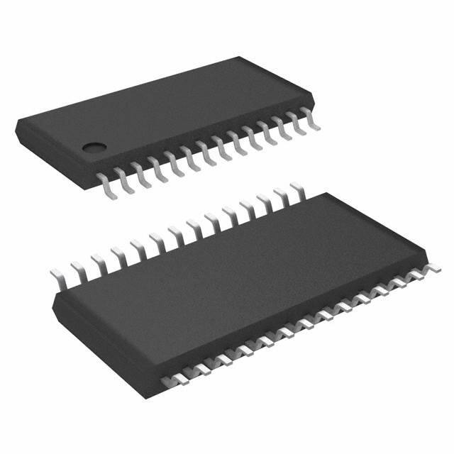
IDTCSPT855
2.5V PLL CLOCK DRIVER
COMMERCIAL AND INDUSTRIAL TEMPERATURE RANGES
2.5V PHASE LOCKED LOOP
CLOCK DRIVER
IDTCSPT855
FEATURES:
DESCRIPTION:
• PLL clock driver for DDR (Double Data Rate) synchronous
DRAM applications
• Spread spectrum clock compatible
• Operating frequency: 60MHz to 220MHz
• Low jitter (cycle-to-cycle): ±50ps
• Distributes one differential clock input to four differential clock
outputs
• Enters low power mode and 3-state outputs when input CLK
signal is less than 20MHz or PWRDWN is low
• Operates from a 2.5V supply
μA quiescent current
• Consumes 20MHz input signal, this detection circuit reactivates the PLL and
enables the outputs.
When AVDD is tied to GND, the PLL is turned off and bypassed for test
purposes. The CSPT855 is also able to track spread spectrum clocking for
reduced EMI.
Since the CSPT855 is based on PLL circuitry, it requires a stabilization time
to achieve phase-lock of the PLL. This stabilization time is required following
power up.
APPLICATIONS:
• For all DDR1 speeds: PC1600 (DDR200), PC2100 (DDR266),
PC2700 (DDR333), PC3200 (DDR400)
FUNCTIONAL BLOCK DIAGRAM
3
Y0
2
PWRDWN
AVDD
12
24
9
POWERDOWN
AND TEST
LOGIC
13
17
Y0
Y1
Y1
Y2
16
Y2
26
Y3
27
CLK
CLK
19
6
7
20
PLL
FBIN
23
FBIN
22
The IDT logo is a registered trademark of Integrated Device Technology, Inc.
COMMERCIAL AND INDUSTRIAL TEMPERATURE RANGES
Y3
FBOUT
FBOUT
NOVEMBER 2008
1
c
2008
Integrated Device Technology, Inc.
DSC-6203/12
�IDTCSPT855
2.5V PLL CLOCK DRIVER
COMMERCIAL AND INDUSTRIAL TEMPERATURE RANGES
PIN CONFIGURATION
ABSOLUTE MAXIMUM RATINGS(1)
GND
1
28
GND
Y0
2
27
Y3
Y0
3
26
Y3
VDDQ
4
25
VDDQ
GND
5
24
PWRDWN
CLK
6
23
FBIN
CLK
7
22
FBIN
VDDQ
8
21
VDDQ
AVDD
9
20
FBOUT
AGND
10
19
FBOUT
VDDQ
11
18
VDDQ
Y1
12
17
Y2
Y1
13
16
Y2
GND
14
15
GND
Symbol
Rating
VDDQ, AVDD
Supply Voltage Range
–0.5 to +3.6
V
VI(2)
VO(2)
Input Voltage Range
Output Voltage Range
–0.5 to VDDQ + 0.5
–0.5 to VDDQ + 0.5
V
V
IIK (VI < 0 or
VI < VDDQ)
Input Clamp Current
±50
mA
IOK (VO < 0 or
VO > VDDQ)
Output Clamp Current
±50
mA
Continuous Output Current
IO
(VO = 0 to VDDQ)
±50
mA
VDDQ or GND
θJA(3)
Continuous Current
Package Thermal Impedance
±100
105.8
mA
°C/W
TSTG
Storage Temperature Range
– 65 to +150
°C
PIN DESCRIPTION
Pin Number
AGND
10
AV DD
9
CLK, CLK
6, 7
I/O
Description
Ground for analog supply
Analog supply
I
Differential clock input
FBIN, FBIN
22, 23
I
Feedback differential clock input
FBOUT, FBOUT
19, 20
O
Feedback differential clock output
GND
1, 5, 14, 15, 28
Ground
PWRDWN
24
VDDQ
4, 8, 11, 18, 21, 25
Y[0:3]
3, 12, 17, 26
O
Buffered output copies of input clock, CLK
Y[0:3]
2, 13, 16, 27
O
Buffered output copies of input clock, CLK
I
Unit
NOTES:
1. Stresses greater than those listed under ABSOLUTE MAXIMUM RATINGS may cause
permanent damage to the device. This is a stress rating only and functional operation
of the device at these or any other conditions above those indicated in the operational
sections of this specification is not implied. Exposure to absolute maximum rating
conditions for extended periods may affect reliability.
2. The input and output negative-voltage ratings may be exceeded if the input and output
clamp-current ratings are observed. This value is limited to 3.6V maximum.
3. The package thermal impedance is calculated in accordance with JESD 51.
TSSOP
TOP VIEW
Pin Name
Max
Control input to turn device in the power-down mode
I/O supply
2
�IDTCSPT855
2.5V PLL CLOCK DRIVER
COMMERCIAL AND INDUSTRIAL TEMPERATURE RANGES
FUNCTION TABLE(1)
INPUTS
AVDD
PWRDWN
GND
GND
X
X
OUTPUTS
CLK
CLK
Y
Y
FBOUT
FBOUT
PLL
H
L
H
H
H
L
L
H
H
L
H
Bypassed/OFF
L
H
L
Bypassed/OFF
L
L
L
H
H
L
Z
Z
Z
Z
OFF
Z
Z
Z
Z
OFF
2.5V (nom)
H
L
H
L
H
L
H
ON
2.5V (nom)
H
2.5V (nom)
X
H
L
H
L
H
L
ON
很抱歉,暂时无法提供与“CSPT855PGGI8”相匹配的价格&库存,您可以联系我们找货
免费人工找货