DATASHEET
ICS477-05
QUAD PLL WITH VCXO FOR HDTV
Description
Features
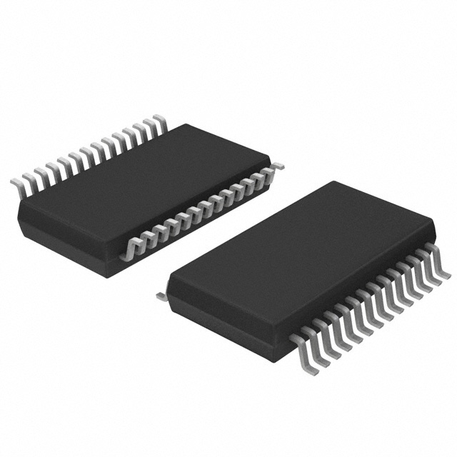
• Packaged in 28-pin SSOP (QSOP)
• Available in Pb-free packaging
• Replaces a VCXO plus multiple crystals and
The ICS477-05 generates five high-quality,
high-frequency clock outputs including two reference
outputs from a low frequency pullable crystal. It is
designed to replace crystals and crystal oscillators in
most electronic systems.
oscillators
• On-chip patented VCXO pull range 200 ppm
(minimum)
Using Phase-Locked-Loop (PLL) techniques, the
device runs from a fundamental mode, pullable crystal.
It can replace multiple crystals and oscillators, saving
board space and cost.
•
•
•
•
•
•
Duty cycle of 45/55
Operating voltage of 3.3V
Advanced, low power, CMOS process
Input crystal frequency of 27 MHz
Five output clocks
Industrial temperature range available
Block Diagram
VDD
6
VIN
54.054M
27 MHz
Pullable
Crystal
X1
X2
PLLA
Voltage
Controlled
Crystal
Oscillator
Divide
Logic
and
Output
Enable
Control
PLLB
PLLC
74.175M
54M
External capacitors
may be required
PLLD
2
27M
10
PDTS
IDT™ / ICS™ QUAD PLL WITH VCXO FOR HDTV
1
GND
ICS477-05
REV H 062404
�ICS477-05
QUAD PLL WITH VCXO FOR HDTV
VCXO AND SYNTHESIZER
Pin Assignment
X1
1
28
X2
GND
GND
V IN
VDD
VDD
2
3
4
5
6
27
26
25
24
23
VDD
PDTS
GND
VDD
VDD
GND
7
22
VDD
GND
8
21
GND
GND
GND
9
10
20
19
GND
GND
5 4 .0 5 4 M
NC
11
18
54M
12
17
NC
NC
7 4 .1 7 5 M
13
14
16
15
27M
27M
2 8 p in (1 5 0 m il) S S O P
Pin Descriptions
Pin
Number
Pin
Name
Pin Type
Pin Description
1
XI
Input
Crystal connection. Connect to a 27 MHz fundamental mode pullable crystal.
2
GND
Power
Connect to ground.
3
GND
Power
Connect to ground.
4
VIN
Input
VCXO Voltage input. Zero to 3.3 V analog control voltage for VCXO.
5, 6, 22, 23,
24, 27
VDD
Power
Connect to +3.3 V.
7, 8, 9, 10, 19,
20, 21
GND
Power
Connect to ground.
11
54.054M
Output
54.054 MHz clock output. Weak internal pull-down when tri-state.
12, 13, 17
NC
-
14
74.175M
Output
74.175 MHz clock output. Weak internal pull-down when tri-state.
15, 16
27M
Output
27 MHz reference clock output. Weak internal pull-down when tri-state.
18
54M
Output
54 MHz clock output. Weak internal pull-down when tri-state.
25
GND
Power
Connect to ground.
26
PDTS
Input
Powers down entire chip. Tri-states CLK outputs when low. Internal pull-up.
28
X2
Input
Crystal connection. Connect to a 27 MHz fundamental mode pullable crystal.
IDT™ / ICS™ QUAD PLL WITH VCXO FOR HDTV
No connect. Do not connect anything to these pins.
2
ICS477-05
REV H 062404
�ICS477-05
QUAD PLL WITH VCXO FOR HDTV
VCXO AND SYNTHESIZER
External Components
Crystal Tuning Load Capacitors
The crystal traces should include pads for small fixed
capacitors, one between X1 and ground, and another
between X2 and ground. Stuffing of these capacitors on
the PCB is optional. The need for these capacitors is
determined at system prototype evaluation, and is
influenced by the particular crystal used (manufacture
and frequency) and by PCB layout. The typical required
capacitor value is 1 to 4 pF.
The ICS477-05 requires a minimum number of external
components for proper operation.
Decoupling Capacitors
Decoupling capacitors of 0.01µF must be connected
between VDD and GND, as close to these pins as
possible. For optimum device performance, the
decoupling capacitors should be mounted on the
component side of the PCB. Avoid the use of vias in the
decoupling circuit.
To determine the need for and value of the crystal
adjustment capacitors, you will need a PC board of your
final layout, a frequency counter capable of about 1 ppm
resolution and accuracy, two power supplies, and some
samples of the crystals which you plan to use in
production, along with measured initial accuracy for
each crystal at the specified crystal load capacitance,
CL.
Series Termination Resistor
When the PCB trace between the clock outputs and the
loads are over 1 inch, series termination should be
used. To series terminate a 50Ω trace (a commonly
used trace impedance) place a 33Ω resistor in series
with the clock line, as close to the clock output pin as
possible. The nominal impedance of the clock output is
20Ω.
To determine the value of the crystal capacitors:
1. Connect VDD of the ICS477-05 to 3.3 V. Connect pin
4 of the ICS477-05 to the second power supply. Adjust
the voltage on pin 3 to 0V. Measure and record the
frequency of the 27 MHz output.
Quartz Crystal
The ICS477-05 VCXO function consists of the external
crystal and the integrated VCXO oscillator circuit. To
assure the best system performance (frequency pull
range) and reliability, a crystal device with the
recommended parameters (shown below) must be
used, and the layout guidelines discussed in the
following section must be followed.
2. Adjust the voltage on pin 4 to 3.3 V. Measure and
record the frequency of the same output.
To calculate the centering error:
The frequency of oscillation of a quartz crystal is
determined by its “cut” and by the load capacitors
connected to it. The ICS477-05 incorporates on-chip
variable load capacitors that “pull” (change) the
frequency of the crystal. The crystal specified for use
with the ICS477-05 is designed to have zero frequency
error when the total of on-chip + stray capacitance is 14
pF.
6 ( f 3.0V – f t arg et ) + ( f 0V – f t arg et )
Error = 10 x ------------------------------------------------------------------------------ – error xtal
f t arg et
Where:
ftarget = nominal crystal frequency
The external crystal must be connected as close to the
chip as possible and should be on the same side of the
PCB as the ICS477-05. There should be no via’s
between the crystal pins and the X1 and X2 device pins.
There should be no signal traces underneath or close to
the crystal.
errorxtal =actual initial accuracy (in ppm) of the crystal
being measured
If the centering error is less than ±25 ppm, no
adjustment is needed. If the centering error is more than
25 ppm negative, the PC board has excessive stray
capacitance and a new PCB layout should be
See application note MAN05 for complete crystal
specifications.
IDT™ / ICS™ QUAD PLL WITH VCXO FOR HDTV
3
ICS477-05
REV H 062404
�ICS477-05
QUAD PLL WITH VCXO FOR HDTV
VCXO AND SYNTHESIZER
2 x (centering error)/(trim sensitivity)
considered to reduce stray capacitance. (Alternately,
the crystal may be re-specified to a higher load
capacitance. Contact ICS for details.) If the centering
error is more than 25 ppm positive, add identical fixed
centering capacitors from each crystal pin to ground.
The value for each of these caps (in pF) is given by:
Trim sensitivity is a parameter which can be supplied by
your crystal vendor. If you do not know the value,
assume it is 30 ppm/pF. After any changes, repeat the
measurement to verify that the remaining error is
acceptably low (typically less than ±25 ppm).
External Capacitor =
PCB Layout Recommendations
spaces, instead they should be separated and away
from other traces.
For optimum device performance and lowest output
phase noise, the following guidelines should be
observed.
3) To minimize EMI, the 33Ω series termination resistor
(if needed) should be placed close to the clock output.
1) The 0.01µF decoupling capacitors should be
mounted on the component side of the board as close
to the VDD pins as possible. No vias should be used
between the decoupling capacitors and VDD pins. The
PCB trace to VDD pin should be kept as short as
possible, as should the PCB trace to the ground via.
4) An optimum layout is one with all components on the
same side of the board, minimizing vias through other
signal layers. Other signal traces should be routed away
from the ICS477-05. This includes signal traces just
underneath the device, or on layers adjacent to the
ground plane layer used by the device.
2) The external crystal should be mounted just next to
the device with short traces. The X1 and X2 traces
should not be routed next to each other with minimum
Absolute Maximum Ratings
Stresses above the ratings listed below can cause permanent damage to the ICS477-05. These ratings,
which are standard values for ICS commercially rated parts, are stress ratings only. Functional operation of
the device at these or any other conditions above those indicated in the operational sections of the
specifications is not implied. Exposure to absolute maximum rating conditions for extended periods can
affect product reliability. Electrical parameters are guaranteed only over the recommended operating
temperature range.
Item
Rating
Supply Voltage, VDD
7V
All Inputs and Outputs
-0.5 V to VDD+0.5 V
Ambient Operating Temperature (commercial)
0 to +70° C
Ambient Operating Temperature (industrial)
-40 to +85° C
Storage Temperature
-65 to +150° C
Junction Temperature
125° C
Soldering Temperature
260° C
IDT™ / ICS™ QUAD PLL WITH VCXO FOR HDTV
4
ICS477-05
REV H 062404
�ICS477-05
QUAD PLL WITH VCXO FOR HDTV
VCXO AND SYNTHESIZER
Recommended Operation Conditions
Parameter
Min.
Ambient Operating Temperature
Typ.
Max.
Units
+85
°C
+3.45
V
-40
Power Supply Voltage (measured in respect to GND)
+3.15
+3.3
DC Electrical Characteristics
Unless stated otherwise, VDD = 3.3 V ±5%, Ambient Temperature -40 to +85° C
Parameter
Symbol
Conditions
Min.
Typ.
Max.
Units
3.15
3.3
3.45
V
Operating Voltage
VDD
Supply Current
IDD
No load
48
mA
IDDPD
No load
0.5
mA
Power Down Current
Input High Voltage
VIH
PDTS pin
Input Low Voltage
VIL
PDTS pin
Output High Voltage
VOH
IOH = -4 mA
VDD-0.4
V
Output High Voltage
VOH
IOH = -12 mA
2.4
V
Output Low Voltage
VOL
IOL = 12 mA
Short Circuit Current
IOS
CLK output
Input Capacitance, inputs
2
V
0.8
0.4
V
V
±80
mA
CIN
5
pF
Nominal Output Impedance
ZOUT
20
Ω
Internal Pull-up Resistor
RPUP
PDTS pin
360
kΩ
Internal Pull-down Resistor
RPD
CLK outputs
510
kΩ
AC Electrical Characteristics
Unless stated otherwise, VDD = 3.3 V ±5%, Ambient Temperature -40 to +85° C
Parameter
Symbol
Conditions
Min.
Typ.
Max. Units
Input Frequency
fin
Crystal input, Note 2
27
Crystal Pullability
FP
0V< VIN < 3.3 V
VCXO Gain
K0
VIN = VDD/2 + 1 V
150
ppm/V
Output Rise Time
tOR
20% to 80%, Note 1
1.2
ns
Output Fall Time
tOF
80% to 20%, Note 1
1.0
ns
±100
ppm
Clock Stabilization Time after
Power-up
Cycle Jitter (short term jitter)
IDT™ / ICS™ QUAD PLL WITH VCXO FOR HDTV
MHz
10
±200
tja
5
ICS477-05
ms
ps
REV H 062404
�ICS477-05
QUAD PLL WITH VCXO FOR HDTV
Parameter
VCXO AND SYNTHESIZER
Symbol
Long Term Jitter
Conditions
Min.
Typ.
Max. Units
54.054M, 54M clocks
1.0
ns
74.175M clock
1.3
ns
27M reference clock
300
ps
Output Enable Time
PDTS high to output
locked to ±1%
250
µs
Output Disable Time
PDTS low to tri-state
20
ns
Note 1: Measured with a 15 pF load.
Note 2:With an ICS approved crystal.
Marking Diagram
Marking Diagram (Pb free)
28
28
15
ICS477R-05
######
YYWW
ICS477R-05LF
######
YYWW
14
1
Marking Diagram (Pb free, industrial)
15
28
ICS477R-05I
######
YYWW
15
ICS477R-05ILF
######
YYWW
14
1
14
1
Marking Diagram (industrial)
28
15
14
1
Notes:
1. ###### is the lot code.
2. YYWW is the last two digits of the year, and the week.
3. “LF” designates Pb (lead) free.
4. “I” designates industrial temperature grade.
IDT™ / ICS™ QUAD PLL WITH VCXO FOR HDTV
6
ICS477-05
REV H 062404
�ICS477-05
QUAD PLL WITH VCXO FOR HDTV
VCXO AND SYNTHESIZER
Package Outline and Package Dimensions (28-pin SSOP, 150 Mil. Body)
Package dimensions are kept current with JEDEC Publication No. 95
28
Millimeters
Symbol
E1
A
A1
A2
b
C
D
E
E1
e
L
α
E
INDEX
AREA
1 2
D
Min
Inches
Max
Min
1.35
1.75
0.10
0.25
-1.50
0.20
0.30
0.18
0.25
9.80
10.00
5.80
6.20
3.80
4.00
0.635 Basic
0.40
1.27
0°
8°
Max
.053
.069
.0040
.010
-.059
0.008
0.012
.007
.010
.386
.394
.228
.244
.150
.157
0.025 Basic
.016
.050
0°
8°
A
A2
A1
c
-Ce
SEATING
PLANE
b
L
.10 (.004)
C
Ordering Information
Part / Order Number
Marking
Shipping Packaging
Package
Temperature
477R-05
477R-05T
477R-05I
477R-05IT
477R-05LF
477R-05LFT
477R-05ILF
477R-05ILFT
ICS477R-05 (top line)
YYWW (3rd line)
ICS477R-05I (top line)
YYWW (3rd line)
ICS477R-05LF (top line)
YYWW (3rd line)
ICS477R-05ILF (top line)
YYWW (3rd line)
Tubes
Tape and Reel
Tubes
Tape and Reel
Tubes
Tape and Reel
Tubes
Tape and Reel
28-pin SSOP
28-pin SSOP
28-pin SSOP
28-pin SSOP
28-pin SSOP
28-pin SSOP
28-pin SSOP
28-pin SSOP
0 to +70° C
0 to +70° C
-40 to +85° C
-40 to +85° C
0 to +70° C
0 to +70° C
-40 to +85° C
-40 to +85° C
“LF” denotes Pb (lead) free package.
While the information presented herein has been checked for both accuracy and reliability, Integrated Circuit Systems (ICS)
assumes no responsibility for either its use or for the infringement of any patents or other rights of third parties, which would result
from its use. No other circuits, patents, or licenses are implied. This product is intended for use in normal commercial
applications. Any other applications such as those requiring extended temperature range, high reliability, or other extraordinary
environmental requirements are not recommended without additional processing by ICS. ICS reserves the right to change any
circuitry or specifications without notice. ICS does not authorize or warrant any ICS product for use in life support devices or
critical medical instruments.
IDT™ / ICS™ QUAD PLL WITH VCXO FOR HDTV
7
ICS477-05
REV H 062404
�ICS477-05
QUAD PLL WITH VCXO FOR HDTV
VCXO AND SYNTHESIZER
Innovate with IDT and accelerate your future networks. Contact:
www.IDT.com
For Sales
For Tech Support
800-345-7015
408-284-8200
Fax: 408-284-2775
Corporate Headquarters
Asia Pacific and Japan
Europe
Integrated Device Technology, Inc.
6024 Silver Creek Valley Road
San Jose, CA 95138
United States
800 345 7015
+408 284 8200 (outside U.S.)
Integrated Device Technology
Singapore (1997) Pte. Ltd.
Reg. No. 199707558G
435 Orchard Road
#20-03 Wisma Atria
Singapore 238877
+65 6 887 5505
IDT Europe, Limited
Prime House
Barnett Wood Lane
Leatherhead, Surrey
United Kingdom KT22 7DE
+44 1372 363 339
© 2006 Integrated Device Technology, Inc. All rights reserved. Product specifications subject to change without notice. IDT and the IDT logo are trademarks of Integrated Device
Technology, Inc. Accelerated Thinking is a service mark of Integrated Device Technology, Inc. All other brands, product names and marks are or may be trademarks or registered
trademarks used to identify products or services of their respective owners.
Printed in USA
�IMPORTANT NOTICE AND DISCLAIMER
RENESAS ELECTRONICS CORPORATION AND ITS SUBSIDIARIES (“RENESAS”) PROVIDES TECHNICAL
SPECIFICATIONS AND RELIABILITY DATA (INCLUDING DATASHEETS), DESIGN RESOURCES (INCLUDING
REFERENCE DESIGNS), APPLICATION OR OTHER DESIGN ADVICE, WEB TOOLS, SAFETY INFORMATION, AND
OTHER RESOURCES “AS IS” AND WITH ALL FAULTS, AND DISCLAIMS ALL WARRANTIES, EXPRESS OR IMPLIED,
INCLUDING, WITHOUT LIMITATION, ANY IMPLIED WARRANTIES OF MERCHANTABILITY, FITNESS FOR A
PARTICULAR PURPOSE, OR NON-INFRINGEMENT OF THIRD PARTY INTELLECTUAL PROPERTY RIGHTS.
These resources are intended for developers skilled in the art designing with Renesas products. You are solely responsible
for (1) selecting the appropriate products for your application, (2) designing, validating, and testing your application, and (3)
ensuring your application meets applicable standards, and any other safety, security, or other requirements. These
resources are subject to change without notice. Renesas grants you permission to use these resources only for
development of an application that uses Renesas products. Other reproduction or use of these resources is strictly
prohibited. No license is granted to any other Renesas intellectual property or to any third party intellectual property.
Renesas disclaims responsibility for, and you will fully indemnify Renesas and its representatives against, any claims,
damages, costs, losses, or liabilities arising out of your use of these resources. Renesas' products are provided only subject
to Renesas' Terms and Conditions of Sale or other applicable terms agreed to in writing. No use of any Renesas resources
expands or otherwise alters any applicable warranties or warranty disclaimers for these products.
(Rev.1.0 Mar 2020)
Corporate Headquarters
Contact Information
TOYOSU FORESIA, 3-2-24 Toyosu,
Koto-ku, Tokyo 135-0061, Japan
www.renesas.com
For further information on a product, technology, the most
up-to-date version of a document, or your nearest sales
office, please visit:
www.renesas.com/contact/
Trademarks
Renesas and the Renesas logo are trademarks of Renesas
Electronics Corporation. All trademarks and registered
trademarks are the property of their respective owners.
© 2020 Renesas Electronics Corporation. All rights reserved.
�


 工商网监
湘ICP备2023018690号
工商网监
湘ICP备2023018690号
