PRELIMINARY
ICS8733-01
Integrated
Circuit
Systems, Inc.
700MHZ FORWARD ERROR CORRECTION
DIFFERENTIAL-TO-3.3V LVPECL CLOCK GENERATOR
GENERAL DESCRIPTION
FEATURES
The ICS8733-01 is a dual output, Differentialto-3.3V LVPECL Clock Generator and a
HiPerClockS™
member of the HiPerClockS™ family of High
Performance Clock Solutions from ICS. The
ICS8733-01 is designed to be used for applications utilizing Forward Error Correction (FEC) designs. The
ICS8733-01 generates a 14/15 or a 15/14 output clock based
upon the input reference clock in order to incorporate the
FEC capability required by the application.
• Clock synthesis of 14/15 or 15/14 of the input reference
clock to be utilized in Forward Error Correction (FEC)
applications
Clock generation is performed by a fully integrated and
low-jitter phase-locked loop. The ICS8733-01 accepts any
differential signal as its input with an input reference frequency range of 36.27MHz to 750MHz. There are two
LVPECL outputs which can generate output frequencies of
38.88MHz to 700MHz.
• Output frequency range: 38.88MHz - 700MHz
,&6
• Fully integrated PLL
• 2 differential 3.3V LVPECL outputs
• 1 differential clock input pair
• CLK, nCLK pair can accept the following differential input
levels: LVPECL, LVHSTL, LVDS, SSTL, HCSL
• Input frequency range: 36.27MHz - 750MHz
• VCO range: 200MHz to 700MHz
• PLL bypass and test modes that support in-circuit testing
and on-chip functional block characterization
• Cycle-to-cycle jitter: 20ps (typical)
• Period jitter: TBD
• Output skew: 10ps (maximum)
• 3.3V supply voltage
• 0°C to 70°C ambient operating temperature
BLOCK DIAGRAM
PIN ASSIGNMENT
nc
nc
VCC
VCC
32 31 30 29 28 27 26 25
PLL_SEL
“N”
CLK
nCLK
nc
MR
nc
nc
DIV_SEL1
PLL_SEL
DIV_SEL0
÷14
÷15
0
nc
1
24
CLK
FEC_NSEL
2
23
n_CLK
FEC_MSEL
3
22
VCCA
VEE
4
21
VCCA
VEE
5
20
DIV_SEL0
TEST_SEL
6
19
DIV_SEL1
TEST_EN
7
18
nc
VEE
8
17
MR
1
FEC_NSEL
0
VEE
“M”
TEST
1
nFOUT0
0
FOUT0
÷14
VCCO
1
FOUT0
nFOUT0
nFOUT1
÷15
FOUT1
nFOUT1
FOUT1
0
00
01
10
11
VCC
1
9 10 11 12 13 14 15 16
÷¼
÷1
÷2
÷4
TEST
PLL
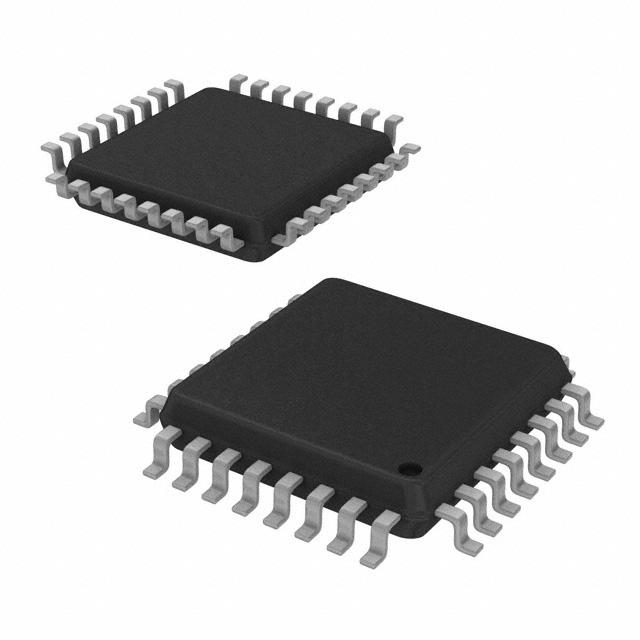
ICS8733-01
32-Lead LQFP
7mm x 7mm x 1.4mm package body
Y Package
Top View
FEC_MSEL
TEST_SEL
TEST_EN
The Preliminary Information presented herein represents a product in prototyping or pre-production. The noted characteristics are based on initial
product characterization. Integrated Circuit Systems, Incorporated (ICS) reserves the right to change any circuitry or specifications without notice.
8733BY-01
www.icst.com/products/hipercocks.html
1
REV. A JANUARY 17, 2002
�PRELIMINARY
Integrated
Circuit
Systems, Inc.
ICS8733-01
700MHZ FORWARD ERROR CORRECTION
DIFFERENTIAL-TO-3.3V LVPECL CLOCK GENERATOR
FUNCTIONAL DESCRIPTION
The ICS8733-01 features a fully integrated PLL and therefore requires no external component for setting the loop bandwidth.
The ICS8733-01 will generate an output having a frequency as follows:
fREF_CLK x M
N
The M and N bits are controlled by the FEC_NSEL and FEC_MSEL control pins as shown in Table 3A and Table 3B.
As a result, FOUT0 can be configured to have an output frequency equal to 14/15, 15/14, 14/14, or 15/15 of the reference
input frequency.
The second output clock (FOUT1) is configured to produce a frequency equal to FOUT0, FOUT/2, FOUT0/4, or FOUT0x4,
dependent upon the DIV_SEL0 and DIV_SEL1 bits as shown in Table 3C and 3D.
The reference input frequency range is dependent upon not only the M and N bits, but also upon the FOUT1 output
configuration which is determined by the DIV_SEL0 and DIV_SEL1 bits. Table 3C shows the possible FOUT0 and
FOUT1 output configurations as well as the reference input frequency range for each of these configurations.
The ICS8733-01 also supports in-circuit testing and on-chip functional block characterization via two test inputs and
one test output. With the ICS8733-01 in PLL bypass mode (PLL_SEL = 0), the reference input bypasses the PLL and
in-circuit testing of the N, M, and output dividers can take place. Table 3D shows the output configurations for the
different combinations of the DIV_SEL1 and DIV_SEL0 pins.
8733BY-01
www.icst.com/products/hipercocks.html
2
REV. A JANUARY 17, 2002
�PRELIMINARY
ICS8733-01
Integrated
Circuit
Systems, Inc.
700MHZ FORWARD ERROR CORRECTION
DIFFERENTIAL-TO-3.3V LVPECL CLOCK GENERATOR
TABLE 1. PIN DESCRIPTIONS
Number
Name
Type
Description
1, 18,
25, 26,
30, 31, 32
2
nc
Unused
FEC_NSEL
Input
Pulldown Selects the N divide value. LVCMOS / LVTTL interface levels.
3
FEC_MSEL
Input
Pulldown Selects the M divide value. LVCMOS / LVTTL interface levels.
4, 5, 8, 16
VEE
Power
6
TEST_SEL
Input
7
TEST_EN
Input
Negative supply pins. Connect to ground.
Configures the TEST output pin to one of two different test modes.
Pulldown
LVCMOS / LVTTL interface levels.
Pulldown Enables the TEST output pin. LVCMOS / LVTTL interface levels.
9
TEST
Output
Output test pin. Programmed using TEST_SEL pin as shown in Table 3D.
10, 28, 29
VCC
FOUT1,
nFOUT1
VCCO
FOUT0,
nFOUT0
Power
Positive supply pins. Connect to 3.3V.
Output
Differential output for the generator. 3.3V LVPECL interface levels.
Power
Output supply pin. Connect to 3.3V.
Output
Differential ouput for the generator. 3.3V LVPECL interface levels.
11, 12
13
14, 15
17
MR
Input
19, 20
DIV_SEL1,
DIV_SEL0
Input
21, 22
VCCA
Power
23
nCLK
Input
24
CLK
Input
No connect.
Resets the M, N, and output divider. Forces FOUT0 and FOUT1 low.
LVCMOS / LVTTL interface levels.
Determines the output divide value for FOUT1.
Pulldown
LVCMOS / LVTTL interface levels.
Pulldown
Analog supply pins. Connect to 3.3V.
Pullup
Inver ting differential clock input.
Pulldown Non-inver ting differential clock input.
Determines whether generator is in PLL or bypass mode.
LVCMOS / LVTTL interface levels.
NOTE: Pullup and Pulldown refer to internal input resistors. See Table 2, Pin Characteristics, for typical values.
27
PLL_SEL
Input
Pullup
TABLE 2. PIN CHARACTERISTICS
Symbol
Parameter
Test Conditions
Minimum
Typical
Maximum
Units
CIN
Input Capacitance
RPULLUP
Input Pullup Resistor
51
KΩ
RPULLDOWN
Input Pulldown Resistor
51
KΩ
8733BY-01
4
www.icst.com/products/hipercocks.html
3
pF
REV. A JANUARY 17, 2002
�PRELIMINARY
ICS8733-01
Integrated
Circuit
Systems, Inc.
700MHZ FORWARD ERROR CORRECTION
DIFFERENTIAL-TO-3.3V LVPECL CLOCK GENERATOR
TABLE 3A. FEC_NSEL TRUTH TABLE
TABLE 3B. FEC-MSEL TRUTH TABLE
FEC_NSEL
N
FEC_MSEL
M
0
14
0
15
1
15
1
14
TABLE 3C. OUTPUT CONFIGURATION
AND INPUT
FREQUENCY RANGE TABLE
Reference Input Frequency Range (MHz)
Minimum
Input
DIV_SEL1 DIV_SEL0 FEC_NSEL FEC_MSEL
Frequency
(MHz)
0
0
0
0
36.27
Maximum
Minimum Maximum Minimum Maximum
Input
FOUT0
FOUT0
FOUT1
FOUT1
Frequency
(MHz)
(MHz)
(MHz)
(MHz)
(MHz)
81.67
38.86
87.50
155.44
350
0
0
0
1
36.27
87.5
36.27
87.50
145.08
350
0
0
1
0
38.88
87.5
38.88
87.50
155.52
350
0
0
1
1
38.88
93.75
36.29
87.50
145.15
350
0
1
0
0
93.3
326.67
100
350
100
350
0
1
0
1
100
350
100
350
100
350
0
1
1
0
100
350
100
350
100
350
0
1
1
1
107
375
100
350
100
350
1
0
0
0
186.7
653.33
200
700
100
350
1
0
0
1
200
700
200
700
100
350
1
0
1
0
200
700
200
700
100
350
1
0
1
1
214.3
750
200
700
100
350
1
1
0
0
186.7
653.33
200
700
50
175
1
1
0
1
200
700
200
700
50
175
1
1
1
0
200
700
200
700
50
175
1
1
1
1
214.3
750
200
700
50
175
TABLE 3D. OUTPUT CONFIGURATION TABLE
AND
TEST MODE OPERATION
PLL_SEL = 1
DIV_SEL1
DIV_SEL0
0
PLL_SEL = 0 and TEST_EN = 1
FOUT0
FOUT1
FOUT0
FOUT1
TEST
TEST_SEL = 0
TEST
TEST_SEL = 1
0
fREFxM/N
fREFx4M/N
fREF/4N
fREF/N
2fREF/N
fREF/2MN
0
1
fREFxM/N
fREFxM/N
fREF/N
fREF/N
2fREF/N
2fREF/MN
1
0
fREFxM/N
fREFx2M/N
fREF/N
fREF/2N
fREF/N
fREF/MN
1
1
fREFxM/N
fREFx4M/N
fREF/N
fREF/4N
fREF/N
fREF/MN
NOTE: In bypass mode, FOUT0 and FOUT1 will not always result in a 50% duty cycle.
Test output will never be 50% duty cycle.
8733BY-01
www.icst.com/products/hipercocks.html
4
REV. A JANUARY 17, 2002
�PRELIMINARY
ICS8733-01
Integrated
Circuit
Systems, Inc.
700MHZ FORWARD ERROR CORRECTION
DIFFERENTIAL-TO-3.3V LVPECL CLOCK GENERATOR
ABSOLUTE MAXIMUM RATINGS
Supply Voltage, VCC
Inputs, VCC
Outputs, VCCO
Package Thermal Impedance, θJA
Storage Temperature, TSTG
X
4.6V
-0.5V to VCC + 0.5 V
-0.5V to VCCO + 0.5V
47.9°C/W (0 lfpm)
-65°C to 150°C
Stresses beyond those listed under Absolute Maximum Ratings may cause permanent damage to the device. These ratings are
stress specifications only. Functional operation of product at these conditions or any conditions beyond those listed in the DC
Characteristics or AC Characteristics is not implied. Exposure to absolute maximum rating conditions for extended periods may
affect product reliability.
TABLE 4A. POWER SUPPLY DC CHARACTERISTICS, VCC = VCCA = VCCO = 3.3V±5%, TA = 0°C TO 70°C
Symbol
Parameter
Test Conditions
Minimum
Typical
Maximum
Units
VCC
Positive Supply Voltage
3.135
3.3
3.465
V
VCCA
Analog Supply Voltage
3.135
3.3
3.465
V
VCCO
Output Supply Voltage
3.135
3.3
3.465
V
IEE
Power Supply Current
TBD
mA
ICCA
Analog Supply Current
TBD
mA
TABLE 4B. LVCMOS/LVTTL DC CHARACTERISTICS, VCC = VCCA = VCCO = 3.3V±5%, TA = 0°C TO 70°C
Symbol
Parameter
VIH
Input
High Voltage
VIL
Input
Low Voltage
IIH
Input
High Current
IIL
Input
Low Current
Test Conditions
FEC_NSEL, FEC_MSEL,
TEST_SEL, TEST_EN,
DIV_SELx, PLL_SEL, MR
FEC_NSEL, FEC_MSEL,
TEST_SEL, TEST_EN,
DIV_SELx, PLL_SEL, MR
FEC_NSEL, FEC_MSEL,
TEST_SEL, TEST_EN,
DIV_SELx, MR
PLL_SEL
FEC_NSEL, FEC_MSEL,
TEST_SEL, TEST_EN,
DIV_SELx, MR
PLL_SEL
Minimum
Typical
Maximum
Units
2
VCC + 0.3
V
-0.3
0.8
V
VCC = VIN = 3.465V
150
µA
VCC = VIN = 3.465V
5
µA
VCC = 3.465V, VIN = 0V
-5
µA
VCC = 3.465V, VIN = 0V
-150
µA
Output
VOH
TEST; NOTE 1
2.6
High Voltage
Output
VOL
TEST; NOTE 1
Low Voltage
NOTE 1: Outputs terminated with 50Ω to VCCO/2. See page 7, Figure 1, 3.3V Output Load Test Circuit.
8733BY-01
www.icst.com/products/hipercocks.html
5
V
0.5
V
REV. A JANUARY 17, 2002
�PRELIMINARY
ICS8733-01
Integrated
Circuit
Systems, Inc.
700MHZ FORWARD ERROR CORRECTION
DIFFERENTIAL-TO-3.3V LVPECL CLOCK GENERATOR
TABLE 4C. DIFFERENTIAL DC CHARACTERISTICS, VCC = VCCA = VCCO = 3.3V±5%, TA = 0°C TO 70°C
Symbol Parameter
Test Conditions
Minimum
Typical
Maximum
Units
CLK
VCC = VIN = 3.465V
150
µA
nCLK
VCC = VIN = 3.465V
5
µA
CLK
VCC = 3.465V, VIN = 0V
-5
µA
nCLK
VCC = 3.465V, VIN = 0V
-150
µA
IIH
Input High Current
IIL
Input Low Current
VPP
Peak-to-Peak Input Voltage
0.15
VCMR
Common Mode Input Voltage; NOTE 1, 2
VEE + 0.5
NOTE 1: Common mode voltage is defined as VIH.
NOTE 2: For single ended applications, the maximum input voltage for CLK, nCLK is VCC + 0.3V.
1.3
V
VCC + 0.85
V
TABLE 4D. LVPECL DC CHARACTERISTICS, VCC = VCCA = VCCO = 3.3V±5%, TA = 0°C TO 70°C
Symbol
Parameter
Maximum
Units
VOH
Output High Voltage; NOTE 1
Test Conditions
Minimum
VCCO - 1.4
Typical
VCCO - 1.0
V
VOL
Output Low Voltage; NOTE 1
VCCO - 2.0
VCCO -1.7
V
VSWING
Peak-to-Peak Output Voltage Swing
0.6
0.85
V
Maximum
Units
750
MHz
NOTE 1: Outputs terminated with 50 Ω to VCCO - 2V.
TABLE 5. INPUT FREQUENCY CHARACTERISTICS, VCC = VCCA = VCCO = 3.3V±5%, TA = 0°C TO 70°C
Symbol Parameter
fIN
Test Conditions
Input Frequency
Minimum
Typical
36.27
TABLE 6. AC CHARACTERISTICS, VCC = VCCA = VCCO = 3.3V±5%, TA = 0°C TO 70°C
Symbol
Parameter
Test Conditions
FOUT
Output Frequency
tjit(cc)
Cycle-to-Cycle Jitter, RMS; NOTE 1, 3
tjit(per)
Period Jitter, RMS; NOTE 1, 3
tsk(o)
Output Skew; NOTE 2, 3
tR
Output Rise Time
odc
Output Duty Cycle
Minimum
Typical
38.88
Maximum
Units
700
MHz
20
ps
TBD
ps
10
ps
700
ps
PLL Lock Time
10
tLOCK
All parameters measured at 500MHz unless noted otherwise.
NOTE 1: The cycle-to-cycle jitter on the input will equal the jitter on the output. The par t does not add jitter.
NOTE 2: Defined as skew between outputs at the same supply voltage and with equal load conditions.
Measured at the output differential cross points.
NOTE 3: This parameter is defined in accordance with JEDEC Standard 65.
ms
8733BY-01
20% to 80% @ 50MHz
300
50
www.icst.com/products/hipercocks.html
6
%
REV. A JANUARY 17, 2002
�PRELIMINARY
ICS8733-01
Integrated
Circuit
Systems, Inc.
700MHZ FORWARD ERROR CORRECTION
DIFFERENTIAL-TO-3.3V LVPECL CLOCK GENERATOR
PARAMETER MEASUREMENT INFORMATION
VCC, VCCA, VCCO
SCOPE
Qx
LVPECL
VCC, VCCA, VCCO = 2V
nQx
VEE = -1.3V ± 0.135V
FIGURE 1 - 3.3V OUTPUT LOAD TEST CIRCUIT
V CC
nCLK
V
PP
Cross Points
V
CMR
CLK
VEE
FIGURE 2 - DIFFERENTIAL INPUT LEVEL
8733BY-01
www.icst.com/products/hipercocks.html
7
REV. A JANUARY 17, 2002
�PRELIMINARY
ICS8733-01
Integrated
Circuit
Systems, Inc.
700MHZ FORWARD ERROR CORRECTION
DIFFERENTIAL-TO-3.3V LVPECL CLOCK GENERATOR
nFOUTx
FOUTx
nFOUTy
FOUTy
tsk(o)
FIGURE 3 - OUTPUT SKEW
nFOUT0, nFOUT1
FOUT0, FOUT1
➤
tcycle
➤
n
tcycle
n+1
➤
➤
t jit(cc) = tcycle n –tcycle n+1
1000 Cycles
FIGURE 4 - Cycle-to-Cycle Jitter
VOH
Vref
VOL
1σ contains 68.26% of all measurements
2σ contains 95.4% of all measurements
3σ contains 99.73% of all measurements
4σ contains 99.99366% of all measurements
6σ contains (100-1.973x10⁻⁷)% of all measurements
Histogram
Reference Point
Mean Period
(Trigger Edge)
(First edge after trigger)
FIGURE 5 - Period Jitter
8733BY-01
www.icst.com/products/hipercocks.html
8
REV. A JANUARY 17, 2002
�PRELIMINARY
ICS8733-01
Integrated
Circuit
Systems, Inc.
700MHZ FORWARD ERROR CORRECTION
DIFFERENTIAL-TO-3.3V LVPECL CLOCK GENERATOR
80%
80%
V
20%
Clock Inputs
and Outputs
SWING
20%
t
t
R
FIGURE 6 - INPUT
AND
OUTPUT RISE
AND
F
FALL TIME
nFOUT0, nFOUT1
TEST, FOUT0, FOUT1
Pulse Width
t
t
odc =
t
PERIOD
PW
PERIOD
FIGURE 7 - odc & tPERIOD
8733BY-01
www.icst.com/products/hipercocks.html
9
REV. A JANUARY 17, 2002
�PRELIMINARY
ICS8733-01
Integrated
Circuit
Systems, Inc.
700MHZ FORWARD ERROR CORRECTION
DIFFERENTIAL-TO-3.3V LVPECL CLOCK GENERATOR
APPLICATION INFORMATION
WIRING THE DIFFERENTIAL INPUT TO ACCEPT SINGLE ENDED LEVELS
Figure 8 shows how the differential input can be wired to accept single ended levels. The reference voltage V_REF = VCC/2 is
generated by the bias resistors R1, R2 and C1. This bias circuit should be located as close as possible to the input pin. The ratio of
R1 and R2 might need to be adjusted to position the V_REF in the center of the input voltage swing. For example, if the input clock
swing is only 2.5V and VCC = 3.3V, V_REF should be 1.25V and R2/R1 = 0.609.
VCC
R1
1K
CLK_IN
+
V_REF
-
C1
0.1uF
R2
1K
FIGURE 8 - SINGLE ENDED SIGNAL DRIVING DIFFERENTIAL INPUT
8733BY-01
www.icst.com/products/hipercocks.html
10
REV. A JANUARY 17, 2002
�PRELIMINARY
ICS8733-01
Integrated
Circuit
Systems, Inc.
700MHZ FORWARD ERROR CORRECTION
DIFFERENTIAL-TO-3.3V LVPECL CLOCK GENERATOR
POWER SUPPLY FILTERING TECHNIQUES
As in any high speed analog circuitry, the power supply pins
are vulnerable to random noise. The ICS8733-01 provides
separate power supplies to isolate any high switching
noise from the outputs to the internal PLL. VCC, VCCA, and VCCO
should be individually connected to the power supply
plane through vias, and bypass capacitors should be
used for each pin. To achieve optimum jitter performance,
power supply isolation is required. Figure 9 illustrates how
a 10Ω resistor along with a 10µF and a .01µF bypass
capacitor should be connected to each VCCA pin.
3.3V
VCC
.01µF
10 Ω
VCCA
.01µF
10 µF
FIGURE 9 - POWER SUPPLY FILTERING
TERMINATION FOR LVPECL OUTPUTS
50Ω transmission lines. Matched impedance techniques should
be used to maximize operating frequency and minimize signal
distortion. There are a few simple termination schemes. Figures
10A and 10B show two different layouts which are recommended
only as guidelines. Other suitable clock layouts may exist and it
would be recommended that the board designers simulate to guarantee compatibility across all printed circuit and clock component process variations.
The clock layout topology shown below is a typical termination for LVPECL outputs. The two different layouts mentioned
are recommended only as guidelines.
FOUT and nFOUT are low impedance follower outputs that generate ECL/LVPECL compatible outputs. Therefore, terminating
resistors (DC current path to ground) or current sources must
be used for functionality. These outputs are designed to drive
3.3V
Zo = 50Ω
5
2 Zo
FOUT
Zo = 50Ω
FOUT
50 Ω
(VOH + VOL / VCC –2) –2
VCC - 2V
RTT
3
2 Zo
Zo
FIGURE 10A - LVPECL OUTPUT TERMINATION
8733BY-01
FIN
50Ω
➤
1
RTT =
5
2 Zo
FIN
3
2 Zo
FIGURE 10B - LVPECL OUTPUT TERMINATION
www.icst.com/products/hipercocks.html
11
REV. A JANUARY 17, 2002
�PRELIMINARY
ICS8733-01
Integrated
Circuit
Systems, Inc.
700MHZ FORWARD ERROR CORRECTION
DIFFERENTIAL-TO-3.3V LVPECL CLOCK GENERATOR
LAYOUT GUIDELINE
The schematic of the ICS8733-01 layout example used in this layout guideline is shown in Figure 11A. The ICS8733-01 recommended PCB board layout for this example is shown in Figure 11B. This layout example is used as a general guideline. The layout in
the actual system will depend on the selected component types, the density of the components, the density of the traces, and the
stacking of the P.C. board.
VCC
SP = Space (i.e. not intstalled)
RU1
SP
RU2
SP
RU3
1K
RU4
SP
RU5
SP
RU6
1K
RU7
SP
3.3V
FEC_NSEL
FEC_MSEL
PLL_SEL
TEST_SEL
TEST_EN
DIV_SEL0
DIV_SEL1
Fin = 155.52 MHz
Zo = 50 Ohm
CLK
Zo = 50 Ohm
nCLK
3.3V LVPECL
RD2
1K
RD3
SP
RD4
1K
RD5
1K
RD6
SP
RD7
1K
PLL_SEL
RD1
1K
Fout = Fin x (15/14)
FEC_NSEL
FEC_MSEL
FEC_NSEL=0 (Divide by 14)
FEC_MSEL=0 (Divide by 15)
TEST_SEL
TEST_EN
REF_CLK
nREF_CLK
VCCA
VCCA
DIV_SEL0
DIV_SEL1
NC
MR
NC
FEC_NSEL
FEC_MSEL
VEE
VEE
TEST_SEL
TEST_EN
VEE
24
23
22
21
20
19
18
17
VCC
R7
VCCA
DIV_SEL0
DIV_SEL1
10
C12
0.01u
C11
0.01u
C16
10u
See Data Sheet for other
configurations
VCCO
8733-01
9
10
11
12
13
14
15
16
TEST
VCC
FOUT1
nFOUT1
VCCO
FOUT0
nFOUT0
VEE
DIV_SEL[1:0]=01
1
2
3
4
5
6
7
8
R1
50
R3
50
32
31
30
29
28
27
26
25
In this example:
NC
NC
NC
VCC
VCC
PLL_SEL
NC
NC
U2
Fin = 155.52 MHz
Fout = 166.63 MHz
R2
50
Fout = 166.63 MHz
Zo = 50 Ohm
VCC=3.3V
FOUT0
IN+
VCCO=3.3V
C15
0.1u
TL1
Zo = 50 Ohm
Bypass capacitor located near
the power pins
IN-
nFOUT0
TL2
(U1-10) VCC
C1
0.1uF
(U1-28)
R2
50
(U1-29)
C2
0.1uF
R1
50
C3
0.1uF
R3
50
FIGURE 11A - SCHEMATIC
8733BY-01
OF
RECOMMENDED LAYOUT
www.icst.com/products/hipercocks.html
12
REV. A JANUARY 17, 2002
�PRELIMINARY
ICS8733-01
Integrated
Circuit
Systems, Inc.
700MHZ FORWARD ERROR CORRECTION
DIFFERENTIAL-TO-3.3V LVPECL CLOCK GENERATOR
The following component footprints are used in this layout
example:
trace delay might be restricted by the available space on the board
and the component location. While routing the traces, the clock
signal traces should be routed first and should be locked prior to
routing other signal traces.
All the resistors and capacitors are size 0603.
POWER
AND
GROUNDING
• The differential 50Ω output traces should have same
length.
Place the decoupling capacitors C1, C2, C3, and C15, as close
as possible to the power pins. If space allows, placement of the
decoupling capacitor on the component side is preferred. This
can reduce unwanted inductance between the decoupling capacitor and the power pin caused by the via.
• Avoid sharp angles on the clock trace. Sharp angle
turns cause the characteristic impedance to change on
the transmission lines.
• Keep the clock traces on the same layer. Whenever possible, avoid placing vias on the clock traces. Placement
of vias on the traces can affect the trace characteristic
impedance and hence degrade signal integrity.
Maximize the power and ground pad sizes and number of vias
capacitors. This can reduce the inductance between the power
and ground planes and the component power and ground pins.
• To prevent cross talk, avoid routing other signal traces in
parallel with the clock traces. If running parallel traces is
unavoidable, allow a spearation of at least three trace
widths between the differential clock trace and the other
signal trace.
The RC filter consisting of R7, C16, C11, and C12 should be
placed as close to the VCCA pin as possible.
CLOCK TRACES
AND
TERMINATION
Poor signal integrity can degrade the system performance or
cause system failure. In synchronous high-speed digital systems,
the clock signal is less tolerant to poor signal integrity than other
signals. Any ringing on the rising or falling edge or excessive ring
back can cause system failure. The shape of the trace and the
C3
• Make sure no other signal traces are routed between the
clock trace pair.
• The matching termination resistors should be located as
close to the receiver input pins as possible.
GND
C2
U1
VCCO
PIN 1
VCC
C11
C16
VCCA
C12
R7
VIA
50 Ohm
Traces
C1
C15
FIGURE 11B - PCB BOARD LAYOUT
8733BY-01
FOR
ICS8733-01
www.icst.com/products/hipercocks.html
13
REV. A JANUARY 17, 2002
�PRELIMINARY
ICS8733-01
Integrated
Circuit
Systems, Inc.
700MHZ FORWARD ERROR CORRECTION
DIFFERENTIAL-TO-3.3V LVPECL CLOCK GENERATOR
POWER CONSIDERATIONS
This section provides information on power dissipation and junction temperature for the ICS8733-01.
Equations and example calculations are also provided.
1. Power Dissipation.
The total power dissipation for the ICS8733-01 is the sum of the core power plus the power dissipated in the load(s).
The following is the power dissipation for VCC = 3.3V + 5% = 3.465V, which gives worst case results.
NOTE: Please refer to Section 3 for details on calculating power dissipated in the load.
•
•
Power (core)MAX = VCC_MAX * IEE_MAX = 3.465V * 110mA = 381.2mW
Power (outputs)MAX = 30.2mW/Loaded Output pair
If all outputs are loaded, the total power is 2 * 30.2mW = 60.4mW
Total Power_MAX (3.465V, with all outputs switching) = 381.2mW + 60.4mW = 441.6mW
2. Junction Temperature.
Junction temperature, Tj, is the temperature at the junction of the bond wire and bond pad and directly affects the reliability of the
device. The maximum recommended junction temperature for HiPerClockSTM devices is 125°C.
The equation for Tj is as follows: Tj = θJA * Pd_total + TA
Tj = Junction Temperature
θJA = Junction-to-Ambient Thermal Resistance
Pd_total = Total Device Power Dissipation (example calculation is in section 1 above)
TA = Ambient Temperature
In order to calculate junction temperature, the appropriate junction-to-ambient thermal resistance θJA must be used . Assuming a
moderate air flow of 200 linear feet per minute and a multi-layer board, the appropriate value is 42.1°C/W per Table 7 below.
Therefore, Tj for an ambient temperature of 70°C with all outputs switching is:
70°C + 0.441W * 42.1°C/W = 88.6°C. This is well below the limit of 125°C
This calculation is only an example. Tj will obviously vary depending on the number of loaded outputs, supply voltage, air flow,
and the type of board (single layer or multi-layer).
TABLE 7. THERMAL RESISTANCE
QJA FOR
32-PIN LQFP, FORCED CONVECTION
qJA by Velocity (Linear Feet per Minute)
Single-Layer PCB, JEDEC Standard Test Boards
Multi-Layer PCB, JEDEC Standard Test Boards
0
200
500
67.8°C/W
47.9°C/W
55.9°C/W
42.1°C/W
50.1°C/W
39.4°C/W
NOTE: Most modern PCB designs use multi-layered boards. The data in the second row pertains to most designs.
8733BY-01
www.icst.com/products/hipercocks.html
14
REV. A JANUARY 17, 2002
�PRELIMINARY
ICS8733-01
Integrated
Circuit
Systems, Inc.
700MHZ FORWARD ERROR CORRECTION
DIFFERENTIAL-TO-3.3V LVPECL CLOCK GENERATOR
3. Calculations and Equations.
The purpose of this section is to derive the power dissipated into the load.
LVPECL output driver circuit and termination are shown in Figure 12.
VCCO
Q1
VOUT
RL
50
VCCO - 2V
FIGURE 12 - LVPECL DRIVER CIRCUIT
AND
TERMINATION
To calculate worst case power dissipation into the load, use the following equations which assume a 50Ω load, and a termination
voltage of V - 2V.
CCO
•
For logic high, VOUT = V
OH_MAX
(V
CCO_MAX
•
-V
OH_MAX
OL_MAX
CCO_MAX
-V
– 1.0V
CCO_MAX
) = 1.0V
For logic low, VOUT = V
(V
=V
=V
CCO_MAX
– 1.7V
) = 1.7V
OL_MAX
Pd_H is power dissipation when the output drives high.
Pd_L is the power dissipation when the output drives low.
Pd_H = [(V
OH_MAX
– (V
CCO_MAX
- 2V))/R ] * (V
CCO_MAX
L
-V
OH_MAX
) = [(2V - (V
CCO_MAX
-V
OH_MAX
))/R ] * (V
CCO_MAX
L
-V
OH_MAX
)=
[(2V - 1V)/50Ω] * 1V = 20.0mW
Pd_L = [(V
OL_MAX
– (V
CCO_MAX
- 2V))/R ] * (V
L
CCO_MAX
-V
OL_MAX
) = [(2V - (V
CCO_MAX
-V
OL_MAX
))/R ] * (V
L
CCO_MAX
-V
OL_MAX
)=
[(2V - 1V)/50Ω] * 1.7V = 10.2mW
Total Power Dissipation per output pair = Pd_H + Pd_L = 30.2mW
8733BY-01
www.icst.com/products/hipercocks.html
15
REV. A JANUARY 17, 2002
�PRELIMINARY
ICS8733-01
Integrated
Circuit
Systems, Inc.
700MHZ FORWARD ERROR CORRECTION
DIFFERENTIAL-TO-3.3V LVPECL CLOCK GENERATOR
RELIABILITY INFORMATION
TABLE 8. θJAVS. AIR FLOW TABLE
qJA by Velocity (Linear Feet per Minute)
Single-Layer PCB, JEDEC Standard Test Boards
Multi-Layer PCB, JEDEC Standard Test Boards
0
200
500
67.8°C/W
47.9°C/W
55.9°C/W
42.1°C/W
50.1°C/W
39.4°C/W
NOTE: Most modern PCB designs use multi-layered boards. The data in the second row pertains to most designs.
TRANSISTOR COUNT
The transistor count for ICS733-01 is: 3210
8733BY-01
www.icst.com/products/hipercocks.html
16
REV. A JANUARY 17, 2002
�PRELIMINARY
ICS8733-01
Integrated
Circuit
Systems, Inc.
700MHZ FORWARD ERROR CORRECTION
DIFFERENTIAL-TO-3.3V LVPECL CLOCK GENERATOR
PACKAGE OUTLINE - Y SUFFIX
TABLE 9. PACKAGE DIMENSIONS
JEDEC VARIATION
ALL DIMENSIONS IN MILLIMETERS
BBA
SYMBOL
MINIMUM
NOMINAL
MAXIMUM
32
N
A
--
--
1.60
A1
0.05
--
0.15
A2
1.35
1.40
1.45
b
0.30
0.37
0.45
c
0.09
--
0.20
D
9.00 BASIC
D1
7.00 BASIC
D2
5.60 Ref.
E
9.00 BASIC
E1
7.00 BASIC
E2
5.60 Ref.
e
0.80 BASIC
L
0.45
0.60
q
0°
--
0.75
7°
ccc
--
--
0.10
Reference Document: JEDEC Publication 95, MS-026
8733BY-01
www.icst.com/products/hipercocks.html
17
REV. A JANUARY 17, 2002
�PRELIMINARY
ICS8733-01
Integrated
Circuit
Systems, Inc.
700MHZ FORWARD ERROR CORRECTION
DIFFERENTIAL-TO-3.3V LVPECL CLOCK GENERATOR
TABLE 10. ORDERING INFORMATION
Part/Order Number
Marking
Package
Count
Temperature
ICS8733BY-01
ICS8733BY-01
32 Lead LQFP
250 per tray
0°C to 70°C
ICS8733BY-01T
ICS8733BY-01
32 Lead LQFP on Tape and Reel
1000
0°C to 70°C
While the information presented herein has been checked for both accuracy and reliability, Integrated Circuit Systems, Incorporated (ICS) assumes no responsibility for either its use or
for infringement of any patents or other rights of third parties, which would result from its use. No other circuits, patents, or licenses are implied. This product is intended for use in normal
commercial applications. Any other applications such as those requiring extended temperature range, high reliability, or other extraordinary environmental requirements are not
recommended without additional processing by ICS. ICS reserves the right to change any circuitry or specifications without notice. ICS does not authorize or warrant any ICS product for
use in life support devices or critical medical instruments.
8733BY-01
www.icst.com/products/hipercocks.html
18
REV. A JANUARY 17, 2002
�


 工商网监
湘ICP备2023018690号
工商网监
湘ICP备2023018690号
