ICS97ULP877B
1.8V Low-Power Wide-Range Frequency Clock Driver
Recommended Application:
• DDR2 Memory Modules / Zero Delay Board Fan Out
• Provides complete DDR DIMM logic solution with
ICSSSTU32864/SSTUF32864/SSTUF32866/
SSTUA32864/SSTUA32866/SSTUA32S868/
SSTUA32S865/SSTUA32S869
Pin Configuration
1
3
4
5
6
A
B
C
D
E
Product Description/Features:
• Low skew, low jitter PLL clock driver
• 1 to 10 differential clock distribution (SSTL_18)
• Feedback pins for input to output synchronization
• Spread Spectrum tolerant inputs
• Auto PD when input signal is at a certain logic state
Switching Characteristics:
• Period jitter: 40ps (DDR2-400/533)
30ps (DDR2-667/800)
• Half-period jitter: 60ps (DDR2-400/533)
50ps (DDR2-667/800)
• OUTPUT - OUTPUT skew: 40ps (DDR2-400/533)
30ps (DDR2-667/800)
• CYCLE - CYCLE jitter 40ps
2
F
G
H
J
K
52-Ball BGA
Top View
A
B
C
D
E
F
G
H
J
K
1
CLKT1
CLKC1
CLKC2
CLKT2
CLK_INT
CLK_INC
AGND
AVDD
CLKT3
CLKC3
2
CLKT0
GND
GND
VDDQ
VDDQ
VDDQ
VDDQ
GND
GND
CLKC4
3
CLKC0
GND
NB
VDDQ
NB
NB
VDDQ
NB
GND
CLKT4
4
CLKC5
GND
NB
VDDQ
NB
NB
VDDQ
NB
GND
CLKT9
5
CLKT5
GND
GND
OS
VDDQ
OE
VDDQ
GND
GND
CLKC9
6
CLKT6
CLKC6
CLKC7
CLKT7
FB_INT
FB_INC
FB_OUTC
FB_OUTT
CLKT8
CLKC8
LD* or OE
CLKC0
LD*, OS or OE
CLKT1
CLKC1
CLKT1
CLKT0
CLKC0
VDDQ
CLKC5
CLKT5
CLKT6
CLKC6
VDDQ
Block Diagram
CLKC1
40
CLKT0
OE
Powerdown
Control and
Test Logic
OS
AVDD
31
CLKT2
PLL bypass
CLKC2
CLKT3
CLKC3
CLKT4
CLKC4
CLKT5
CLKC5
CLK_INT
CLKT6
CLK_INC
CLKC6
10K-100k
PLL
GND
FB_INT
FB_INC
* The Logic Detect (LD) powers down the device when a
logic low is applied to both CLK_INT and CLK_INC.
CLKT7
30
1
ICS97ULP877B
10
21
CLKC7
11
20
CLKT8
CLKC8
CLKT9
CLKC9
FB_OUTT
FB_OUTC
0981C—04/05/05
VDDQ
CLKC2
CLKT2
CLK_INT
CLK_INC
VDDQ
AGND
AVDD
VDDQ
GND
CLKT3
CLKC3
CLKC4
CLKT4
VDDQ
CLKT9
CLKC9
CLKC8
CLKT8
VDDQ
LD*
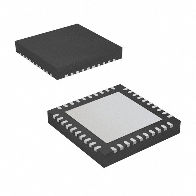
40-Pin MLF
CLKC7
CLKT7
VDDQ
FB_INT
FB_INC
FB_OUTC
FB_OUTT
VDDQ
OE
OS
�ICS97ULP877B
Pin Descriptions
Te r m i n a l
Name
Electrical
Characteristics
Description
AGND
Analog Ground
Ground
AVDD
A n a l o g p ow e r
1.8 V nominal
CLK_INT
Clock input with a (10K-100K Ohm) pulldown resistor
Differential input
CLK_INC
Complentar y clock input with a (10K-100K Ohm) pulldown resistor
Differential input
FB_INT
Feedback clock input
Differential input
FB_INC
Complementary feedback clock input
Differential input
FB_OUTT
Feedback clock output
Differential output
FB_OUTC
Complementary feedback clock output
Differential output
OE
Output Enable (Asynchronous)
LVCMOS input
OS
Output Select (tied to GND or VDDQ)
LVCMOS input
GND
Ground
Ground
VDDQ
Logic and output power
1.8V nominal
CLKT[0:9]
Clock outputs
Differential outputs
CLKC[0:9]
Complementary clock outputs
Differential outputs
NB
No ball
The PLL clock buffer, ICS97ULP877B, is designed for a VDDQ of 1.8 V, a AVDD of 1.8 V and differential data input and
output levels. Package options include a plastic 52-ball VFBGA and a 40-pin MLF.
ICS97ULP877B is a zero delay buffer that distributes a differential clock input pair (CLK_INT, CLK_INC) to ten
differential pair of clock outputs (CLKT[0:9], CLKC[0:9]) and one differential pair feedback clock outputs (FB_OUTT,
FBOUTC). The clock outputs are controlled by the input clocks (CLK_INT, CLK_INC), the feedback clocks (FB_INT,
FB_INC), the LVCMOS program pins (OE, OS) and the Analog Power input (AVDD). When OE is low, the outputs (except
FB_OUTT/FB_OUTC) are disabled while the internal PLL continues to maintain its locked-in frequency. OS (Output
Select) is a program pin that must be tied to GND or VDDQ. When OS is high, OE will function as described above. When
OS is low, OE has no effect on CLKT7/CLKC7 (they are free running in addition to FB_OUTT/FB_OUTC). When AVDD
is grounded, the PLL is turned off and bypassed for test purposes.
When both clock signals (CLK_INT, CLK_INC) are logic low, the device will enter a low power mode. An input logic
detection circuit on the differential inputs, independent from the input buffers, will detect the logic low level and perform
a low power state where all outputs, the feedback and the PLL are OFF. When the inputs transition from both being logic
low to being differential signals, the PLL will be turned back on, the inputs and outputs will be enabled and the PLL
will obtain phase lock between the feedback clock pair (FB_INT, FB_INC) and the input clock pair (CLK_INT, CLK_INC)
within the specified stabilization time tSTAB.
The PLL in ICS97ULP877B clock driver uses the input clocks (CLK_INT, CLK_INC) and the feedback clocks (FB_INT,
FB_INC) to provide high-performance, low-skew, low-jitter output differential clocks (CLKT[0:9], CLKC[0:9]).
ICS97ULP877B is also able to track Spread Spectrum Clocking (SSC) for reduced EMI.
ICS97ULP877B is characterized for operation from 0°C to 70°C.
0981C—04/05/05
2
�ICS97ULP877B
Function Table
Inputs
Outputs
PLL
AVDD
OE
OS
CLK_INT
CLK_INT
CLKT
CLKC
FB_OUTT
FB_OUTC
GND
H
X
L
H
L
H
L
H
Bypassed/Off
GND
H
X
H
L
H
L
H
L
Bypassed/Off
GND
L
H
L
H
*L(Z)
*L(Z)
L
H
Bypassed/Off
GND
L
L
H
L
*L(Z),
CLKT7
active
*L(Z),
CLKC7
active
H
L
Bypassed/Off
1.8V(nom)
L
H
L
H
*L(Z)
*L(Z)
L
H
On
1.8V(nom)
L
L
H
L
*L(Z),
CLKT7
active
*L(Z),
CLKC7
active
H
L
On
1.8V(nom)
H
X
L
H
L
H
L
H
On
1.8V(nom)
H
X
H
L
H
L
H
L
On
1.8V(nom)
X
X
L
L
*L(Z)
*L(Z)
*L(Z)
*L(Z)
Off
1.8V(nom)
X
X
H
H
Reser ved
*L(Z) means the outputs are disabled to a low stated meeting the IODL limit.
0981C—04/05/05
3
�ICS97ULP877B
Absolute Maximum Ratings
Supply Voltage (VDDQ & AVDD) . . . . . . . . .
Logic Inputs . . . . . . . . . . . . . . . . . . . . . . . . .
Ambient Operating Temperature . . . . . . . . . .
Storage Temperature . . . . . . . . . . . . . . . . . . .
-0.5V to 2.5V
GND - 0.5V to VDDQ + 0.5V
0°C to +70°C
-65°C to +150°C
Stresses above those listed under Absolute Maximum Ratings may cause permanent damage to the device. These
ratings are stress specifications only and functional operation of the device at these or any other conditions above those
listed in the operational sections of the specifications is not implied. Exposure to absolute maximum rating conditions
for extended periods may affect product reliability.
Electrical Characteristics - Input/Supply/Common Output Parameters
TA = 0 - 70°C; Supply Voltage AVDDQ, VDDQ = 1.8 V +/- 0.1V (unless otherwise stated)
PARAMETER
SYMBOL
CONDITIONS
MIN
TYP
Input High Current
V I = VDDQ or GND
IIH
(CLK_INT, CLK_INC)
Input Low Current (OE,
V I = VDDQ or GND
IIL
OS, FB_INT, FB_INC)
Output Disabled Low
OE = L, V ODL = 100mV
100
IODL
Current
IDD1.8 CL = 0pf @ 270MHz
Operating Supply
Current
IDDLD
CL = 0pf
Input Clamp Voltage
VIK
V DDQ = 1.7V Iin = -18mA
High-level output
I OH = -100 A
VDDQ - 0.2
VOH
voltage
I OH = -9 mA
1.1
1.45
I OL=100 A
0.25
Low-level output voltage
VOL
I OL=9 mA
CIN
V I = GND or V DDQ
2
Input Capacitance1
1
COUT
V OUT = GND or VDDQ
2
Output Capacitance
1
Guaranteed by design, not 100% tested in production.
0981C—04/05/05
4
MAX
UNITS
±250
µA
±10
µA
µA
200
500
-1.2
0.10
0.6
3
3
mA
µA
V
V
V
V
V
pF
pF
�ICS97ULP877B
Recommended Operating Condition (see note1)
TA = 0 - 70°C; Supply Voltage AVDD, VDDQ = 1.8 V +/- 0.1V (unless otherwise stated)
PARAMETER
Supply Voltage
Low level input voltage
High level input voltage
DC input signal voltage
(note 2)
Differential input signal
voltage (note 3)
Output differential crossvoltage (note 4)
Input differential crossvoltage (note 4)
High level output current
Low level output current
Operating free-air
temperature
SYMBOL
V DDQ, AVDD
V IL
VIH
CONDITIONS
MIN
1.7
CLK_INT, CLK_INC, FB_INC,
FB_INT
OE, OS
CLK_INT, CLK_INC, FB_INC,
0.65 x VDDQ
FB_INT
OE, OS
0.65 x VDDQ
VIN
TYP
1.8
MAX
1.9
UNITS
V
0.35 x V DDQ
V
0.35 x V DDQ
V
V
V
-0.3
V DDQ + 0.3
V
0.3
V DDQ + 0.4
V
0.6
V DDQ + 0.4
V
VOX
VDDQ/2 - 0.10
V DDQ/2 + 0.10
V
VIX
VDDQ/2 - 0.15 VDD/2 V DDQ2 + 0.15
V
VID
DC - CLK_INT, CLK_INC,
FB_INC, FB_INT
AC - CLK_INT, CLK_INC,
FB_INC, FB_INT
IOH
IOL
TA
0
Notes:
1. Unused inputs must be held high or low to prevent them from floating.
2. DC input signal voltage specifies the allowable DC execution of differential input.
3. Differential inputs signal voltages specifies the differential voltage [VTR-VCP]
required for switching, where VTR is the true input level and VCP is the
complementary input level.
4. Differential cross-point voltage is expected to track variations of VDDQ and is the
voltage at which the differential signal must be crossing.
0981C—04/05/05
5
-9
9
mA
mA
70
°C
�ICS97ULP877B
Timing Requirements
T A = 0 - 70°C Supply Voltage AVDD, VDDQ = 1.8 V + /- 0.1V (unless otherwise stated)
CONDITIONS
PARAMETER
SYMBOL
MIN
MAX
UNITS
Max clock frequency
freqop
1.8V+0.1V @ 25°C
95
410
MHz
Application Frequency
Range
freqApp
1.8V+0.1V @ 25°C
160
410
MHz
Input clock duty cycle
dtin
40
60
%
15
µs
CLK stabilization
T STAB
NOTE: The PLL must be able to handle spread spectrum induced skew.
NOTE: Operating clock frequency indicates a range over which the PLL must be able to lock, but in which it is not
required to meet the other timing parameters. (Used for low speed system debug.)
NOTE: Application clock frequency indicates a range over which the PLL must meet all timing parameters.
NOTE: Stabilization time is the time required for the integrated PLL circuit to obtain phase lock of its feedback
signal to its reference signal, within the value specificied by the Static Phase Offset (t(Æ ), after power-up. During
normal operation, the stabilization time is also the time required for the integrated PLL circuit to obtain phase lock
of its feedback signal to its reference signal when CK and CK go to a logic low state, enter the power-down mode
and later return to active operation. CK and CK may be left floating after they have been driven low for one
complete clock cycle.
0981C—04/05/05
6
�ICS97ULP877B
Switching Characteristics1
TA = 0 - 70°C Supply Voltage AVDD, VDDQ = 1.8 V +/- 0.1V (unless otherwise stated)
PARAMETER
CONDITION
(MHz)
SYMBOL
ten
Output enable time
OE to any output
160 to 410
tdis
OE to any output
Output disable time
160 to 270
tjit (per)
Period jitter
271 to 410
160 to 270
tjit(hper)
Half-period jitter
271 to 410
Input Clock
Input slew rate
SLr1(i)
Output Enable (OE), (OS)
Output clock slew rate
160 to 410
SLr1(o)
tjit(cc+)
Cycle-to-cycle period jitter
tjit(cc-)
160 to 270
t(Ø)dyn
Dynamic Phase Offset
271 to 410
2
Static Phase Offset
271 to 410
tSPO
∑(su)
t jit (per) + t (Ø)dyn + t skew(o)
t(Ø)dyn + tskew(o)
∑t (h)
160 to 270
tskew
Output to Output Skew
271 to 410
SSC modulation frequency
SSC clock input frequency
deviation
PLL Loop bandwidth (-3 dB
from unity gain)
Notes:
1. Switching characteristics guaranteed for application frequency range.
2. Static phase offset shifted by design.
0981C—04/05/05
7
MIN
30.00
3
40
-40
50
20
50
80
60
40
30
33
UNITS
ns
ns
ps
ps
ps
ps
v/ns
v/ns
v/ns
ps
ps
ps
ps
ps
ps
ps
ps
ps
kHz
0.00
-0.50
%
-40
-30
-60
-50
1
0.5
1.5
0
0
-50
-20
-50
2.0
TYP
4.73
5.82
2.5
2.5
0
MAX
8
8
40
30
60
50
4
MHz
�ICS97ULP877B
Parameter Measurement Information
VDD
V(CLKC)
V(CLKC)
ICS97ULP877B
GND
Figure 1. IBIS Model Output Load
VDD/2
C = 10 pF - GND
ICS97ULP877B
R = 10Ω
Z = 60Ω
SCOPE
Z = 50Ω
Z = 2.97"
R = 1MΩ
V(TT) C = 1 pF
Z = 120Ω
R = 10Ω
Z = 60Ω
Z = 50Ω
Z = 2.97"
R = 1MΩ
V(TT) C = 1 pF
C = 10 pF
Note: VTT = GND
GND
-VDD/2
Figure 2. Output Load Test Circuit
YX, FB_OUTC
YX, FB_OUTT
tc(n)
tc(n+1)
tjit(cc) = tc(n) ± tc(n+1)
Figure 3. Cycle-to-Cycle Jitter
0981C—04/05/05
8
�ICS97ULP877B
Parameter Measurement Information
CLK_INC
CLK_INT
FB_INC
FB_INT
t( ) n
n=N
t( ) n
1
t( )=
N
(N is a large number of samples)
Figure 4. Static Phase Offset
YX#
YX
YX, FB_OUTC
YX, FB_OUTT
t(skew)
Figure 5. Output Skew
YX, FB_OUTC
YX, FB_OUTT
tC(n)
YX, FB_OUTC
YX, FB_OUTT
1
fO
t(jit_per) = tc(n) - 1
fO
Figure 6. Period Jitter
0981C—04/05/05
9
t ( ) n+1
�ICS97ULP877B
Parameter Measurement Information
YX, FB_OUTC
YX, FB_OUTT
t jit(hper_n+1)
t jit(hper_n)
1
fo
tjit(hper) = t jit(hper_n)
-
1
2xfO
Figure 7. Half-Period Jitter
80%
80%
VID, VOD
Clock Inputs
and Outputs
20%
20%
tslr
tslf
Figure 8. Input and Output Slew Rates
0981C—04/05/05
10
�ICS97ULP877B
CK
CK
FBIN
FBIN
t(
t(
)
SSC OFF
SSC ON
t(
)
SSC OFF
SSC ON
t(
)dyn
t(
)dyn
t(
)dyn
Figure 9. Dynamic Phase Offset
50% VDDQ
OE
t en
Y
50% VDDQ
Y
Y/ Y
OE
50% VDDQ
t dis
Y
50 % VDDQ
Y
Figure 10. Time delay between OE and Clock Output (Y, Y)
0981C—04/05/05
11
)dyn
�ICS97ULP877B
Figure 11. AVDD Filtering
- Place the 2200pF capacitor close to the PLL.
- Use a wide trace for the PLL analog power & ground. Connect PLL & caps to AGND trace & connect trace to one
GND via (farthest from PLL).
- Recommended bead: Fair-Rite P/N 2506036017Y0 or equivalent (0.8 Ohm DC max, 600 Ohms @ 100 MHz).
0981C—04/05/05
12
�ICS97ULP877B
C
Seating
Plane
A1
Numeric Designations
for Horizontal Grid
b
REF
T
4 3 2 1
A
B
C
D
Alpha Designations
for Vertical Grid
(Letters I, O, Q & S
not used)
D
d TYP
D1
- e - TYP
TOP VIEW
E
c
REF
h
TYP
- e - TYP
E1
0.12 C
ALL DIMENSIONS IN MILLIMETERS
D
E
7.00 Bsc
4.50 Bsc
T
Min/Max
0.86/1.00
----- BALL GRID ----HORIZ
VERT
e
0.65 Bsc
6
10
Max.
TOTAL
60
d
Min/Max
0.35/0.45
h
Min/Max
0.15/0.21
D1
E1
5.85 Bsc
3.25 Bsc
Note: Ball grid total indicates maximum ball count for package. Lesser quantity may be used.
* Source Ref.: JEDEC Publication 95,
MO-205*, MO-225**
10-0055
Ordering Information
ICS97ULP877BHLF-T
Example:
ICS XXXX y H LF- T
Designation for tape and reel packaging
Annealed Lead Free (Optional)
Package Type
H = BGA
Revision Designator (will not correlate with datasheet revision)
Device Type
Prefix
ICS = Standard Device
0981C—04/05/05
13
REF. DIMENSIONS
b
c
0.575
0.625
**
�ICS97ULP877B
(Ref.)
Seating Plane
(N D -1)x e
(Ref.)
A1
Index Area
ND & NE
Even
A3
N
L
N
1
Anvil
Singulation
1
2
Top View
(NE -1)x e
(Ref.)
E2
2
Sawn
Singulation
b
(Ref.)
A
D
are Even
2
E2
or
E
(Typ.)
e
2 If N & N
D
E
e
ND & NE
Odd
D2
2
Thermal
Base
D2
0.08
C
C
THERMALLY ENHANCED, VERY THIN, FINE PITCH
QUAD FLAT / NO LEAD PLASTIC PACKAGE
ALL D IMENSIONS IN MILLIMETERS
N
ND
NE
D x E BASIC
D2 M IN. / MAX.
E2 M IN. / MAX.
L MIN. / MAX.
40
10
10
6.00 x 6.00
2.75 / 3.05
2.75 / 3.05
0.30 / 0.50
SY MBOL
A
A1
A3
b
e
MIN.
M AX.
0.80
1.00
0
0.05
0.25 Reference
0.18
0.30
0.50 BASIC
Source R eference: MLF2™SE
10-0053
Ordering Information
ICS97ULP877BKLF-T
Example:
ICS XXXX y K LF- T
Designation for tape and reel packaging
Annealed Lead Free (Optional)
Package Type
K = MLF
Revision Designator (will not correlate with datasheet revision)
Device Type
Prefix
ICS = Standard Device
0981C—04/05/05
14
�IMPORTANT NOTICE AND DISCLAIMER
RENESAS ELECTRONICS CORPORATION AND ITS SUBSIDIARIES (“RENESAS”) PROVIDES TECHNICAL
SPECIFICATIONS AND RELIABILITY DATA (INCLUDING DATASHEETS), DESIGN RESOURCES (INCLUDING
REFERENCE DESIGNS), APPLICATION OR OTHER DESIGN ADVICE, WEB TOOLS, SAFETY INFORMATION, AND
OTHER RESOURCES “AS IS” AND WITH ALL FAULTS, AND DISCLAIMS ALL WARRANTIES, EXPRESS OR IMPLIED,
INCLUDING, WITHOUT LIMITATION, ANY IMPLIED WARRANTIES OF MERCHANTABILITY, FITNESS FOR A
PARTICULAR PURPOSE, OR NON-INFRINGEMENT OF THIRD PARTY INTELLECTUAL PROPERTY RIGHTS.
These resources are intended for developers skilled in the art designing with Renesas products. You are solely responsible
for (1) selecting the appropriate products for your application, (2) designing, validating, and testing your application, and (3)
ensuring your application meets applicable standards, and any other safety, security, or other requirements. These
resources are subject to change without notice. Renesas grants you permission to use these resources only for
development of an application that uses Renesas products. Other reproduction or use of these resources is strictly
prohibited. No license is granted to any other Renesas intellectual property or to any third party intellectual property.
Renesas disclaims responsibility for, and you will fully indemnify Renesas and its representatives against, any claims,
damages, costs, losses, or liabilities arising out of your use of these resources. Renesas' products are provided only subject
to Renesas' Terms and Conditions of Sale or other applicable terms agreed to in writing. No use of any Renesas resources
expands or otherwise alters any applicable warranties or warranty disclaimers for these products.
(Rev.1.0 Mar 2020)
Corporate Headquarters
Contact Information
TOYOSU FORESIA, 3-2-24 Toyosu,
Koto-ku, Tokyo 135-0061, Japan
www.renesas.com
For further information on a product, technology, the most
up-to-date version of a document, or your nearest sales
office, please visit:
www.renesas.com/contact/
Trademarks
Renesas and the Renesas logo are trademarks of Renesas
Electronics Corporation. All trademarks and registered
trademarks are the property of their respective owners.
© 2020 Renesas Electronics Corporation. All rights reserved.
�


 工商网监
湘ICP备2023018690号
工商网监
湘ICP备2023018690号
