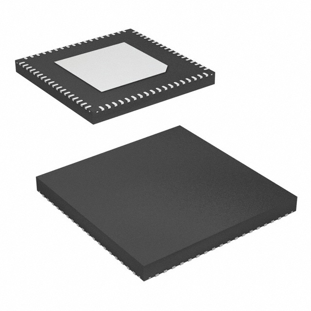
ICS9FG1901
Integrated
Circuit
Systems, Inc.
Frequency Generator for P4™ CPU, PCI Express™ & Fully Buffered DIMM Clocks
Functionality at Power Up (PLL Mode)
Recommended Application:
DB1900G: CPU Host Bus, PCI Express and Fully-Buffered
DIMM clocking
FS_A_4101
1
0
Features:
Power Down Functionality
INPUTS
OUTPUTS
PLL State
VDDA/PD# CLK_IN/CLK_IN# DIF DIF#
Running
3.3V (NOM)
Running
ON
Hi-Z
GND
X
OFF
Functionality Note
It is recommended that Byte 2, bit 6 be toggled from 1 to 0
and back to 1, the first time VDDA is applied. This ensures
proper initialization of the device.
Key Specifications:
DIF output cycle-to-cycle jitter < 50ps
DIF (0:18) output-to-output skew < 225ps
DIF (0:16) output-to-output skew < 100ps
DIF_14
DIF_14#
OE15#
DIF_15
DIF_15#
OE16#
GND
DIF_17
DIF_17#
DIF_18
DIF_18#
OE17_18#
CLK_IN
Pin Configuration
CLK_IN#
SMB_A2_PLLBYP#
•
•
•
DIF_16
•
•
•
•
•
DIF_(18:0)
MHz
CLK_IN
CLK_IN
1. FS_A_410 is a low-threshold input. Please see the VIL_FS and VIH_FS
specifications in the Input/Supply/Common Output Parameters Table for
correct values.
DIF_16#
•
Power up default is all outputs in 1:1 mode
DIF_(16:0) can be “gear-shifted” from the input CPU
Host Clock
DIF_(18:17) can be “gear-shifted” from the input CPU
Host Clock
Spread spectrum compatible
Supports output clock frequencies up to 400 MHz
8 Selectable SMBus addresses
SMBus address determines PLL or Bypass mode
VDDA controlled power down mode
VDD
•
•
CLK_IN (CPU FSB)
MHz
100
很抱歉,暂时无法提供与“ICS9FG1901CKLFT”相匹配的价格&库存,您可以联系我们找货
免费人工找货