DATASHEET
ISL28133
FN6560
Rev.7.1
Apr 22, 2021
Single Micropower, Chopper Stabilized, RRIO Operational Amplifier
The ISL28133 is a single micropower, chopper stabilized
operational amplifier that is optimized for single supply
operation from 1.8V to 5.5V. Its low supply current of 18µA
and wide input range enable make it an excellent general
purpose op amp for a range of applications. The ISL28133 is
ideal for handheld devices that operate off 2 AA or single Li-ion
batteries.
Features
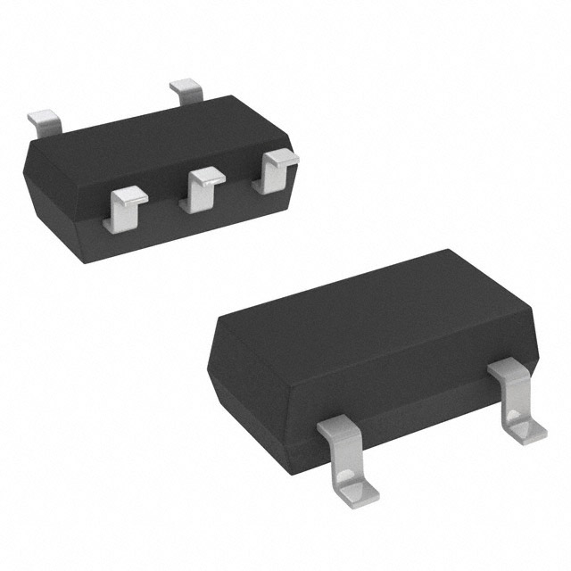
The ISL28133 is available in the 5 Ld SOT-23 and 5 Ld SC70
packages. All devices operate over the extended temperature
range of -40°C to +125°C.
• Wide supply range . . . . . . . . . . . . . . . . . . . . . . . . . 1.8V to 5.5V
• Low input offset voltage . . . . . . . . . . . . . . . . . . . . . . 8µV, Max.
• Low offset TC . . . . . . . . . . . . . . . . . . . . . . . . 0.075µV/°C, Max
• Input bias current. . . . . . . . . . . . . . . . . . . . . . . . . . 300pA, Max.
• Quiescent current . . . . . . . . . . . . . . . . . . . . . . . . . . .18µA, Typ.
• Low noise (0.01Hz to 10Hz) . . . . . . . . . . . . . . . . .1.1µVP-P, Typ.
• Rail-to-rail inputs and output
• Operating temperature range. . . . . . . . . . . .-40°C to +125°C
Applications
• Bidirectional current sense
• Temperature measurement
• Medical equipment
• Electronic weigh scales
10
VS
1.8V TO +5.5V
I-SENSE+
VREF
0.1
4.99k
499k
5
+ V+
1
ISL28133
4
V2
499k
3
VSENSE
OUT
MAX
6
VOS (µV)
4.99k
N = 67
8
4
MEDIAN
2
0
-2
MIN
-4
-6
GND
I-SENSE-
-40
-20
0
20
40
60
80
100
120
TEMPERATURE (°C)
BIDIRECTIONAL CURRENT SENSE AMPLIFIER
FIGURE 1. TYPICAL APPLICATION CIRCUIT
FN6560 Rev.7.1
Apr 22, 2021
FIGURE 2. VOS vs TEMPERATURE
Page 1 of 19
© 2009 Renesas Electronics
�ISL28133
Block Diagram
V+
MAIN AMPLIFIER
+
5kHz CROSSOVER
FILTER
-
IN+
VOUT
+
INCLOCK GEN + DRIVERS
V-
Ordering Information
PART NUMBER
ISL28133FHZ-T7 (Note 2)
PART MARKING
BCFA (Note 5)
PACKAGE DESCRIPTION
(RoHS Compliant)
5 Ld SOT-23
PKG.
DWG. #
CARRIER TYPE
(Note 1)
P5.064A
Reel, 3k
ISL28133FHZ-T7A (Note 2)
Reel, 250
ISL28133FEZ-T7 (Note 2)
BHA (Note 5)
ISL28133ISENSEV1Z
Evaluation Board
ISL28133EVAL1Z
Evaluation Board
ISL28133CSENSEV1Z
Evaluation Board
5 Ld SC70
P5.049
Reel, 3k
NOTES:
1. See TB347 for details on reel specifications.
2. These Pb-free plastic packaged products employ special Pb-free material sets, molding compounds/die attach materials, and 100% matte tin plate plus
anneal (e3 termination finish, which is RoHS compliant and compatible with both SnPb and Pb-free soldering operations). Pb-free products are MSL
classified at Pb-free peak reflow temperatures that meet or exceed the Pb-free requirements of IPC/JEDEC J STD-020.
3. These Pb-free plastic packaged products employ special Pb-free material sets; molding compounds/die attach materials and NiPdAu plate - e4 termination
finish, which is RoHS compliant and compatible with both SnPb and Pb-free soldering operations. Pb-free products are MSL classified at Pb-free peak reflow
temperatures that meet or exceed the Pb-free requirements of IPC/JEDEC J STD-020.
4. For Moisture Sensitivity Level (MSL), please see the device information page for the ISL28133. For more information on MSL please see techbrief
TB363.
5. The part marking is located on the bottom of the part.
FN6560 Rev.7.1
Apr 22, 2021
Page 2 of 19
�ISL28133
Pin Configurations
1
V-
2
IN+
3
5
V+
IN+
1
V-
2
IN-
3
+ 4
IN-
5
V+
+
OUT
ISL28133
(5 LD SC-70)
TOP VIEW
-
ISL28133
(5 LD SOT-23)
TOP VIEW
4
OUT
TOP VIEW
Pin Descriptions
ISL28133
(5 Ld SOT23)
ISL28133
(5 Ld SC-70)
PIN
NAME
3
1
IN+
FUNCTION
EQUIVALENT CIRCUIT
Non-inverting input
V+
+
-
IN+
+
IN-
CLOCK GEN + DRIVERS
VCircuit 1
2
2
V-
Negative supply
4
3
IN-
Inverting input
1
4
OUT
Output
(See Circuit 1)
V+
OUT
VCircuit 2
5
FN6560 Rev.7.1
Apr 22, 2021
5
V+
Positive supply
Page 3 of 19
�ISL28133
Absolute Maximum Ratings
Thermal Information
Max Supply Voltage V+ to V- . . . . . . . . . . . . . . . . . . . . . . . . . . . . . . . . . . .6.5V
Max Voltage VIN to GND . . . . . . . . . . . . . . . . . . . . . . . . . . . . . . -0.5V to 6.5V
Max Input Differential Voltage . . . . . . . . . . . . . . . . . . . . . . . . . . . . . . . . 6.5V
Max Input Current . . . . . . . . . . . . . . . . . . . . . . . . . . . . . . . . . . . . . . . . . 20mA
Max Voltage VOUT to GND (10s) . . . . . . . . . . . . . . . . . . . . . . . . . . . . . . . .6.5V
ESD Rating
Human Body Model . . . . . . . . . . . . . . . . . . . . . . . . . . . . . . . . . . . . . . 3000V
Machine Model . . . . . . . . . . . . . . . . . . . . . . . . . . . . . . . . . . . . . . . . . . . 200V
Charged Device Model . . . . . . . . . . . . . . . . . . . . . . . . . . . . . . . . . . . . 1500V
Thermal Resistance (Typical)
JA (°C/W) JC (°C/W)
5 Ld SOT-23 (Note 6, 7) . . . . . . . . . . . . . . . .
225
110
5 Ld SC-70 (Note 6) . . . . . . . . . . . . . . . . . . .
206
N/A
Maximum Storage Temperature Range . . . . . . . . . . . .-65°C to +150°C
Pb-Free Reflow Profile . . . . . . . . . . . . . . . . . . . . . . . . . . . . . . . . . . see TB493
Operating Conditions
Temperature Range . . . . . . . . . . . . . . . . . . . . . . . . . . . . . . .-40°C to +125°C
Maximum Junction Temperature . . . . . . . . . . . . . . . . . . . . . . . . . . . . . 140°C
CAUTION: Do not operate at or near the maximum ratings listed for extended periods of time. Exposure to such conditions may adversely impact product
reliability and result in failures not covered by warranty.
NOTES:
6. JA is measured with the component mounted on a high effective thermal conductivity test board in free air. See TB379 for details.
7. For JC, the “case temp” location is taken at the package top center.
Electrical Specifications V+ = 5V, V- = 0V, VCM = 2.5V, TA = +25°C, RL = Open, unless otherwise specified. Boldface limits apply
over the operating temperature range, -40°C to +125°C.
PARAMETER
DESCRIPTION
CONDITIONS
MIN
(Note 8)
TYP
MAX
(Note 8)
UNIT
-8
±2
8
µV
15.5
µV
0.075
µV/°C
DC SPECIFICATIONS
VOS
Input Offset Voltage
-15.5
TCVOS
Input Offset Voltage Temperature
Coefficient
0.02
IOS
Input Offset Current
-60
IB
Input Bias Current
Common Mode Input
Voltage Range
CMRR
Common Mode Rejection Ratio
-300
±30
pA
300
pA
-600
600
pA
V+ = 5.0V, V- = GND
-0.1
5.1
V
VCM = -0.1V to 5.0V
118
125
dB
115
PSRR
Power Supply Rejection Ratio
Vs = 2V to 5.5V
110
dB
138
dB
110
VOH
Output Voltage Swing, High
RL = 10k
VOL
Output Voltage Swing, Low
RL = 10k
18
AOL
Open Loop Gain
RL = 1M
174
V+
Supply Voltage
(Note 9)
IS
Supply Current
RL = OPEN
ISC+
Output Source Short Circuit Current
ISC-
Output Sink Short Circuit Current
RL = Short to ground or V+
4.965
dB
4.981
1.8
18
V
35
mV
dB
5.5
V
25
µA
35
µA
13
17
26
mA
-26
-19
-13
mA
AC SPECIFICATIONS
GBWP
Gain Bandwidth Product
f = 50kHz
AV = 100, RF = 100k
RG = 1kRL = 10kto VCM
400
kHz
eN VP-P
Peak-to-Peak Input Noise Voltage
f = 0.01Hz to 10Hz
1.1
µVP-P
eN
Input Noise Voltage Density
f = 1kHz
65
nV/(Hz)
FN6560 Rev.7.1
Apr 22, 2021
Page 4 of 19
�ISL28133
Electrical Specifications V+ = 5V, V- = 0V, VCM = 2.5V, TA = +25°C, RL = Open, unless otherwise specified. Boldface limits apply
over the operating temperature range, -40°C to +125°C. (Continued)
PARAMETER
iN
DESCRIPTION
Input Noise Current Density
Differential Input Capacitance
Cin
MIN
(Note 8)
CONDITIONS
MAX
(Note 8)
TYP
UNIT
f = 1kHz
72
fA/(Hz)
f = 10Hz
79
fA/(Hz)
f = 1MHz
1.6
pF
1.12
pF
0.2
V/µs
0.1
V/µs
1.1
µs
1.1
µs
8
µs
10
µs
35
µs
Common Mode Input Capacitance
TRANSIENT RESPONSE
SR
VOUT = 1V to 4V, RL = 10k
Positive Slew Rate
Negative Slew Rate
tr, tf, Small Signal
AV = +1, VOUT = 0.1VP-P RF = 0
RL = 10kCL = 1.2pF
Rise Time, tr 10% to 90%
Fall Time, tf 10% to 90%
tr, tf Large Signal
AV = +1, VOUT = 2VP-P RF = 0
RL = 10kCL = 1.2pF
Rise Time, tr 10% to 90%
Fall Time, tf 10% to 90%
ts
Settling Time to 0.1%, 2VP-P Step
AV = +1, RF = 0RL = 10k
CL = 1.2pF
NOTES:
8. Compliance to datasheet limits is assured by one or more methods: production test, characterization and/or design.
9. Parts are 100% tested with a minimum operating voltage of 1.8V to a VOS limit of ±15µV.
Typical Performance Curves
V+ = 5V, V- = 0V, VCM = 2.5V, RL = Open.
8
3.5
N = 67
4
2.5
+25°C
2.0
125°C
1.5
MAX
2
-40°C
VOS (µV)
AVERAGE VOS (µV)
3.0
0
MEDIAN
-2
-4
MIN
-6
-8
1.0
0.5
N = 67
6
-10
2.0
2.5
3.0
3.5
4.0
4.5
5.0
5.5
SUPPLY VOLTAGE (V)
FIGURE 3. AVERAGE INPUT OFFSET VOLTAGE vs SUPPLY VOLTAGE
FN6560 Rev.7.1
Apr 22, 2021
-12
-40
-20
0
20
40
60
80
100
120
TEMPERATURE (°C)
FIGURE 4. VOS vs TEMPERATURE, VS = ±1.0V, VIN = 0V, RL = INF
Page 5 of 19
�ISL28133
Typical Performance Curves
V+ = 5V, V- = 0V, VCM = 2.5V, RL = Open. (Continued)
10
200
N = 67
8
6
+125°C
MAX
IBIAS IN+(pA)
VOS (µV)
N = 12
150
4
2
MEDIAN
0
100
50
+100°C
-2
+75°C
0
-4
-6
MIN
-40
-20
-40°C
0
20
40
60
80
100
-50
1.5
120
2.0
+25°C
2.5
TEMPERATURE (°C)
4.5
5.0
5.5
10
N = 12
200
+125°C
+100°C
+75°C
50
+25°C
0
2.5
3.0
3.5
4.0
4.5
-20
-30
-40°C
-40
-50
+125°C
-60
-70
-40°C
2.0
N = 67
-10
AVERAGE IOS (pA)
100
-50
1.5
+25°C
0
150
IBIAS IN- (pA)
4.0
FIGURE 6. IB+ vs SUPPLY VOLTAGE vs TEMPERATURE
250
5.0
-80
1.5
5.5
2.0
2.5
3.0
3.5
4.0
4.5
5.0
5.5
SUPPLY VOLTAGE (V)
SUPPLY VOLTAGE (V)
FIGURE 7. IB- vs SUPPLY VOLTAGE vs TEMPERATURE
FIGURE 8. IOS vs SUPPLY VOLTAGE vs TEMPERATURE
28
25
N = 67
24
N = 67
MAX
26
SUPPLY CURRENT (µA)
AVERAGE SUPPLY CURRENT (µA)
3.5
SUPPLY VOLTAGE (V)
FIGURE 5. VOS vs TEMPERATURE, VS = ±2.5V, VIN = 0V, RL = INF
23
22
+125°C
21
+25°C
20
19
18
24
22
MEDIAN
20
18
MIN
16
17
16
3.0
-40°C
2.0
2.5
3.0
3.5
4.0
4.5
5.0
5.5
SUPPLY VOLTAGE (V)
FIGURE 9. AVERAGE SUPPLY CURRENT vs SUPPLY VOLTAGE
FN6560 Rev.7.1
Apr 22, 2021
14
-40
-20
0
20
40
60
80
100
120
TEMPERATURE (°C)
FIGURE 10. MIN/MAX SUPPLY CURRENT vs TEMPERATURE,
VS = ±0.8V, VIN = 0V, RL = INF
Page 6 of 19
�ISL28133
Typical Performance Curves
30
V+ = 5V, V- = 0V, VCM = 2.5V, RL = Open. (Continued)
800
N = 67
INPUT NOISE VOLTAGE (nV)
SUPPLY CURRENT (µA)
28
MAX
26
24
22
MEDIAN
20
18
16
600
400
200
0
V+ = 5V
RL = 100k
CL = 3.7pF
Rg = 10, Rf = 100k
AV = 10,000
10
20
30
40
-200
-400
MIN
14
-40
-20
0
20
40
60
80
100
-600
120
0
TEMPERATURE (°C)
70
80
90
100
1.0
V+ = 5V
AV = 1
INPUT NOISE CURRENT (pA/ÖHz)
INPUT NOISE VOLTAGE (nV/ÖHz)
1000
100
10
0.001
0.01
0.1
1
10
100
1k
10k
V+ = 5V
AV = 1
0.1
0.01
0.001
100k
0.01
0.1
1
10
100
1k
10k
100k
FREQUENCY (Hz)
FREQUENCY (Hz)
FIGURE 14. INPUT NOISE CURRENT DENSITY vs FREQUENCY
FIGURE 13. INPUT NOISE VOLTAGE DENSITY vs FREQUENCY
200
OPEN LOOP GAIN (dB)/PHASE (°)
200
OPEN LOOP GAIN (dB)/PHASE (°)
60
FIGURE 12. INPUT NOISE VOLTAGE 0.01Hz TO 10Hz
FIGURE 11. MIN/MAX SUPPLY CURRENT vs TEMPERATURE,
VS = ±2.5V, VIN = 0V, RL = INF
150
PHASE
100
50
GAIN
0
-50
50
TIME (s)
RL = 10k
CL = 100pF
SIMULATION
-100
0.1m 1m 10m 100m 1
10 100 1k 10k 100k 1M
FREQUENCY (Hz)
10M
FIGURE 15. FREQUENCY RESPONSE vs OPEN LOOP GAIN, RL = 10k
FN6560 Rev.7.1
Apr 22, 2021
150
PHASE
100
50
GAIN
0
-50
RL = 10M
CL = 100pF
SIMULATION
-100
0.1m 1m 10m 100m 1
10 100 1k 10k 100k 1M
FREQUENCY (Hz)
10M
FIGURE 16. FREQUENCY RESPONSE vs OPEN LOOP GAIN, RL = 10M
Page 7 of 19
�ISL28133
Typical Performance Curves
V+ = 5V, V- = 0V, VCM = 2.5V, RL = Open. (Continued)
2
2
1
0
NORMALIZED GAIN (dB)
NORMALIZED GAIN (dB)
RL = OPEN
RL = 100k
1
RL = 1k
-1
RL = 10k
-2
RL = 49.9k
-3
-4
V+ = 1.6V
-5
CL = 3.7pF
AV = +1
VOUT = 10mVP-P
-6
-7
-8
100
1k
RL = OPEN
0
-1
RL = 1k
-2
RL = 10k
-3
RL = 49.9k
-4
V+ = 5V
CL = 3.7pF
AV = +1
VOUT = 10mVP-P
-5
-6
-7
10k
100k
1M
-8
100
10M
RL = 100k
1k
10k
FREQUENCY (Hz)
FIGURE 17. GAIN vs FREQUENCY vs RL, VS = 1.6V
0
7
NORMALIZED GAIN (dB)
NORMALIZED GAIN (dB)
Rf = Rg = 1k
8
Rf = Rg = 100k
6
5
V+ = 5V
RL = 100k
CL = 3.7pF
AV = +2
VOUT = 10mVP-P
4
3
2
1
0
100
1k
Rf = Rg = 10k
10k
FREQUENCY (Hz)
100k
VOUT = 1V
-3
VOUT = 500mV
-4
-5
-6
V+ = 5V
RL = OPEN
CL = 3.7pF
AV = +1
-7
VOUT = 250mV
1k
VOUT = 100mV
10k
100k
1M
10M
FREQUENCY (Hz)
FIGURE 20. GAIN vs FREQUENCY vs VOUT, RL = OPEN
1
AV = 1000
Rg = 100, Rf = 100k
NORMALIZED GAIN (dB)
0
50
GAIN (dB)
-2
-9
100
1M
70
Rg = 1k, Rf = 100k
AV = 100
V+ = 5V
CL = 3.7pF
RL = 100k
VOUT = 10mVP-P
30
AV = 10
Rg = 10k, Rf = 100k
10
0
VOUT = 10mV
-1
-8
FIGURE 19. GAIN vs FREQUENCY vs FEEDBACK RESISTOR
VALUES Rf/Rg
20
10M
1
9
40
1M
FIGURE 18. GAIN vs FREQUENCY vs RL, VS = 5V
10
60
100k
FREQUENCY (Hz)
AV = 1
-10
10
1k
10k
100k
FREQUENCY (Hz)
1M
10M
FIGURE 21. FREQUENCY RESPONSE vs CLOSED LOOP GAIN
FN6560 Rev.7.1
Apr 22, 2021
-2
V+ = 1.2V
-3
-4
V+ = 3.0V
-5
-6
-7
-8
Rg = OPEN, Rf = 0
100
-1
RL = 100k
CL = 3.7pF
AV = +1
V+ = 1.6V
V+ = 5.5V
VOUT = 10mVP-P
-9
100
1k
10k
100k
1M
10M
FREQUENCY (Hz)
FIGURE 22. GAIN vs FREQUENCY vs SUPPLY VOLTAGE
Page 8 of 19
�ISL28133
Typical Performance Curves
8
10
CL = 824pF
6
0
CL = 474pF
4
-10
-20
CL = 224pF
2
CMRR (dB)
NORMALIZED GAIN (dB)
V+ = 5V, V- = 0V, VCM = 2.5V, RL = Open. (Continued)
0
-2
-4
CL = 104pF
V+ = 5V
-6 RL = 100k
AV = +1
-8 V
OUT = 10mVP-P
-10
100
-40
-50
-80
-90
CL = 3.7pF
10k
100k
FREQUENCY (Hz)
1M
-100
10
10M
10k
100k
0
-20
-10
-20
CMRR (dB)
PSRR+
-40
-50
-60
V+ = 5V
RL = 100k
CL = 16.3pF
AV = +1
VCM = 1VP-P
-70
PSRR-
-80
-90
100
1k
10k
100k
1M
-30
-40
-50
V+ =1.6V
RL = 100k
CL = 16.3pF
AV = +1
VCM = 1VP-P
-60
-70
-80
-90
-100
10
10M
100
1k
10k
100k
FIGURE 25. PSRR vs FREQUENCY, VS = 5V
FIGURE 26. CMRR vs FREQUENCY, VS = 1.6V
200
0
N = 67
-10
180
-20
PSRR+
CMRR (dB)
PSRR (dB)
-40
-50
-60
V+ = 1.6V
RL = 100k
CL = 16.3pF
AV = +1
VCM = 1VP-P
-70
-80
PSRR-
-90
-100
10
10M
1M
FREQUENCY (Hz)
FREQUENCY (Hz)
-30
10M
1M
10
0
PSRR (dB)
1k
FIGURE 24. CMRR vs FREQUENCY, VS = 5V
-10
-100
10
100
FREQUENCY (Hz)
FIGURE 23. GAIN vs FREQUENCY vs CL
-30
V+ = 5V
RL = 100k
CL = 16.3pF
AV = +1
VCM = 1VP-P
-60
-70
CL = 51pF
1k
-30
100
1k
10k
100k
1M
FREQUENCY (Hz)
FIGURE 27. PSRR vs FREQUENCY, VS = 1.6V
FN6560 Rev.7.1
Apr 22, 2021
MAX
MEDIAN
160
140
120
MIN
100
10M
80
-40
-20
0
20
40
60
80
100
120
TEMPERATURE (°C)
FIGURE 28. CMRR vs TEMPERATURE, VCM = -2.5V TO +2.5V,
V+ = ±2.5V
Page 9 of 19
�ISL28133
Typical Performance Curves
V+ = 5V, V- = 0V, VCM = 2.5V, RL = Open. (Continued)
155
5.0
N = 67
145
4.5
MAX
4.0
MEDIAN
125
PSRR (dB)
LARGE SIGNAL (V)
135
115
105
MIN
95
3.5
3.0
V+ = 5V
RL = 100k
CL = 3.7pF
AV = 1
VOUT = 4VP-P
2.5
2.0
1.5
1.0
85
0.5
75
-40
-20
0
20
40
60
80
100
0
120
0
50
100
150
TEMPERATURE (°C)
0.14
1.0
0.12
SMALL SIGNAL (V)
LARGE SIGNAL (V)
1.2
0.8
V+ = 5V
RL = 100k
CL = 3.7pF
AV = 1
VOUT = 1VP-P
0.4
0.2
0
10
20
30
40
50
60
70
80
90
0.06
0
5
10
15
20
25
30
35
40
TIME (µs)
FIGURE 32. SMALL SIGNAL STEP RESPONSE (100mV)
0.024
4.986
N = 67
MAX
MAX
0.022
MEDIAN
MIN
4.976
VOUT (V)
4.980
4.978
N = 67
0.023
4.982
VOUT (V)
400
V+ = 5V
RL = 100k
CL = 3.7pF
AV = 1
VOUT = 100mVP-P
0.04
0
100
FIGURE 31. LARGE SIGNAL STEP RESPONSE (1V)
0.021
0.020
MEDIAN
0.019
0.018
4.974
4.972
-40
350
0.08
TIME (µs)
4.984
300
0.10
0.02
0
250
FIGURE 30. LARGE SIGNAL STEP RESPONSE (4V)
FIGURE 29. PSRR vs TEMPERATURE, V+ = 2V TO 5.5V
0.6
200
TIME (µs)
0.017
-20
0
20
40
60
80
100
120
TEMPERATURE (°C)
FIGURE 33. VOUT HIGH vs TEMPERATURE, RL = 10k, VS = 5V
FN6560 Rev.7.1
Apr 22, 2021
0.016
-40
MIN
-20
0
20
40
60
80
100
120
TEMPERATURE (°C)
FIGURE 34. VOUT LOW vs TEMPERATURE, RL = 10k, VS = 5V
Page 10 of 19
�ISL28133
Typical Performance Curves
V+ = 5V, V- = 0V, VCM = 2.5V, RL = Open. (Continued)
3.0
VOUT (V)
2.0
VOH
1.0
0.0
-1.0
VOL
-2.0
-3.0
0
1
2
3
4
5
6
IOUT (mA)
7
8
9
10
FIGURE 35. VOH, VOL vs IOUT, VS = ±2.5V
n
Applications Information
Functional Description
The ISL28133 uses a proprietary chopper-stabilized architecture
shown in the “Block Diagram” on page 2. The ISL28133
combines a 400kHz main amplifier with a very high open loop
gain (174dB) chopper stabilized amplifier to achieve very low
offset voltage and drift (2µV, 0.02µV/°C typical) while
consuming only 18µA of supply current per channel.
This multi-path amplifier architecture contains a time continuous
main amplifier whose input DC offset is corrected by a
parallel-connected, high gain chopper stabilized DC correction
amplifier operating at 100kHz. From DC to ~5kHz, both
amplifiers are active with DC offset correction and most of the
low frequency gain is provided by the chopper amplifier. A 5kHz
crossover filter cuts off the low frequency amplifier path leaving
the main amplifier active out to the 400kHz gain-bandwidth
product of the device.
IN+ and IN- Protection
All input terminals have internal ESD protection diodes to both
positive and negative supply rails, limiting the input voltage to
within one diode beyond the supply rails. For applications where
either input is expected to exceed the rails by 0.5V, an external
series resistor must be used to ensure the input currents never
exceed 20mA (see Figure 36).
VIN
RIN
+
VOUT
RL
FIGURE 36. INPUT CURRENT LIMITING
Layout Guidelines for High Impedance Inputs
The key benefits of this architecture for precision applications are
very high open loop gain, very low DC offset, and low 1/f noise.
The noise is virtually flat across the frequency range from a few
mHz out to 100kHz, except for the narrow noise peak at the
amplifier crossover frequency (5kHz).
To achieve the maximum performance of the high input
impedance and low offset voltage of the ISL28133 amplifiers,
care should be taken in the circuit board layout. The PC board
surface must remain clean and free of moisture to avoid leakage
currents between adjacent traces. Surface coating of the circuit
board will reduce surface moisture and provide a humidity barrier,
reducing parasitic resistance on the board.
Rail-to-rail Input and Output (RRIO)
High Gain, Precision DC-Coupled Amplifier
The RRIO CMOS amplifier uses parallel input PMOS and NMOS
that enable the inputs to swing 100mV beyond either supply rail.
The inverting and non-inverting inputs do not have back-to-back
input clamp diodes and are capable of maintaining high input
impedance at high differential input voltages. This is effective in
eliminating output distortion caused by high slew-rate input
signals.
The circuit in Figure 37 implements a single-stage, 10kV/V
DC-coupled amplifier with an input DC sensitivity of under 100nV
that is only possible using a low VOS amplifier with high open
loop gain. This circuit is practical down to 1.8V due to it's
rail-to-rail input and output capability. Standard high gain DC
amplifiers operating from low voltage supplies are not practical
at these high gains using typical low offset precision op amps
because the input offset voltage and temperature coefficient
consume most of the available output voltage swing. For
example, a typical precision amplifier in a gain of 10kV/V with a
±100µV VOS and a temperature coefficient of 0.5µV/°C would
produce a DC error at the output of >1V with an additional
5mV°C of temperature dependent error. At 3V, this DC error
The output stage uses common source connected PMOS and
NMOS devices to achieve rail-to-rail output drive capability with
17mA current limit and the capability to swing to within 20mV of
either rail while driving a 10k load.
FN6560 Rev.7.1
Apr 22, 2021
Page 11 of 19
�ISL28133
consumes > 30% of the total supply voltage, making it
impractical to measure sub-microvolt low frequency signals.
The ±8µV max VOS and 0.075µV/°C of the ISL28133 produces a
temperature stable maximum DC output error of only ±80mV
with a maximum temperature drift of 0.75mV/°C. The additional
benefit of a very low 1/f noise corner frequency and some
feedback filtering enables DC voltages and voltage fluctuations
well below 100nV to be easily detected with a simple single
stage amplifier.
The change in amplifier VOS over the 572 day period for all 30
amplifiers (see Figure 39) was less than ±100nV, and no clear
VOS long term drift trend was evident in the data. The excellent
long term drift performance is a result of the chopper amplifier’s
ability to measure and correct VOS errors, leaving only the VOS
error contribution due to changes in the long term stability of the
external components (see Figure 40).
1.0
0.8
0.6
CF
0.018µF
VOS (µV)
0.4
1MΩ
+2.5V
100Ω
1MΩ
0.0
-0.2
-0.4
VIN
0.2
VOUT
RL
+
100Ω
-0.6
-0.8
-1.0
-2.5V
0
30
60
90 120 180 240 300 360 420 480 540 600
TIME (DAYS)
FIGURE 39. LONG TERM DRIFT (VOS vs TIME) FOR A SINGLE UNIT
ACL = 10kV/V
FIGURE 37. HIGH GAIN, PRECISION DC-COUPLED AMPLIFIER
100kΩ
Long Term VOS Drift
10Ω
Figure 38 shows a plot of daily VOS drift measurements of 30
individual ISL28133 amplifiers over a continuous 572 day period
at +25°C. The 30 units were connected in a gain of 10k,
mounted on a single PC board and kept at room temp. The 30
amplifier outputs were measured daily by a DVM and scanner
under computer control. The daily VOS measurements were
subtracted from the initial VOS value to calculate the VOS shift.
The test board was powered from a UPS to maintain
uninterrupted power to the test units. Three instances of lost
measurement data ranging from 2 days to 2 weeks due to power
loss to the measurement scanner were detected, and data were
interpolated.
10Ω
1.0
0.8
0.6
VOS (µV)
0.4
0.2
0.0
-0.2
VOUT
+
100kΩ
1kΩ
-2.5V
ACL = 10kV/V
FIGURE 40. LONG TERM DRIFT TEST CIRCUIT
ISL28133 SPICE Model
Figure 41 shows the SPICE model schematic and Figure 42
shows the net list for the ISL28133 SPICE model. The model is a
simplified version of the actual device and simulates important
parameters such as noise, Slew Rate, Gain and Phase. The
model uses typical parameters from the ISL28133. The poles
and zeros in the model were determined from the actual open
and closed-loop gain and phase response. This enables the
model to present an accurate AC representation of the actual
device. The model is configured for ambient temperature of
+25°C.
Figures 43 through 50 show the characterization vs simulation
results for the Noise Density, Frequency Response vs Close Loop
Gain, Gain vs Frequency vs CL and Large Signal Step Response (4V).
-0.4
-0.6
-0.8
-1.0
+2.5V
-
0
30
60
90 120 180 240 300 360 420 480 540 600
TIME (DAYS)
FIGURE 38. LONG TERM DRIFT (VOS vs TIME) FOR 30 UNITS
FN6560 Rev.7.1
Apr 22, 2021
Page 12 of 19
�ISL28133
V16
V15
Dn2
7
Dn1
I2
R22
I1
R21
R1
R2
+
-
+
-
Vin+
M1
En
M2
Cin1
Cin2
13
Vin-
12
R3
R4
4
Input Stage
Voltage Noise
7
7
+
+
D2
R6
-
-
G2
R8
D4
C1
G4
V6
V4
13
VV3
12
16
-
V3
G1
-
R5
D1
+
V5
G3
R7
C2
+
D3
4
4
SR Limit & First Pole
Gain Stage
7
+
-
R12
L1
+
G8
G5
D7
R14
+
D8
G10
C3
V+
R16
R11
VV3
Vout
16
R10
E1
+
+
-
G7
-
G5
+
4
R9
L2
R13
+
C4
G9
+
-
D6
D5
G10
+
-
G11
+
R15
VZero/Pole
Pole
Output Stage
FIGURE 41. SPICE CIRCUIT SCHEMATIC
FN6560 Rev.7.1
Apr 22, 2021
Page 13 of 19
�ISL28133
* ISL28133 Macromodel
* Revision B, April 2009
* AC characteristics, Voltage Noise
* Connections:
+input
*
|
-input
*
|
|
+Vsupply
*
|
|
|
-Vsupply
*
|
|
|
|
output
*
|
|
|
|
|
.subckt ISL28133
3
2
7
4
6
*
*Voltage Noise
D_DN1
102 101 DN
D_DN2
104 103 DN
R_R21
0 101 120k
R_R22
0 103 120k
E_EN
8 3 101 103 1
V_V15
102 0 0.1Vdc
V_V16
104 0 0.1Vdc
*
*Input Stage
C_Cin1
8 0 0.4p
C_Cin2
2 0 2.0p
R_R1
9 10 10
R_R2
10 11 10
R_R3
4 12 100
R_R4
4 13 100
M_M1
12 8 9 9 pmosisil
+ L=50u
+ W=50u
M_M2
13 2 11 11 pmosisil
+ L=50u
+ W=50u
I_I1
4 7 DC 92uA
I_I2
7 10 DC 100uA
*
*Gain stage
G_G1
4 VV2 13 12 0.0002
G_G2
7 VV2 13 12 0.0002
R_R5
4 VV2 1.3Meg
R_R6
VV2 7 1.3Meg
D_D1
4 14 DX
D_D2
15 7 DX
V_V3
VV2 14 0.7Vdc
V_V4
15 VV2 0.7Vdc
*
*SR limit first pole
G_G3
4 VV3 VV2 16 1
G_G4
7 VV3 VV2 16 1
R_R7
4 VV3 1meg
R_R8
VV3 7 1meg
C_C1
VV3 7 12u
C_C2
4 VV3 12u
D_D3
4 17 DX
D_D4
18 7 DX
V_V5
VV3 17 0.7Vdc
V_V6
18 VV3 0.7Vdc
*
*Zero/Pole
E_E1
16 4 7 4 0.5
G_G5
4 VV4 VV3 16 0.000001
G_G6
7 VV4 VV3 16 0.000001
L_L1
20 7 0.3H
R_R12
20 7 2.5meg
R_R11
VV4 20 1meg
L_L2
4 19 0.3H
R_R9
4 19 2.5meg
R_R10
19 VV4 1meg
*Pole
G_G7
4 VV5 VV4 16 0.000001
G_G8
7 VV5 VV4 16 0.000001
C_C3
VV5 7 0.12p
C_C4
4 VV5 0.12p
R_R13
4 VV5 1meg
R_R14
VV5 7 1meg
*
*Output Stage
G_G9
21 4 6 VV5 0.0000125
G_G10
22 4 VV5 6 0.0000125
D_D5
4 21 DY
D_D6
4 22 DY
D_D7
7 21 DX
D_D8
7 22 DX
R_R15
4 6 8k
R_R16
6 7 8k
G_G11
6 4 VV5 4 -0.000125
G_G12
7 6 7 VV5 -0.000125
*
.model pmosisil pmos (kp=16e-3 vto=10m)
.model DN D(KF=6.4E-16 AF=1)
.MODEL DX D(IS=1E-18 Rs=1)
.MODEL DY D(IS=1E-15 BV=50 Rs=1)
.ends ISL28133
FIGURE 42. SPICE NET LIST
FN6560 Rev.7.1
Apr 22, 2021
Page 14 of 19
�ISL28133
Characterization vs Simulation Results
1000
1000
100
10
0.001
0.01
V+ = 5V
AV = 1
INPUT NOISE VOLTAGE (nV/ÖHz
INPUT NOISE VOLTAGE (nV/ÖHz
V+ = 5V
AV = 1
0.1
1
10
100
1k
10k
100
10
0.1
100k
1
FREQUENCY (Hz)
70
Rg = 100, Rf = 100k
V+ = 5V
CL = 3.7pF
RL = 100k
VOUT = 10mVP-P
30
20
AV = 10
Rg = 10k, Rf = 100k
10
0
50
Rg = 1k, Rf = 100k
GAIN (dB)
GAIN (dB)
40
20
100
1k
10k
100k
FREQUENCY (Hz)
1M
10M
-10
10
8
CL = 224pF
2
0
CL = 824pF
-2
V+ = 5V
RL = 100k
AV = +1
VOUT = 10mVP-P
1k
CL = 104pF
CL = 51pF
10k
100k
FREQUENCY (Hz)
1M
10M
FIGURE 47. CHARACTERIZED GAIN vs FREQUENCY vs CL
FN6560 Rev.7.1
Apr 22, 2021
1M
10M
CL = 474pF
4
CL
C
L = 224pF
2
0
-2
-4
-6
CL = 3.7pF
-8
CL = 3.7pF
1k
10k
100k
FREQUENCY (Hz)
CL = 824pF
6
CL = 474pF
4
100
FIGURE 46. SIMULATED FREQUENCY RESPONSE vs CLOSED LOOP
GAIN
NORMALIZED GAIN (dB)
NORMALIZED GAIN (dB)
Rg = 10M Rf= 1
0
Rg = OPEN, Rf = 0
CL = 824pF
-10
100
Rg = 10k, Rf = 100k
AV = 10
AV = 1
6
-8
Rg = 1k, Rf = 100k
AV = 100
30
8
-6
100k
Rg = 100, Rf = 100k
10
FIGURE 45. CHARACTERIZED FREQUENCY RESPONSE vs CLOSED
LOOP GAIN
-4
10k
40
AV = 1
-10
10
AV = 1000
60
50
AV = 100
1k
FIGURE 44. SIMULATED INPUT NOISE VOLTAGE DENSITY vs
FREQUENCY
70
AV = 1000
100
FREQUENCY (Hz)
FIGURE 43. CHARACTERIZED INPUT NOISE VOLTAGE DENSITY vs
FREQUENCY
60
10
-10
100
1k
10k
100k
FREQUENCY (Hz)
1M
10M
FIGURE 48. SIMULATED GAIN vs FREQUENCY vs CL
Page 15 of 19
�ISL28133
5.0
5.0
4.5
4.5
4.0
4.0
LARGE SIGNAL (V)
LARGE SIGNAL (V)
Characterization vs Simulation Results (Continued)
3.5
3.0
V+ = 5V
RL = 100k
CL = 3.7pF
AV = 1
VOUT = 4VP-P
2.5
2.0
1.5
2.5
2.0
1.5
1.0
0.5
0.5
0
50
100
150
200
250
300
350
400
TIME (µs)
FIGURE 49. CHARACTERIZED LARGE SIGNAL STEP RESPONSE
(4V)
FN6560 Rev.7.1
Apr 22, 2021
VOUT
3.0
1.0
0
VIN
3.5
0
0
50
100
150
200
250
300
350
400
TIME (µs)
FIGURE 50. SIMULATED LARGE SIGNAL STEP RESPONSE (4V)
Page 16 of 19
�ISL28133
Revision History
v
The revision history provided is for informational purposes only and is believed to be accurate, but not warranted. Please go to web to make sure you
have the latest Rev.
DATE
REVISION
Apr 22, 2021
7.1
Removed retired part and applicable package information from document.
Updated the titles for Figure 33 and Figure 34.
Added Figure 35.
Removed About Intersil section
Sep 16, 2015
7.0
Updated Ordering Information table on page 2.
Updated About Intersil Verbiage.
Feb 19, 2014
6.0
Updated location of note references.
Added ISL28133CSENSEV1Z to ordering information table on page 2.
May 31, 2011
5.0
Changed minimum operating supply voltage from +1.65V to +1.8V throughout entire datasheet.
Added Tjc information for 5 Ld SOT-23 package in Thermal information on page 5.
Feb 1, 2011
4.0
-Converted to Updated Intersil Template.
-Page 1 Graphics numbered as Figures 1 and 2.
-Updated Ordering Information on page 2 by adding part ISL28133FHZ-T7A.
-Changed Note on page 5, which read “Parameters with MIN and/or MAX limits are 100% tested at +25°C,
unless otherwise specified. Temperature limits established by characterization and are not production tested.”
to “Compliance to datasheet limits is assured by one or more methods: production test, characterization and/or
design.”
-Added two Long Term Drift Curves (Figures 38 and 39) and section “Long Term VOS Drift” on page 12
-Replaced POD MDP0038 (no dimension changes), now obsolete with P5.064A.
May 3, 2010
3.0
Title Page 1: Replaced “Zero-Drift” with “Chopper Stabilized” for title and part description
On page 3: Pin Configuration: MTDFN -> uTDFN
On page 7: Figure 12: Changed 0.1Hz to 0.01Hz in Figure caption
On page 11: In “Functional Description”; Paragraph 1, 2nd sentence:
Changed text from "…open loop gain (200dB)…" -to- "…open loop gain (174dB)…"
Changed TYP for “Open Loop Gain” on page 4 from 200dB to 174dB.
On page 11: In “High Gain, Precision DC-Coupled Amplifier”; Paragraph 2, 1st sentence:
Changed text from
"...DC output error of only ±80mV with a maximum temperature drift of 0.75µV/°C."
to
"… DC output error of only ±80mV with a maximum temperature drift of 0.75mV/C."
Removed “Coming Soon” from ISL28133EVAL1Z in the ordering information table on pg 2.
Sep 24, 2009
2.0
Converted to new Intersil template. Removed ISL28233 and ISL28433 from data sheet, added Applications,
Related Literature, Typical Application Circuit, Performance Curve,
updated ordering information by removing “coming soon” on SC70 and uTDFN packages and adding Eval board
listed as “coming soon”. Added Block Diagram, Changed in Abs Max Rating Voltage from “5.75V” to “6.5V”.
Removed Tjc from Thermal Information until provided by packaging scheduled for 9-11-09. Changed Low Offset
“drift” to Low Offset “TC”, added Max Junction Temp 140C, added SPICE model and simulation results, removed
supply current graph at +-3V, re-ordered typical performance curves, removed guard ring information from
application section. Added Revision History and Products Information
May 29, 2009
1.0
Page 4: Removed the RL = 100 Curve from Figures 3, 4 and 5.
Page 1: Under Features, removed the word "Output" from "Low Output Noise"
Mar 25, 2009
0.0
Initial Release
FN6560 Rev.7.1
Apr 22, 2021
CHANGE
Page 17 of 19
�ISL28133
Package Outline Drawings
P5.064A
5 Lead Small Outline Transistor Plastic Package
Rev 0, 2/10
1.90
0-3°
D
A
0.08-0.20
5
4
PIN 1
INDEX AREA
2.80
3
1.60
3
0.15 C D
2x
2
5
(0.60)
0.20 C
2x
0.95
SEE DETAIL X
B
0.40 ±0.05
3
END VIEW
0.20 M C A-B D
TOP VIEW
10° TYP
(2 PLCS)
2.90
5
H
0.15 C A-B
2x
C
1.45 MAX
1.14 ±0.15
0.10 C
SIDE VIEW
SEATING PLANE
(0.25) GAUGE
PLANE
0.45±0.1
0.05-0.15
4
DETAIL "X"
(0.60)
(1.20)
NOTES:
(2.40)
1.
Dimensions are in millimeters.
Dimensions in ( ) for Reference Only.
2.
Dimensioning and tolerancing conform to ASME Y14.5M-1994.
3.
Dimension is exclusive of mold flash, protrusions or gate burrs.
4.
Foot length is measured at reference to guage plane.
5.
This dimension is measured at Datum “H”.
6.
Package conforms to JEDEC MO-178AA.
(0.95)
(1.90)
TYPICAL RECOMMENDED LAND PATTERN
FN6560 Rev.7.1
Apr 22, 2021
Page 18 of 19
�ISL28133
Small Outline Transistor Plastic Packages (SC70-5)
P5.049
D
VIEW C
e1
5 LEAD SMALL OUTLINE TRANSISTOR PLASTIC PACKAGE
INCHES
5
SYMBOL
4
E
CL
1
2
CL
3
e
E1
b
CL
0.20 (0.008) M
C
C
CL
A
A2
SEATING
PLANE
A1
-C-
MIN
MAX
A
0.031
0.043
0.80
1.10
-
A1
0.000
0.004
0.00
0.10
-
A2
0.031
0.039
0.80
1.00
-
b
0.006
0.012
0.15
0.30
-
b1
0.006
0.010
0.15
0.25
WITH
PLATING
b1
c1
NOTES
0.003
0.009
0.08
0.22
6
0.003
0.009
0.08
0.20
6
D
0.073
0.085
1.85
2.15
3
E
0.071
0.094
1.80
2.40
-
E1
0.045
0.053
1.15
1.35
3
e
e1
0.0256 Ref
0.65 Ref
0.0512 Ref
0.010
-
1.30 Ref
0.018
0.26
-
0.46
L1
0.017 Ref.
0.420 Ref.
L2
0.006 BSC
0.15 BSC
0o
N
c
MAX
c
b
MIN
c1
L
0.10 (0.004) C
MILLIMETERS
8o
0o
5
R
0.004
R1
0.004
4
-
8o
-
5
0.010
5
0.10
-
0.15
0.25
Rev. 3 7/07
NOTES:
BASE METAL
1. Dimensioning and tolerances per ASME Y14.5M-1994.
2. Package conforms to EIAJ SC70 and JEDEC MO-203AA.
4X 1
3. Dimensions D and E1 are exclusive of mold flash, protrusions, or
gate burrs.
R1
4. Footlength L measured at reference to gauge plane.
5. “N” is the number of terminal positions.
R
GAUGE PLANE
SEATING
PLANE
L
C
L1
L2
6. These Dimensions apply to the flat section of the lead between
0.08mm and 0.15mm from the lead tip.
7. Controlling dimension: MILLIMETER. Converted inch dimensions
are for reference only.
4X 1
VIEW C
0.4mm
0.75mm
2.1mm
0.65mm
TYPICAL RECOMMENDED LAND PATTERN
FN6560 Rev.7.1
Apr 22, 2021
Page 19 of 19
�IMPORTANT NOTICE AND DISCLAIMER
RENESAS ELECTRONICS CORPORATION AND ITS SUBSIDIARIES (“RENESAS”) PROVIDES TECHNICAL
SPECIFICATIONS AND RELIABILITY DATA (INCLUDING DATASHEETS), DESIGN RESOURCES (INCLUDING
REFERENCE DESIGNS), APPLICATION OR OTHER DESIGN ADVICE, WEB TOOLS, SAFETY INFORMATION, AND
OTHER RESOURCES “AS IS” AND WITH ALL FAULTS, AND DISCLAIMS ALL WARRANTIES, EXPRESS OR IMPLIED,
INCLUDING, WITHOUT LIMITATION, ANY IMPLIED WARRANTIES OF MERCHANTABILITY, FITNESS FOR A
PARTICULAR PURPOSE, OR NON-INFRINGEMENT OF THIRD PARTY INTELLECTUAL PROPERTY RIGHTS.
These resources are intended for developers skilled in the art designing with Renesas products. You are solely responsible
for (1) selecting the appropriate products for your application, (2) designing, validating, and testing your application, and (3)
ensuring your application meets applicable standards, and any other safety, security, or other requirements. These
resources are subject to change without notice. Renesas grants you permission to use these resources only for
development of an application that uses Renesas products. Other reproduction or use of these resources is strictly
prohibited. No license is granted to any other Renesas intellectual property or to any third party intellectual property.
Renesas disclaims responsibility for, and you will fully indemnify Renesas and its representatives against, any claims,
damages, costs, losses, or liabilities arising out of your use of these resources. Renesas' products are provided only subject
to Renesas' Terms and Conditions of Sale or other applicable terms agreed to in writing. No use of any Renesas resources
expands or otherwise alters any applicable warranties or warranty disclaimers for these products.
(Rev.1.0 Mar 2020)
Corporate Headquarters
Contact Information
TOYOSU FORESIA, 3-2-24 Toyosu,
Koto-ku, Tokyo 135-0061, Japan
www.renesas.com
For further information on a product, technology, the most
up-to-date version of a document, or your nearest sales
office, please visit:
www.renesas.com/contact/
Trademarks
Renesas and the Renesas logo are trademarks of Renesas
Electronics Corporation. All trademarks and registered
trademarks are the property of their respective owners.
�


 工商网监
湘ICP备2023018690号
工商网监
湘ICP备2023018690号
