DATASHEET
ISL6535
Synchronous Buck Pulse-Width Modulator (PWM) Controller
The ISL6535 is a high performance synchronous controller for
demanding DC/DC converter applications. It provides
overcurrent fault protection and is designed to safely start-up
into prebiased output loads.
The output voltage of the converter can be precisely regulated
to as low as 0.597V, with a maximum tolerance of ±1% over
the commercial temperature range, and ±1.5% over the
industrial temperature range.
The ISL6535 provides simple, single feedback loop, voltage
mode control with fast transient response. It includes a
triangle wave oscillator that is adjustable from below 50kHz to
over 1.5MHz. Full (0% to 100%) PWM duty cycle support is
provided.
The error amplifier features a 15MHz gain bandwidth product
and 6V/µs slew rate, which enables high converter bandwidth
for fast transient performance.
The ISL6535's overcurrent protection monitors the current by
using the rDS(ON) of the upper MOSFET, which eliminates the
need for a current sensing resistor.
Pin Configurations
ISL6535 (14 LD SOIC)
TOP VIEW
14 VCC
RT 1
13 PVCC
OCSET 2
SS 3
FN9255
Rev 4.00
January 4, 2021
Features
• Operates from +12V input
• Excellent output voltage regulation
- 0.597V internal reference
- ±1% over the commercial temperature range
- ±1.5% over the industrial temperature range
• Simple single-loop control design
- Voltage-mode PWM control
• Fast transient response
- High-bandwidth error amplifier
- Full 0% to 100% duty ratio
- Leading and falling edge modulation
• Small converter size
- Constant frequency operation
- Oscillator programmable from 50kHz to over 1.5MHz
• 12V high-speed MOSFET gate drivers
- 2.0A source/3A sink at 12V low-side gate drive
- 1.25A source/2A sink at 12V high-side gate drive
- Drives two N-channel MOSFETs
• Overcurrent fault monitor
- High-side MOSFET’s rDS(ON) sensing
- Reduced ~120ns blanking time
12 LGATE
• Converter can source and sink current
COMP 4
11 PGND
FB 5
10 BOOT
• Soft-start done and an external reference pin for tracking
applications are available in the QFN package
EN 6
9 UGATE
• Pin compatible with ISL6522
GND 7
8 PHASE
• Supports start-up into prebiased loads
• Pb-free (RoHS compliant)
SS
1
COMP
2
SSDONE
OCSET
RT
VCC
ISL6535 (16 LD QFN)
TOP VIEW
16
15
14
13
Applications
12 PVCC
• Power Supply for some Pentium™, PowerPC™, as well as
graphic CPUs
• High-power 12V input DC/DC regulators
• Low-voltage distributed power supplies
11 LGATE
PAD
4
9
FN9255 Rev 4.00
January 4, 2021
5
6
7
8
UGATE
EN
PHASE
10 PGND
GND
3
REFIN
FB
BOOT
Page 1 of 15
�ISL6535
Pin Descriptions
PIN #
SOIC
PIN #
QFN
PIN NAME
DESCRIPTION
1
14
RT
This pin provides oscillator switching frequency adjustment. By placing a resistor (RRT) from
this pin to GND, the switching frequency is set from between 200kHz and 1.5MHz according
Equation 1:
6500
R RT [ kΩ ] ≈ ------------------------------------------------------- – 1.3kΩ
(RRT to GND)
F s [ kHz ] – 200 [ kHz ]
(EQ. 1)
Alternately ISL6535’s switching frequency can be lowered from 200kHz to 50kHz by
connecting the RT pin with a resistor to VCC according to Equation 2:
55000
R RT [ kΩ ] ≈ ------------------------------------------------------- + 70kΩ
200 [ kHz ] – F s [ kHz ]
(RRT to VCC)
(EQ. 2)
2
15
OCSET
3
1
SS
4
2
COMP
5
3
FB
6
4
EN
7
6
GND
8
7
PHASE
This pin connects to the source of the high-side MOSFET and the drain of the low-side
MOSFET. This pin represents the return path for the high-side gate driver. During normal
switching, this pin is used for high-side current sensing.
9
8
UGATE
Connect UGATE to the upper MOSFET gate. This pin provides the gate drive for the upper
MOSFET.
10
9
BOOT
This pin provides bias to the upper MOSFET driver. A bootstrap circuit may be used to create
a BOOT voltage suitable to drive a standard N-channel MOSFET.
11
10
PGND
This is the power ground connection. Tie the lower MOSFET source and board ground to this
pin.
12
11
LGATE
Connect LGATE to the lower MOSFET gate. This pin provides the gate drive for the lower
MOSFET.
13
12
PVCC
Provide a 12V ±10% bias supply for the lower gate drive to this pin. This pin should be
bypassed with a capacitor to PGND.
14
13
VCC
Provide a 12V bias supply for the chip to this pin. The pin should be bypassed with a capacitor
to GND.
-
5
REFIN
Upon enable if REFIN is less than 2.2V, the external reference pin is used as the control
reference instead of the internal 0.597V reference. An internal 6µA pull-up to 5V is provided
for disabling this functionality.
-
16
SSDONE
-
PAD
EPAD
FN9255 Rev 4.00
January 4, 2021
The current limit is programmed by connecting this pin with a resistor and capacitor to the
drain of the high-side MOSEFT. A 200µA current source develops a voltage across the
resistor, which is then compared with the voltage developed across the high-side MOSFET. A
blanking period of 120ns is provided for noise immunity.
Connect a capacitor from this pin to ground. This capacitor, along with an internal 30µA
current source, sets the soft-start interval of the converter.
COMP and FB are the available external pins of the error amplifier. The FB pin is the inverting
input of the error amplifier and the COMP pin is the error amplifier output. These pins are
used to compensate the voltage-control feedback loop of the converter.
This pin is a TTL compatible input. Pull this pin below 0.8V to disable the converter. In
shutdown the soft-start pin is discharged and the UGATE and LGATE pins are held low.
Signal ground for the IC. All voltage levels are measured with respect to this pin.
Provides an open-drain signal at the end of soft-start.
The exposed pad is at GND potential, but does not conduct current; the GND and PGND pins
must be used for bias current. The pad should be tied to a GND plane with as many thermal
vias as possible, for optimal thermal performance.
Page 2 of 15
�ISL6535
Ordering Information
PART NUMBER
(Notes 4, 5)
PART
MARKING
TEMP.
RANGE (°C)
PACKAGE
(RoHS Compliant)
PKG.
DWG. #
ISL6535CBZ (Note 1)
6535CBZ
0 to +70
14 Ld SOIC
M14.15
ISL6535IBZ (Note 1)
6535IBZ
-40 to +85
14 Ld SOIC
M14.15
ISL6535CRZ (Note 2)
65 35CRZ
0 to +70
16 Ld 4x4 QFN
L16.4x4
ISL6535IRZ (Note 3)
65 35IRZ
-40 to +85
16 Ld 4x4 QFN
L16.4x4
1. Add “-T” suffix for 2.5k unit tape and reel option. Please refer to TB347 for details on reel specifications.
2. Add “-T” suffix for 6k unit tape and reel option. Please refer to TB347 for details on reel specifications.
3. Add “-T” suffix for 6k unit or -TK for 1k unit tape and reel options. Please refer to TB347 for details on reel specifications.
4. These Intersil Pb-free plastic packaged products employ special Pb-free material sets, molding compounds/die attach materials, and 100% matte
tin plate plus anneal (e3 termination finish, which is RoHS compliant and compatible with both SnPb and Pb-free soldering operations). Intersil
Pb-free products are MSL classified at Pb-free peak reflow temperatures that meet or exceed the Pb-free requirements of IPC/JEDEC J STD-020.
5. For Moisture Sensitivity Level (MSL), please see product information page for ISL6535. For more information on MSL, please see tech brief TB363.
Block Diagram
EN
SS
VCC
OCSET
INTERNAL
REGULATOR
30µA
6µA
200µA
POWER-ON
RESET (POR)
REFERENCE
VREF = 0.597V
BOOT
REFIN
(QFN ONLY)
SOFT-START
AND
FAULT LOGIC
SOURCE OCP
UGATE
FB
GATE
CONTROL
LOGIC
EA
PHASE
PWM
PVCC
COMP
OSCILLATOR
LGATE
GND
PGND
SSDONE
(QFN ONLY)
RT
FIGURE 1. BLOCK DIAGRAM
FN9255 Rev 4.00
January 4, 2021
Page 3 of 15
�ISL6535
Simplified Power System Diagram
ROCSET
+1.2V TO +12VIN
+12V
Q1
Cvcc
LOUT
VOUT
ISL6535
COUT
RFS
Q2
CSS
R1
R2
FIGURE 2. SIMPLIFIED POWER SYSTEM DIAGRAM
Typical Application
+12VIN
LIN
RFILTER
CHFIN
CBIN
DBOOT
CF2
CF1
VCC
PVCC
BOOT
ROCSET
OCSET
SSDONE
(QFN ONLY)
COCSET
Q1
CBOOT
UGATE
REFIN
(QFN ONLY)
LOUT
VOUT
PHASE
CHFOUT
Q2
LGATE
EN
CBOUT
PGND
RRT
RT
ISL6535
SS
COMP
CSS
C2
C1
C3
R3
R2
FB
R1
GND
RO
FIGURE 3. TYPICAL APPLICATION
FN9255 Rev 4.00
January 4, 2021
Page 4 of 15
�ISL6535
Absolute Maximum Ratings
Thermal Information
Supply Voltage, VPVCC,VVCC . . . . . . . . . . . . . . . . . . . . (GND - 0.3V) to + 16V
Enable Voltage, VEN . . . . . . . . . . . . . . . . . . . . . . . . . . . (GND - 0.3V) to + 16V
Soft-start Done Voltage, VSSDONE . . . . . . . . . . . . . . . (GND - 0.3V) to + 16V
OCSET Voltage, VOCSET . . . . . . . . . . . . . . . . . . . . . . . . (GND - 0.3V) to + 16V
Boot Voltage, VBOOT . . . . . . . . . . . . . . . . . . . . . . . . . . . (GND - 0.3V) to + 36V
Phase Voltage, VPHASE . . . . . . . . . . . . . . . . .(VBOOT - 16V) to VBOOT + 0.3V
UGATE Voltage VUGATE. . . . . . . . . . . . . . . . (VPHASE - 0.3V) to VBOOT + 0.3V
LGATE Voltage VLGATE . . . . . . . . . . . . . . . . . . . (GND - 0.3V) to VPVCC + 0.3V
All Other Pins . . . . . . . . . . . . . . . . . . . . . . . . . . . . . . . . . (GND - 0.3V) to 5.0V
ESD Rating
ESD Classification . . . . . . . . . . . . . . . . . . . . . . . . . . . . . . . . . . . . . . Class 2
Thermal Resistance (Typical)
θJA (°C/W) θJC (°C/W)
SOIC Package (Notes 6, 8) . . . . . . . . . . . . .
80
45
QFN Package (Notes 7, 9) . . . . . . . . . . . . . .
42
4
Maximum Junction Temperature . . . . . . . . . . . . . . . . . . . . . . . . . . . +150°C
Maximum Storage Temperature Range . . . . . . . . . . . . . .-65°C to +150°C
Pb-Free Reflow Profile . . . . . . . . . . . . . . . . . . . . . . . . . . . . . . . . . . see TB493
Recommended Operating Conditions
Supply Voltage
VVCC, VPVCC . . . . . . . . . . . . . . . . . . . . . . . . . . . . . . . . . . . . . . . . +12V ±10%
Boot to Phase Voltage, VBOOT - VPHASE. . . . . . . . . . . . . . . . . . . . . . .
很抱歉,暂时无法提供与“ISL6535CRZ-T”相匹配的价格&库存,您可以联系我们找货
免费人工找货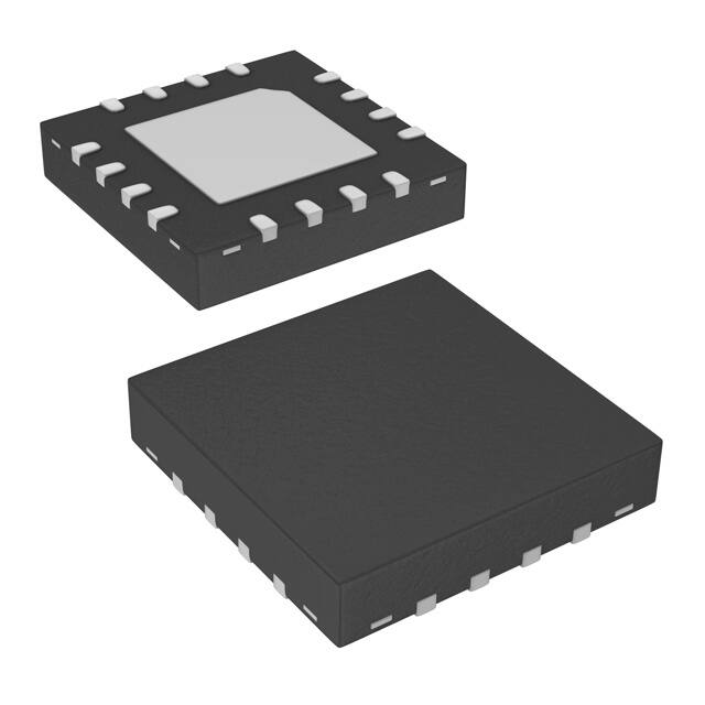


 工商网监
湘ICP备2023018690号
工商网监
湘ICP备2023018690号
