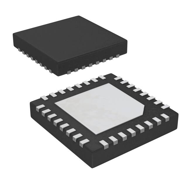
DATASHEET
ISL8126
FN7892
Rev.2.00
January 29, 2015
Dual/n-Phase Buck PWM Controller with Integrated Drivers
Features
The ISL8126 integrates two voltage-mode PWM leading-edge
modulation control with input feed-forward synchronous buck
PWM controllers to control dual independent voltage
regulators or a 2-phase single output regulator. It also
integrates current sharing control for the power module to
operate in parallel, which offers high system flexibility.
• Wide VIN range operation: 3V to 26.5V
- VCC operation from 3V to 5.60V
• Excellent output voltage regulation: 0.6V internal reference
• Frequency synchronization with programmable phase delay
up to 12-phase applications
The ISL8126 integrates an internal linear regulator, which
generates IC’s bias voltages for applications with only one
single supply rail. The internal oscillator is adjustable from
150kHz to 1.5MHz, and is able to synchronize to an external
clock signal for frequency synchronization and phase
paralleling applications. Its PLL circuit can output a
phase-shift-programmable clock signal for the system to be
expanded to 3-, 4-, 6- and 12- phases with desired interleaving
phase shift.
• Fault spreading capability for high system reliability
• Digital soft-start with precharged output start-up capability
• Dual independent channel enable inputs with precision
voltage monitor and voltage feed-forward capability
- Programmable input voltage POR and its hysteresis with a
resistor divider at EN input
• Extensive circuit protection functions: output overvoltage,
undervoltage, overcurrent protection, over-temperature and
pre-power-on-reset overvoltage protection option
The ISL8126’s Fault Spreading feature protects any channel
from overloading/stressing due to system faults or phase
failure. The undervoltage fault protection features are also
designed to prevent a negative transient on the output voltage
during falling down. This eliminates the Schottky diode that is
used in some systems for protecting the load device from
reversed output voltage damage.
Applications
• Power supply for Datacom/Telecom and POL
• Paralleling power module
• Wide and narrow input voltage range buck regulators
Related Literature
• TB389 “PCB Land Pattern Design and Surface Mount
Guidelines for QFN Packages”
0o
VIN
0o
180o
Vo
90o
ISL8126
VO2
ISL8126
ISL8126
VIN
VO
ISL8126
VO1
VIN
• AN1713, “ISL8126EVAL1Z Evaluation Board User Guide”
180o
DUAL REGULATOR
TWO-PHASE REGULATOR
270o
FOUR-PHASE REGULATOR
FIGURE 1. TYPICAL APPLICATION DIAGRAM
FN7892 Rev.2.00
January 29, 2015
Page 1 of 39
�ISL8126
Table of Contents
Pin Configuration. . . . . . . . . . . . . . . . . . . . . . . . . . . . . . . . . . . . . . . . . . . . . . . . . . . . . . . . . . . . . . . . . . . . . . . . . . . . . . . . . . . . . . . . . . . . 3
Functional Pin Descriptions. . . . . . . . . . . . . . . . . . . . . . . . . . . . . . . . . . . . . . . . . . . . . . . . . . . . . . . . . . . . . . . . . . . . . . . . . . . . . . . . . . . 3
Ordering Information . . . . . . . . . . . . . . . . . . . . . . . . . . . . . . . . . . . . . . . . . . . . . . . . . . . . . . . . . . . . . . . . . . . . . . . . . . . . . . . . . . . . . . . . 5
Controller Block Diagram . . . . . . . . . . . . . . . . . . . . . . . . . . . . . . . . . . . . . . . . . . . . . . . . . . . . . . . . . . . . . . . . . . . . . . . . . . . . . . . . . . . . . 6
Integrated Driver Block Diagram. . . . . . . . . . . . . . . . . . . . . . . . . . . . . . . . . . . . . . . . . . . . . . . . . . . . . . . . . . . . . . . . . . . . . . . . . . . . . . . 7
Typical Application Circuits . . . . . . . . . . . . . . . . . . . . . . . . . . . . . . . . . . . . . . . . . . . . . . . . . . . . . . . . . . . . . . . . . . . . . . . . . . . . . . . . . . . 8
2-Phase Operation with DCR Sensing . . . . . . . . . . . . . . . . . . . . . . . . . . . . . . . . . . . . . . . . . . . . . . . . . . . . . . . . . . . . . . . . . . . . . . . . . . . . . . . . .8
2-Phase Operation with rDS(ON) Sensing. . . . . . . . . . . . . . . . . . . . . . . . . . . . . . . . . . . . . . . . . . . . . . . . . . . . . . . . . . . . . . . . . . . . . . . . . . . . . .9
Dual Regulators with DCR Sensing and Remote Sense . . . . . . . . . . . . . . . . . . . . . . . . . . . . . . . . . . . . . . . . . . . . . . . . . . . . . . . . . . . . . . . . 10
Double Data Rate I or II . . . . . . . . . . . . . . . . . . . . . . . . . . . . . . . . . . . . . . . . . . . . . . . . . . . . . . . . . . . . . . . . . . . . . . . . . . . . . . . . . . . . . . . . . . 11
3-Phase Regulator with Precision Resistor Sensing . . . . . . . . . . . . . . . . . . . . . . . . . . . . . . . . . . . . . . . . . . . . . . . . . . . . . . . . . . . . . . . . . . . 12
4-Phase Operation with DCR Sensing . . . . . . . . . . . . . . . . . . . . . . . . . . . . . . . . . . . . . . . . . . . . . . . . . . . . . . . . . . . . . . . . . . . . . . . . . . . . . . . 13
Multiple Power Modules in Parallel with Current Sharing Control. . . . . . . . . . . . . . . . . . . . . . . . . . . . . . . . . . . . . . . . . . . . . . . . . . . . . . . . 14
3-Phase Regulator with Resistor Sensing and 1-Phase Regulator . . . . . . . . . . . . . . . . . . . . . . . . . . . . . . . . . . . . . . . . . . . . . . . . . . . . . . . 15
6-Phase Operation with DCR Sensing . . . . . . . . . . . . . . . . . . . . . . . . . . . . . . . . . . . . . . . . . . . . . . . . . . . . . . . . . . . . . . . . . . . . . . . . . . . . . . . 16
Absolute Maximum Ratings . . . . . . . . . . . . . . . . . . . . . . . . . . . . . . . . . . . . . . . . . . . . . . . . . . . . . . . . . . . . . . . . . . . . . . . . . . . . . . . . . . 17
Thermal Information . . . . . . . . . . . . . . . . . . . . . . . . . . . . . . . . . . . . . . . . . . . . . . . . . . . . . . . . . . . . . . . . . . . . . . . . . . . . . . . . . . . . . . . . 17
Recommended Operating Conditions . . . . . . . . . . . . . . . . . . . . . . . . . . . . . . . . . . . . . . . . . . . . . . . . . . . . . . . . . . . . . . . . . . . . . . . . . 17
Electrical Specifications . . . . . . . . . . . . . . . . . . . . . . . . . . . . . . . . . . . . . . . . . . . . . . . . . . . . . . . . . . . . . . . . . . . . . . . . . . . . . . . . . . . . 17
Typical Performance Curves . . . . . . . . . . . . . . . . . . . . . . . . . . . . . . . . . . . . . . . . . . . . . . . . . . . . . . . . . . . . . . . . . . . . . . . . . . . . . . . . . 21
Modes of Operation. . . . . . . . . . . . . . . . . . . . . . . . . . . . . . . . . . . . . . . . . . . . . . . . . . . . . . . . . . . . . . . . . . . . . . . . . . . . . . . . . . . . . . . . . 22
Functional Description . . . . . . . . . . . . . . . . . . . . . . . . . . . . . . . . . . . . . . . . . . . . . . . . . . . . . . . . . . . . . . . . . . . . . . . . . . . . . . . . . . . . . .
Initialization . . . . . . . . . . . . . . . . . . . . . . . . . . . . . . . . . . . . . . . . . . . . . . . . . . . . . . . . . . . . . . . . . . . . . . . . . . . . . . . . . . . . . . . . . . . . . . . . . . . .
Voltage Feed-forward . . . . . . . . . . . . . . . . . . . . . . . . . . . . . . . . . . . . . . . . . . . . . . . . . . . . . . . . . . . . . . . . . . . . . . . . . . . . . . . . . . . . . . . . . . . .
Soft-start . . . . . . . . . . . . . . . . . . . . . . . . . . . . . . . . . . . . . . . . . . . . . . . . . . . . . . . . . . . . . . . . . . . . . . . . . . . . . . . . . . . . . . . . . . . . . . . . . . . . . . .
PRE-POR Overvoltage Protection (PRE-POR-OVP) . . . . . . . . . . . . . . . . . . . . . . . . . . . . . . . . . . . . . . . . . . . . . . . . . . . . . . . . . . . . . . . . . . . . .
Over-Temperature Protection (OTP) . . . . . . . . . . . . . . . . . . . . . . . . . . . . . . . . . . . . . . . . . . . . . . . . . . . . . . . . . . . . . . . . . . . . . . . . . . . . . . . .
Overcurrent Protection . . . . . . . . . . . . . . . . . . . . . . . . . . . . . . . . . . . . . . . . . . . . . . . . . . . . . . . . . . . . . . . . . . . . . . . . . . . . . . . . . . . . . . . . . . .
Current Sharing Loop . . . . . . . . . . . . . . . . . . . . . . . . . . . . . . . . . . . . . . . . . . . . . . . . . . . . . . . . . . . . . . . . . . . . . . . . . . . . . . . . . . . . . . . . . . . .
Current Share Control in Multiphase Single Output with Shared COMP Voltage. . . . . . . . . . . . . . . . . . . . . . . . . . . . . . . . . . . . . . . . . . . .
Current Share Control Loop in Multi-Module with Independent Voltage Loop . . . . . . . . . . . . . . . . . . . . . . . . . . . . . . . . . . . . . . . . . . . . . .
Internal Series Linear and Power Dissipation . . . . . . . . . . . . . . . . . . . . . . . . . . . . . . . . . . . . . . . . . . . . . . . . . . . . . . . . . . . . . . . . . . . . . . . .
Oscillator . . . . . . . . . . . . . . . . . . . . . . . . . . . . . . . . . . . . . . . . . . . . . . . . . . . . . . . . . . . . . . . . . . . . . . . . . . . . . . . . . . . . . . . . . . . . . . . . . . . . . . .
Frequency Synchronization and Phase Lock Loop . . . . . . . . . . . . . . . . . . . . . . . . . . . . . . . . . . . . . . . . . . . . . . . . . . . . . . . . . . . . . . . . . . . .
Differential Amplifier for Remote Sensing . . . . . . . . . . . . . . . . . . . . . . . . . . . . . . . . . . . . . . . . . . . . . . . . . . . . . . . . . . . . . . . . . . . . . . . . . . .
Internal Reference and System Accuracy. . . . . . . . . . . . . . . . . . . . . . . . . . . . . . . . . . . . . . . . . . . . . . . . . . . . . . . . . . . . . . . . . . . . . . . . . . . .
DDR and Dual Mode Operation . . . . . . . . . . . . . . . . . . . . . . . . . . . . . . . . . . . . . . . . . . . . . . . . . . . . . . . . . . . . . . . . . . . . . . . . . . . . . . . . . . . .
25
25
25
26
28
28
29
30
31
32
32
33
33
34
35
36
Layout Considerations . . . . . . . . . . . . . . . . . . . . . . . . . . . . . . . . . . . . . . . . . . . . . . . . . . . . . . . . . . . . . . . . . . . . . . . . . . . . . . . . . . . . . .
Routing UGATE, LGATE and PHASE Traces. . . . . . . . . . . . . . . . . . . . . . . . . . . . . . . . . . . . . . . . . . . . . . . . . . . . . . . . . . . . . . . . . . . . . . . . . . .
Current Sense Component Placement and Trace Routing. . . . . . . . . . . . . . . . . . . . . . . . . . . . . . . . . . . . . . . . . . . . . . . . . . . . . . . . . . . . . .
General PowerPAD Design Considerations . . . . . . . . . . . . . . . . . . . . . . . . . . . . . . . . . . . . . . . . . . . . . . . . . . . . . . . . . . . . . . . . . . . . . . . . . .
36
37
37
37
Revision History. . . . . . . . . . . . . . . . . . . . . . . . . . . . . . . . . . . . . . . . . . . . . . . . . . . . . . . . . . . . . . . . . . . . . . . . . . . . . . . . . . . . . . . . . . . . 38
About Intersil . . . . . . . . . . . . . . . . . . . . . . . . . . . . . . . . . . . . . . . . . . . . . . . . . . . . . . . . . . . . . . . . . . . . . . . . . . . . . . . . . . . . . . . . . . . . . . 38
Package Outline Drawing . . . . . . . . . . . . . . . . . . . . . . . . . . . . . . . . . . . . . . . . . . . . . . . . . . . . . . . . . . . . . . . . . . . . . . . . . . . . . . . . . . . . 39
FN7892 Rev.2.00
January 29, 2015
Page 2 of 39
�ISL8126
Pin Configuration
FB1
VMON1
VSEN1-
VSEN1+
ISEN1B
ISEN1A
VCC
BOOT1
ISL8126
(32 LD QFN)
TOP VIEW
32
31
30
29
28
27
26
25
COMP1
1
24 UGATE1
ISET
2
23 PHASE1
ISHARE
3
22 LGATE1
EN/VFF1
4
21 PVCC
FSYNC
5
EN/VFF2
6
19 PHASE2
CLKOUT/REFIN
7
18 UGATE2
PGOOD
8
17 BOOT2
GND
9
10
11
12
13
14
15
16
COMP2
FB2
VMON2
VSEN2-
VSEN2+
ISEN2B
ISEN2A
VIN
20 LGATE2
Functional Pin Descriptions
PIN
NUMBER
SYMBOL
DESCRIPTION
1, 9
COMP1, COMP2
These pins are the error amplifier outputs. They should be connected to FB1, FB2 pins through desired
compensation networks when both channels are operating independently. When VSEN1-, VSEN2- are
pulled within 400mV of VCC, the corresponding error amplifier is disabled and its output (COMP pin) is high
impedance. Thus, in multiphase operations, all other SLAVE phases’ COMP pins can tie to the MASTER
phase’s COMP1 pin (1st phase), which modulates each phase’s PWM pulse with a single voltage feedback
loop. While the error amplifier is not disabled, an independent compensation network is required for each
cascaded IC.
2
ISET
This pin along with ISHARE pin are used for multiple ISL8126 current sharing purposes. When in 2-phase
mode (VSEN2- pulled within 400mV of VCC), this pin sources a current which is a combination of 15µA
constant offset current, current correction current (more details on “Current Share Control in Multiphase
Single Output with Shared COMP Voltage” on page 31), and the average of both sensed channel currents.
When in Dual-output mode, this pin sources a current, which is a combination of 15µA constant offset
current, current correction current and Channel 1’s sensed current. The current sourced out from this pin
and an external resistor (RISET) set the voltage at this pin (VISET). The RISET is recommended to be 10kΩ.
A noise decoupling capacitor less than 100pF can be added in parallel with the 10kΩ RISET.
In the single IC configuration (both 2-phase mode and dual-output mode), this pin can be tied to the ISHARE
pin.
3
ISHARE
This pin is used for current sharing purposes and is configured to the current share bus representing all
modules’ average current. When in 2-phase mode (VSEN2- pulled within 400mV of VCC), this pin sources
a current, which is a combination of 15µA constant offset current and the average of both sensed channel
currents. When in Dual-output mode, this pin sources a current, which is a combination of 15µA constant
offset current and Channel 1’s sensed current.
The share bus (ISHARE pins connected together) voltage (VISHARE) set by an external resistor (RISHARE)
represents the average current level of all ISL8126 controller connected to the current share bus. The share
bus impedance RISHARE should be set as RISET/NCTRL (RISET divided by number of ISL8126 in current
sharing controllers).
There is a 1.2V threshold for average overcurrent protection on this pin. VISHARE is compared with a 1.2V
threshold for average overcurrent protections.
When the fault condition on Channel 1 is detected or EN/VFF1 is pulled below its POR, ISHARE is internally
pulled to VCC.
FN7892 Rev.2.00
January 29, 2015
Page 3 of 39
�ISL8126
Functional Pin Descriptions (Continued)
PIN
NUMBER
SYMBOL
DESCRIPTION
4, 6
EN/VFF1, EN/VFF2
These pins have triple functions. The voltage on EN/VFF_ pin is compared with a precision 0.8V threshold
for system enable to initiate soft-start. With a voltage lower than the threshold, the corresponding channel
can be disabled independently. By connecting these pins to the input rail through a voltage resistor divider,
the input voltage can be monitored for UVLO (undervoltage lockout) function. The undervoltage lockout and
its hysteresis levels can be programmed by these resistor dividers. The voltages on these pins are also fed
into the controller to adjust the sawtooth amplitude of each channel independently to realize the
feed-forward function.
Furthermore, during fault (such as overvoltage, overcurrent, and over-temperature) conditions, these pins
(EN/VFF_) are pulled low to communicate the information to other cascaded ICs.
5
FSYNC
The oscillator switching frequency is adjusted by placing a resistor (RFS) from this pin to GND. The internal
oscillator will lock to an external frequency source if this pin is connected to a switching square pulse
waveform, typically the CLKOUT signal from another ISL8126 or an external clock. The internal oscillator
synchronizes with the leading edge of the input signal.
7
CLKOUT/REFIN
This pin has a dual function depending on the mode in which the chip is operating. It provides a clock signal
to synchronize with other ISL8126(s) with its VSEN2- pulled within 400mV of VCC for multiphase (3-, 4-, 6-,
8-, 10-, or 12-phase) operation. When the VSEN2- pin is not within 400mV of VCC, ISL8126 is in dual mode
(dual independent PWM output). The clockout signal of this pin is not available in this mode, but the
ISL8126 can be synchronized to external clock. In dual mode, this pin works as the following two functions:
1. An external reference (0.6V target only) can be in place of the Channel 2’s internal reference through
this pin for DDR/tracking applications.
2. The ISL8126 operates as a dual-PWM controller for two independent regulators with selectable phase
degree shift, which is programmed by the voltage level on REFIN (see “DDR and Dual Mode Operation”
on page 36).
8
PGOOD
32, 10
FB1, FB2
These pins are the inverting inputs of the error amplifiers. These pins should be connected to VMON1,
VMON2 with the compensation feedback network. No direct connection between FB and VMON pins is
allowed. With VSEN2- pulled within 400mV of VCC, the corresponding error amplifier is disabled and the
amplifier’s output is high impedance. FB2 is one of the two pins to determine the relative phase
relationship between the internal clock of both channels and the CLKOUT signal. See Table 1 on page 23.
31, 11
VMON1, VMON2
These pins are outputs of the differential amplifiers. They are connected internally to the OV/UV/PGOOD
comparators. These pins should be connected to the FB1, FB2 pins by a standard feedback network when
both channels are operating independently. When VSEN1-, VSEN2- are pulled within 400mV of VCC, the
corresponding differential amplifier is disabled and its output (VMON pin) is high impedance. In such an
event, the VMON pins can be used as additional monitors of the output voltage with a resistor divider to
protect the system against single point of failure, which occurs in the system using the same resistor
divider for both of the UV/OV comparator and output voltage feedback.
30, 12
VSEN1-, VSEN2-
These pins are the negative inputs of standard unity gain operational amplifier for differential remote
sense for the corresponding regulator (Channels 1 and 2), and should be connected to the negative rail of
the load.
When VSEN1-, VSEN2- are pulled within 400mV of VCC, the corresponding error amplifier and differential
amplifier are disabled and their outputs are high impedance. Both VSEN2+ and FB2 input signal levels
determine the relative phases between the internal controllers as well as the CLKOUT signal (see Table 1
on page 23).
When configured as multiple power modules (each module with independent voltage loop) operating in
parallel, in order to implement the current sharing control, a resistor needs to be inserted between the
VSEN1- pin and the output voltage negative sense point (between VSEN1- and lower voltage sense resistor),
as shown in the “Typical Application Circuits” “Multiple Power Modules in Parallel with Current Sharing
Control” on page 14. This introduces a correction voltage for the modules with lower load current to keep
the current distribution balanced among modules. The module with the highest load current will
automatically become the master module. The recommended value for the VSEN1- resistor is 100Ω and it
should not be large in order to keep the unit gain amplifier input impedance compatibility. A capacitor is
also recommended to place in parallel with the 100Ω.
FN7892 Rev.2.00
January 29, 2015
Provides an open drain Power-Good signal when both channels are within 9% of the nominal output
regulation point with 4% hysteresis (13%/9%) and soft-start complete. PGOOD monitors the outputs
(VMON1/2) of the internal differential amplifiers.
Page 4 of 39
�ISL8126
Functional Pin Descriptions (Continued)
PIN
NUMBER
SYMBOL
DESCRIPTION
29, 13
VSEN1+, VSEN2+
These pins are the positive inputs of the standard unity gain operational amplifier for differential remote
sense for the corresponding channel (Channels 1 and 2), and should be connected to the positive rail of the
load. These pins can also provide precision output voltage trimming capability by pulling a resistor from
this pin to the positive rail of the load (trimming down) or the return (typical VSEN1-, VSEN2- pins) of the
load (trimming up). By setting the resistor divider connected from the output voltage to the input of the
differential amplifier, the desired output voltage can be programmed. To minimize the system accuracy
error introduced by the input impedance of the differential amplifier, a resistor below 1kΩ is recommended
to be used for the lower leg (ROS) of the feedback resistor divider.
The typical input impedance of VSEN+ with respect to VSEN- is 500kΩ. With VSEN2- pulled within 400mV
of VCC, the corresponding error amplifier is disabled and VSEN2+ is one of the two pins to determine the
relative phase relationship between the internal clock of both channels and the CLKOUT signal. See Table 1
on page 23 for details.
28, 14
ISEN1B, ISEN2B
These pins are the inverting (-) inputs of the current sensing amplifiers to provide rDS(ON), DCR, or precision
resistor current sensing together with the ISEN1A, ISEN2A pins. Refer to “2-Phase Operation with rDS(ON)
Sensing” on page 9 for rDS(ON) sensing set up and “2-Phase Operation with DCR Sensing” on page 8 for
DCR sensing set up.
27, 15
ISEN1A, ISEN2A
These pins are the non-inverting (+) inputs of the current sensing amplifiers to provide rDS(ON), DCR, or
precision resistor current sensing together with the ISEN1B, ISEN2B pins.
16
VIN
This pin is the input of the internal linear regulator. It should be tied directly to the input rail. The internal
linear device is protected against reverse bias generated by the remaining charge of the decoupling
capacitor at PVCC when losing the input rail. When used with an external 3.3V to 5V supply, this pin can be
tied directly to PVCC to bypass the internal LDO.
25, 17
BOOT1, BOOT2
These pins provide the bootstrap biases for the high-side drivers. Internal bootstrap diodes connected to
the PVCC pin provide the necessary bootstrap charge. Its typical operational voltage range is 2.5V to 5.6V.
24, 18
UGATE1, UGATE2
These pins provide the gate signals to drive the high-side devices and should be connected to the MOSFETs’
gates.
23, 19
PHASE1, PHASE2
Connect these pins to the source of the high-side MOSFETs and the drain of the low-side MOSFETs. These
pins represent the return path for the high-side gate drives.
22, 20
LGATE1, LGATE2
These pins provide the drive for the low-side devices and should be connected to the MOSFETs’ gates.
21
PVCC
This pin is the output of the internal series linear regulator. It provides the bias for both low-side and
high-side drives. Its operational voltage range is 3V to 5.6V. A 10µF ceramic capacitor is required for
decoupling PVCC to ground.
26
VCC
This pin provides bias power for the analog circuitry. An RC filter is recommended between the connection
of this pin to a 3V to 5.6V bias (typically PVCC). R is suggested to be a 5Ω resistor. And in 3.3V applications,
the R could be shorted to allow the low end input in concerns of the VCC falling threshold. The VCC
decoupling capacitor is strongly recommended to be a low ESR ceramic capacitor. This pin can be powered
either by the internal linear regulator or by an external voltage source.
EPAD
GND
The bottom pad is the signal and power ground plane. All voltage levels are referenced to this pad. This pad
provides a return path for the low-side MOSFET drives and internal power circuitries as well as all analog
signals. Connect this pad to the circuit ground with the shortest possible path (more than 5 to 6 vias to the
internal ground plane, placed on the soldering pad are recommended).
Ordering Information
PART NUMBER
(Notes 1, 2, 3)
ISL8126CRZ
PART MARKING
TEMP RANGE
(°C)
PACKAGE
(RoHS Compliant)
PKG.
DWG. #
ISL8126 CRZ
0 to +70
32 Ld 5x5 QFN
L32.5x5B
ISL8126IRZ
ISL8126 IRZ
-40 to +85
32 Ld 5x5 QFN
L32.5x5B
ISL8126EVAL1Z
Evaluation Board
NOTES:
1. Add “-T*” suffix for tape and reel. Please refer to TB347 for details on reel specifications.
2. These Intersil Pb-free plastic packaged products employ special Pb-free material sets, molding compounds/die attach materials, and 100% matte
tin plate plus anneal (e3 termination finish, which is RoHS compliant and compatible with both SnPb and Pb-free soldering operations). Intersil
Pb-free products are MSL classified at Pb-free peak reflow temperatures that meet or exceed the Pb-free requirements of IPC/JEDEC J STD-020.
3. For Moisture Sensitivity Level (MSL), please see device information page for ISL8126. For more information on MSL please see techbrief TB363.
FN7892 Rev.2.00
January 29, 2015
Page 5 of 39
�ISL8126
Controller Block Diagram
PGOOD
VCC
VIN
8
26
16
EN1
EN2
VMON1
VMON2
CH1_FAULT
CH2_FAULT
PGOOD
CIRCUIT
VCC
-
INTERNAL
LINEAR REGULATOR
POWER-ON
RESET
21 PVCC
SAW1
400mV
25 BOOT1
ICSH_CORR
VSEN1- 30
INT. VREF
-
-
-
MOSFET
DRIVER
E/A
SS1
VSEN1+ 29
23 PHASE1
PWM1
CURRENT
BALANCE
CIRCUIT
VMON1 31
FB1 32
PWM1 1
CHANNEL
CURRENT
SAMPLING
COMP1 1
INT. VREF
EN_TH
-
-
CHANNEL 1
CH1
OCP
SOFT-START AND
FAULT LOGIC
EN1
EN/VFF1 4
22 LGATE1
Ch1 Fault
IAVG_CS ICS1 ICSH_ERR
OV/UV
COMP1
24 UGATE1
27 ISEN1A
28 ISEN1B
ICS1
-
7-CYCLE
DELAY
111µA
AVG_OCP
IEN_HYS
1.2V
-
EN/VFF1 EN/VFF2
SAW1
MASTER CLOCK
OSCILLATOR
GENERATOR
FSYNC 5
VCC
400mV
RELATIVE
PHASE
CONTROL
M/D CONTROL
VSEN2- 12
CURRENT
SHARE
BLOCK
ICSH_ERR
ISHARE
2
ISET
ICS1
AVERAGE
ICS2
CURRENT
IAVG_CS+15µA
M/D = 1 (Multiphase operation) : IAVG_CS = (ICS1+ICS2) / 2
M/D = 0 (Dual-output Operation): IAVG_CS = ICS1
PVCC
-
SAW2
VSEN2+ FB2
VSEN2+ 13
17 BOOT2
VMON2 11
E/A
CURRENT
BALANCE
CIRCUIT
COMP2 9
INT. VREF
-
EN/VFF2 6
EN2
OV/UV
COMP2
MOSFET
DRIVER
PWM2
SS2
FB2 10
EN_TH
3
M/D CONTROL
INT. VREF
CLKOUT/
7
REFIN
ICSH_CORR
CHANNEL 2
SOFT-START AND
FAULT LOGIC
IEN_HYS
AVG_OCP
CH2
OCP
IAVG_CS
ICS2
ICSH_ERR
7-CYCLE
DELAY
18 UGATE2
19 PHASE2
Ch2 Fault
20 LGATE2
111µA
ICS2
PWM1 2
CHANNEL
CURRENT
SAMPLING
15 ISEN2A
14 ISEN2B
M/D CONTROL
EP
FN7892 Rev.2.00
January 29, 2015
Page 6 of 39
�ISL8126
Integrated Driver Block Diagram
Channels 1 and 2 Gate Drive
PVCC
3Ω
BOOTn
UGATEn
PWMn
10kΩ
FAULT LOGIC
GATE
CONTROL
LOGIC
SHOOTTHROUGH
PROTECTION
PHASEn
10kΩ
LGATEn
FN7892 Rev.2.00
January 29, 2015
Page 7 of 39
�ISL8126
Typical Application Circuits
2-Phase Operation with DCR Sensing
VIN
+3V TO +26.5V
CHFIN
RCC
CF1
VCC
CBIN
CF2
PVCC
BOOT1
CBOOT1
UGATE1
VIN
Q1
LOUT1
VOUT0.8V, there will be current sourcing
out from the ISHARE pin, which represents the Channel 1 current
plus 15µA offset current.
MODE 3: When VSEN2- is used as a negative sense line, both
channels’ phase shift depends upon the voltage level of
CLKOUT/REFIN. When the CLKOUT/REFIN pin is within 29% to
45% of VCC, Channel 2 delays 0° over Channel 1 (Mode 3A);
when within 45% to 62% of VCC, there is a 90°delay (Mode 3B);
when greater than 62% to VCC, there is a 180° delay (Mode 3C).
Refer to the “DDR and Dual Mode Operation” on page 36.
MODE 4: When VSEN2- is used as a negative remote sense line,
and CLKOUT/REFIN is connected to an external voltage ramp
lower than the internal soft-start ramp and lower than 0.6V, the
external ramp signal will replace Channel 2’s internal soft-start
ramp to be tracked at start-up, controller operating in DDR mode.
The controller will use the lowest voltage among the internal 0.6V
reference, the external voltage in CLKOUT/REFIN pin and the
soft-start ramp signal. Channel 1 is delayed 60° behind
Channel 2. Refer to the “DDR and Dual Mode Operation” on
page 36.
MODE 5: With VSEN2- pulled within 400mV of VCC, FB2 pulled to
ground and VSEN2+ pulled either to VCC or GND, the internal
channels are 180° out-of-phase and operate in 2-phase single
output (Mode 5A). The CLKOUT/REFIN pin also signals out clock
with 60° phase shift (rising edge) relative to the Channel 1’s
clock signal (falling edge of PWM) for 6-phase operation with two
other ISL8126s (Mode 5B). When the share pins are not
connected to each other for the three ICs in sync, two of which
FN7892 Rev.2.00
January 29, 2015
25
-50
-25
0
25
50
75
100
125
150
TEMPERATURE (°C)
FIGURE 9. EN/VFF2 HYSTERESIS CURRENT vs TEMPERATURE
can operate in Mode 5A. The 3rd IC can be operated in Mode 3 to
generate 3 independent outputs (Mode 5C), or the 3rd IC can
also be operated in Mode 4 to generate 4 independent outputs
(Mode 5D).
MODE 6: With VSEN2- pulled within 400mV of VCC, FB2 pulled to
VCC and VSEN2+ pulled to GND, the internal channels (as 1st and
3rd Phase, respectively) are 240° out-of-phase. The
CLKOUT/REFIN pin signals out 120° relative phases to the falling
edge of Channel 1’s clock signal to synchronize with the second
ISL8126’s Channel 1 (as 2nd Phase). This allows 3-phase single
output configuration to be constructed using two ISL8126s.
MODE 7: With VSEN2- pulled within 400mV of VCC and both of
FB2 and VSEN2+ pulled to VCC, the internal channel is 180°
out-of-phase. The CLKOUT/REFIN pin signals out (rising edge)
90° relative phase to the Channel 1’s clock signal (falling edge of
PWM) to synchronize with another ISL8126, which can operate
at Mode 3, 4, 5A, or 7A. A 4-phase single output converter can be
constructed with two ISL8126s operating in Mode 5A or 7A
(Mode 7A). If the share bus is not connected between ICs, each IC
could generate an independent output (Mode 7B). When the
second ISL8126 operates as two independent regulators
(Mode 3) or in DDR mode (Mode 4), then a three independent
output system is generated (Mode 7C). Both ICs can also be
constructed as a 3-phase converter (0°, 90°, and 180°, not an
equal phase shift for 3-phase) with a single phase regulator
(270°).
MODE 8: The output CLKOUT signal allows expansion for
12-phase operation with the cascaded sequencing, as shown in
Table 1. No external clock is required in this mode for the desired
phase shift.
MODE 9: With an external clock, the part can be expanded for 5,
7, 8, 9 10 and 11 phase single output operation with the desired
phase shift.
Page 22 of 39
�1ST IC (I = INPUT; O = OUTPUT; I/O = INPUT AND OUTPUT, BIDIRECTION)
MODE
EN/
VFF1
EN/
VFF2
VSEN2- (I)
FB2 (I)
VSEN2+ (I)
CLKOUT/REFIN WRT
1ST (I or O)
MODES OF OPERATION
ISHARE (I/O) REPRESENTS
OUTPUT (See
WHICH CHANNEL(S)
2ND CHANNEL WRT 1ST OPERATION MODE OPERATION MODE
of 3RD IC
of 2ND IC
Description for Details)
CURRENT
(O) (Note 10)
1
0.8V
0.8V
>0.8V
0.8V
>0.8V
62% of VCC (I)
1ST CHANNEL
180°
-
-
DUAL REGULATOR
4
>0.8V
>0.8V
12)
NOTES:
10. “2ND CHANNEL WRT 1ST” is referred to as “channel 2 lag channel 1 by the degrees specified by the number in the corresponding table cells”. For example, 90° with 2ND CHANNEL WRT 1ST
means channel 2 lags channel 1 by 90°; -60° with 2ND CHANNEL WRT 1ST means channel 2 leads channel 1 by 60°.
11. All EN/VFF pins are tied together.
ISL8126
FN7892 Rev.2.00
January 29, 2015
TABLE 1.
Page 23 of 39
�ISL8126
CH1 UG (1ST IC)
D
1-D
180°
CH2 UG (1ST IC)
D
90°
50%
CLKOUT (1ST IC)
90°
D
CH1 UG (2ND IC)
180°
CH2 UG (2ND IC)
D
4 PHASE TIMING DIAGRAM (MODE 7A)
CH1 UG (1ST IC)
D
1-D
240°
D
CH2 UG (1ST IC)
120°
CLKOUT (1ST IC)
50%
120°
CH1 UG (2ND IC)
1-D
D
CH2 UG (2ND IC, OFF, EN/VFF2 = 0)
3-PHASE TIMING DIAGRAM (MODE 6)
VCC
VSEN2- VSEN2+
FB2
VMON2
CLKOUT/REFIN
COMP2
400mV
DIFF
AMP2
UV/OV
COMP2
ERROR
AMP2
VREF2 = VREF
CLOCK GENERATOR
AND
RELATIVE PHASES CONTROL
CHANNEL 1
PWM CONTROL
BLOCK
CHANNEL 2
PWM CONTROL
BLOCK
FIGURE 10. SIMPLIFIED RELATIVE PHASES CONTROL
FN7892 Rev.2.00
January 29, 2015
Page 24 of 39
�ISL8126
Functional Description
Initialization
Initially, the ISL8126 Power-On Reset (POR) circuits continually
monitor the bias voltages (PVCC and VCC) and the voltage at the
EN/VFF pin. The POR function initiates soft-start operation 192
clock cycles after the following conditions are met:
• VCC and PVCC voltages exceed their POR thresholds.
• PLL locking time has expired.
• EN/VFF pin voltage is pulled to be above 0.8V.
• For Channel 1 only, ISHARE voltage must fall below 70%
(typical) of VCC.
ISHARE is also pulled to VCC when Channel1 detects fault
conditions or EN/VFF1 is below its POR threshold. ISHARE is
released from VCC after EN/VFF1’s voltage higher than its POR
threshold for 16 switching cycles; therefore, there is 176 cycles
delay from ISHARE falls to 0.7*VCC to the beginning of soft-start.
During shutdown or fault conditions, the soft-start is reset quickly
while UGATE and LGATE change states immediately (120%
OR
AND
MULTIPHASE
MODE = HIGH
87%
PGOOD1
FORCE
LGATE1
HIGH
AND
EN/VFF1
VMON2
113%
AND
OR
EN/VFF2
FORCE
LGATE2
HIGH
VMON2 > 120%
CH1 SOFT-START DONE
VMON2
VMON1
FIGURE 18. FORCE LGATE HIGH LOGIC
PGOOD2
120%
CH2 SOFT-START DONE
VOUT
EN1
3 CYCLES
PGOOD1
3 CYCLES
PGOOD
PGOOD
EN2
UV
OV LATCH
PGOOD2
PGOOD1
PGOOD2
UGATE AND EN/VFF LATCH LOW
FIGURE 19. PGOOD TIMING UNDER UV AND OV
+20%
VMON1, 2
+13%
+9%
VREF
-9%
-13%
PGOOD1, 2
PGOOD LATCH OFF
AFTER 120% OV
FIGURE 17. POWER-GOOD THRESHOLD WINDOW
The Overvoltage (OV) and Undervoltage (UV) protection circuitry
monitor the voltage on the VMON pins.
OV protection is active upon VCC POR. An OV condition (>120%)
would latch IC off (the high-side MOSFET to latch off
permanently; the low-side MOSFET turns on immediately at the
time of OV trip and then turns off after the VMON drops below
87%). The EN/VFF and PGOOD are also latched low at OV event.
The latch condition can be reset only by recycling VCC. In
Dual/DDR mode, each channel is responsible for its own OV
event with the corresponding VMON as the monitor. In
multiphase mode, both channels respond simultaneously when
either triggers an OV event.
There is another non-latch OV protection (113% of target level).
At the condition of EN/VFF low and the output over 113% OV, the
lower side MOSFET will turn on until the output drops below 87%.
This is to protect the overall power trains in case of only one
channel of a multiphase system detecting OV. The low-side
MOSFET always turns on at the conditions of EN/VFF = LOW and
the output voltage above 113% (all VMON pins and EN/VFF pins
are tied together) and turns off after the output drops below 87%.
Thus, in a high phase count application (Multiphase Mode), all
cascaded ICs can latch off simultaneously via the EN/VFF pins
(EN/VFF pins are tied together in multiphase mode), and each IC
shares the same sink current to reduce the stress and eliminate
the bouncing among phases.
The UV functionality is not enabled until the end of soft-start. In a
UV event, if the output drops below -13% of the target level due to
FN7892 Rev.2.00
January 29, 2015
Page 27 of 39
�ISL8126
INDUCTOR DCR SENSING
VIN
UGATE(n)
+
(EQ. 2)
The resistor value should be as large as possible to minimize
power dissipation, while providing sufficient margin for the
internal 10kΩ and MOSFET’s Vth tolerances. For example, a 2kΩ
resistor is recommended for applications using logic-level
MOSFET with the maximum prebiased voltage less than 5V.
Over-Temperature Protection (OTP)
When the junction temperature of the IC is greater than +150°C
(typically), both EN/VFF pins pull low to inform other cascaded
channels via their EN/VFF pins. All connected EN/VFFs stay low
and release after the IC’s junction temperature drops below
+125°C (typically), with a +25°C hysteresis (typical).
INDUCTOR CURRENT SENSING
The ISL8126 supports inductor DCR sensing, MOSFET’s rDS(ON)
sensing, or resistive sensing techniques. The circuits shown in
Figures 20, 21, and 22 represent one channel of the controller.
This circuitry is identical for both channels.
Note that the common mode input voltage range of the current
sense amplifiers is VCC - 1.8V. Therefore, the rDS(ON) sensing
must be used for applications with output voltage greater than
VCC - 1.8V. For example, when VCC = 5.4V, the inductor DCR and
the resistive sensing configurations can be used for output
voltage less than 3V. For higher output voltage, rDS(ON) sensing
configuration must be used.
ISL8216
INTERNAL CIRCUIT
VL
+
VC(s)
R
I
VOUT
COUT
-
The PRE-POR-OVP works against prebiased start-up when
precharged output voltage is higher than the threshold of the
low-side MOSFET, however, it can be disabled by placing a
resistor from LGATE to ground. The resistor value can be
estimated from Equation 2.
DCR
INDUCTOR
LGATE(n)
When both the VCC and PVCC are below PORs (not including EN
POR), the UGATE is low and LGATE is floating (high impedance).
EN/VFF has no control on LGATE when VCC and PVCC are below
their PORs. When VCC and PVCC are above their PORs, the LGATE
would not be floating but toggling with its PWM pulses. An
internal 10kΩ resistor, connected in between PHASE and LGATE
nodes, implements the PRE-POR-OVP circuit. The output of the
converter that is equal to phase node voltage via output
inductors is then effectively clamped to the low-side MOSFET’s
gate threshold voltage, which provides some protection to the
load if the upper MOSFET(s) is shorted during start-up, shutdown,
or normal operations. For complete protection, the low-side
MOSFET should have a gate threshold that is much smaller than
the maximum voltage rating of the load.
FN7892 Rev.2.00
January 29, 2015
L
PHASE(n)
PRE-POR Overvoltage Protection
(PRE-POR-OVP)
10k
R -----------------------------------------------------------V pre – biased max
-------------------------------------------------- – 1
V th min
I s
L
-
some reason (cases when EN/VFF is not pulled low) other than
OV, OC, OT, and PLL faults, the lower MOSFETs will be turned on
for ~345ns for each switching cycle to avoid high negative
voltage ringing until the UN condition is removed.
C
CS n
RISEN(n)
(PTC)
SAMPLE
&
HOLD
+
-
ISEN(n)A
ISEN(n)B
ISEN
FIGURE 20. DCR SENSING CONFIGURATION
An inductor’s winding is characteristic of a distributed resistance
as measured by the DCR (Direct Current Resistance) parameter.
Consider the inductor DCR as a separate lumped quantity, as
shown in Figure 20. The inductor current, IL; will also pass
through the DCR. Equation 3 shows the s-domain equivalent
voltage across the inductor VL.
V L = I L s L + DCR
(EQ. 3)
A simple R-C network across the inductor extracts the DCR
voltage, as shown in Figure 20. The voltage on the capacitor VC,
can be shown to be proportional to the inductor current IL, see
Equation 4.
L
s ------------+ 1 DCR I L
DCR
V C = -------------------------------------------------------------------- s RC + 1
(EQ. 4)
If the R-C network components are selected such that the RC
time constant (= R*C) matches the inductor time constant
(= L/DCR), the voltage across the capacitor VC is equal to the
voltage drop across the DCR, i.e. proportional to the inductor
current. The value of R should be as small as feasible for best
signal-to-noise ratio. Make sure the resistor package size is
appropriate for the power dissipated and include this loss in
efficiency calculations. In calculating the minimum value of R,
the average voltage across C (which is the average ILDCR
product) is small and can be neglected. Therefore, the minimum
value of R may be approximated using Equation 5.
2
2
D V IN – max – V OUT + 1 – D V OUT
R min = ------------------------------------------------------------------------------------------------------------k P R – pkg P
(EQ. 5)
Where PR-pkg is the maximum power dissipation specification
for the resistor package and P is the derating factor for the
same parameter (eg.: PR-pkg = 0.063W for 0402 package,
P = 80% at +85°C). k is the margin factor, also to limit
Page 28 of 39
�ISL8126
temperature raise in the resistor package, recommend using 0.4.
Once Rmin has been calculated, solve for the maximum value of
C using Equation 6:
L
C max = -------------------------------R min DCR
(EQ. 6)
and choose the next-lowest readily available value. Then
substitute the chosen value into the same equation and
recalculate the value of R. Choose the 1% resistor standard value
closest to this recalculated value of R. For example, when
VIN_MAX = 14.4V, VOUT = 2.5V, L = 1µH and DCR = 1.5mΩ, with
0402 package Equation 5 yields RMIN of 1476Ω and Equation 6
yields CMAX of 0.45µF. By choosing 0.39µF and recalculating the
resistor it yields 1.69kΩ
With the internal low-offset current amplifier, the capacitor
voltage VC is replicated across the sense resistor RISEN.
Therefore, the current out of ISEN(n)B pin, ISEN, is proportional to
the inductor current. After 175ns blanking period with respect to
the falling edge of the PWM pulse of each channel, the ISEN
current is filtered and sampled for 175ns. The sampling current
ICS then can be derived as shown by Equation 7:
PHASE(n)
IL
VOUT
COUT
LGATE(n)
ISL8216A
INTERNAL CIRCUIT
I
CS n
RISEN(n)
SAMPLE
AND
HOLD
+
-
ISEN(n)A
ISEN(n)B
ISEN
FIGURE 21. SENSE RESISTOR IN SERIES WITH INDUCTOR
FN7892 Rev.2.00
January 29, 2015
MOSFET rDS(ON) SENSING
I
VIN
CS n
ISEN
IL
SAMPLE
AND
HOLD
ISEN(n)B
RISEN
(PTC)
+
ISEN(n)A
I x r DS ON
L
+
EXTERNAL CIRCUIT
FIGURE 22. MOSFET rDS(ON) CURRENT-SENSING CIRCUIT
For accurate current sense, a dedicated current-sense resistor
RSENSE in series with the output inductor can serve as the
current sense element (see Figure 21). This technique is more
accurate, but reduces overall converter efficiency due to the
additional power loss on the current sense element RSENSE.
RSENSE
Similar to DCR current sensing approach, the resistive sensing
approach can be used with output voltage less than VCC - 1.8V.
ISL8126 INTERNAL CIRCUIT
RESISTIVE SENSING
L
(EQ. 8)
(EQ. 7)
Where IL is the inductor DC current, fSW is the switching
frequency, and tMIN_OFF is 350ns.
UGATE(n)
V OUT
1–D
IL + ---------------- ---------------- – t MIN_OFF RSENSE
L
2F SW
ICS = -----------------------------------------------------------------------------------------------------------------------------R ISEN
N-CHANNEL
MOSFETs
V OUT
1–D
I L + ---------------- -------------- – t MIN_OFF DCR
L
2f
SW
ICS = -------------------------------------------------------------------------------------------------------------R ISEN
VIN
Equation 8 shows the sampling current, ICS, when using sensing
resistor.
The controller can also sense the channel load current by
sampling the voltage across the synchronous MOSFET rDS(ON)
(see Figure 22). The amplifier is ground-reference by connecting
the ISEN(n)A pin to the source of the synchronous MOSFET.
ISEN(n)B pin is connected to the synchronous MOSFET’S drain
through the current sense resistor RISEN. The voltage across
RISEN is equivalent to the voltage drop across the rDS(ON) of the
lower MOSFET while it is conducting. The resulting current out of
the ISEN(n)B pin is proportional to the channel current IL.
Equation 9 shows the sampling current, ICS, when using MOSFET
rDS(ON) sensing.
V OUT
1–D
I L + ---------------- ---------------- – t MIN_OFF r DS ON
L
2F
SW
I CS = ------------------------------------------------------------------------------------------------------------------------R ISEN
(EQ. 9)
Both inductor DCR and MOSFET rDS(ON) value will increase as the
temperature increases. Therefore, the sensed current will
increase as the temperature of the current sense element
increases. In order to compensate the temperature effect on the
sensed current signal, a Positive Temperature Coefficient (PTC)
resistor can be selected for the sense resistor RISEN.
Overcurrent Protection
For overload and hard short condition, the overcurrent protection
reduces the regulator RMS output current much less than full
load by putting the controller into hiccup mode. A delay time,
equal to 3 soft-start intervals, is inserted to allow the disturbance
to be cleared out. After the delay time, the controller then
initiates a soft-start interval. If the output voltage comes up and
returns to the regulation, PGOOD transitions high. If the OC trip is
Page 29 of 39
�ISL8126
exceeded during the soft-start interval, the controller pulls
EN/VFF low again. The PGOOD signal will remain low and the
soft-start interval will be allowed to expire. Another soft-start
interval will be initiated after the delay interval. If an overcurrent
trip occurs again, this same cycle repeats until the fault is
removed.
The OCP function is enabled at start-up. The ISL8126 monitors 2
signals: sampled channel current, ICS, and ISHARE voltage for
overcurrent protection.
CHANNEL CURRENT OCP
Each sampled channel current, ICS, is compared to 111µA (typ.)
for the OCP trip point. The channel overcurrent trip point can be
set by using RISEN value such that the overcurrent trip point
corresponds to the channel sensing current, ICS, of 111µA. For
DCR current sensing, Equation 7, and rDS(ON) current sensing,
Equation 9, the RISEN can be estimated from Equations 10 and
11, respectively.
V OUT
1–D
IOC + ---------------- ---------------- – t MIN_OFF DCR
L
2F
SW
R ISEN = ----------------------------------------------------------------------------------------------------------------------111A
(EQ. 10)
In multiphase operation, the VISHARE represents the average
current of all ISL8126 and compares with the ISHARE pin precision
1.2V threshold to determine the overcurrent condition. At the same
time, each channel has an additional overcurrent trip point at
111µA with 7-cycle delay for channel overcurrent protection. This
scheme helps protect against loss of channel(s) in multiphase mode
so that no single channel could carry excessive current in such
event. With RISHARE = 10kΩIt would make the channel current
OCP and ISHARE OCP trip at the same over current level; (111µA +
15µA) x 10kΩ1.26V.
Note that it is not necessary for the RISHARE to be scaled to trip at
the same level as the 111µA OCP comparator if the application
allows. For instance, when Channel 1 operates independently, the
OC trip set by 1.2V comparator can be lower than 111µA trip point.
To set the ISHARE OCP in the multiphase configuration, the RISEN
must be determined first by using Equations 10 or 11. The IOC is
the overcurrent for each phase, which is approximately
IOC_total/number of phases. Upon determining RISET, Equations 7,
8, 9, and 11 can be used to determine ISHARE OCP, as shown in
Equation 13.
1.2V
R ISHARE = ----------------------------------------------------------------------N
CNTL
V OUT
1–D
IOC + ---------------- ---------------- – t MIN_OFF r DS ON
L
2FSW
R ISEN = -------------------------------------------------------------------------------------------------------------------------------111A
(EQ. 11)
While configured as multiphase operation (VSEN2- > VCC - 400mV),
the channel OCP has 7 clock cycles delay before entering hiccup
mode.
In dual-output operation, the 7-clock cycle delay on Channel 2 is
bypassed so the circuit responds to over current condition
immediately. In this mode, the 7-clock cycle delay in Channel1 is
still active. The fast OCP response on Channel1 will be rely on the
OCP on ISHARE pin where the voltage on this pin represents the
Channel1 current.
During soft-start period with VMON1 less than 0.4V, the OCP
threshold on the sampled channel current, ICS, of both channels
are increased to 222µA (typ.) to compensate the in-rush current.
ISHARE OCP
Refer to the “Controller Block Diagram” on page 6, ISHARE pin
sources out a current IAVG_CS with 15µA offset. In the 2-phase
mode, IAVG_CS is the average of both Channels 1 and 2 sampled
currents as calculated in Equation 12.
(EQ. 12)
While in the dual-output mode, IAVG_CS is a copy of Channel1’s
sampled current.
FN7892 Rev.2.00
January 29, 2015
i
(EQ. 13)
i=1
Without temperature compensation, the OCP trip point should be
evaluated based on the DCR or MOSFET rDS(ON) values at the
maximum device’s temperature.
ICS1 + ICS2
IAVG_CS = ----------------------------------2
I AVG_CS + 15A
R ISET = R ISHARE N CNTL
where NCNTL is the number of the ISL8126 controllers in parallel
or multiphase operations.
For the RISEN chosen for OCP setting, the final value is usually
higher than the number calculated from Equation 9. The PCB and
inductor pad soldering resistance would affect the total
impedance a lot especially at low DCR applications.
Current Sharing Loop
When the ISL8126 operates in 2-phase mode (VSEN2- is pulled
within VCC - 400mV), the current control loop keeps Channel 1
and Channel 2 currents in balance. The sensed currents from
both channels are combined to create an average current
reference (IAVG), which represents average current of both
channel currents. The signal IAVG is then subtracted from the
individual sensed current (ICS1 or ICS2) to produce a current
correction signal for each channel. The block diagram of current
sharing control circuit is shown in Figure 23.
When both channels operate independently, the average
function is disabled, and the current correction block of
Channel 2 is also disabled. The IAVG_CS is Channel 1 sensed
current ICS1. Channel 1 makes any necessary current correction
by comparing the voltages at ISET and ISHARE pins (for 3-phase,
two ISL8126s configuration).
When the share bus does not connect to other ICs, the ISET and
ISHARE pins can be shorted together and grounded via a single
resistor to ensure zero share error.
Page 30 of 39
�ISL8126
IAVG = (ICS1 + ICS2) / 2
IAVG_CS = IAVG or ICS1
ERROR AMP 1 +
ISHARE = IAVG_CS + 15µA
ISET = IAVG_CS + 15µA + ICSH_ERR
ICS1
IAVG_CS
-
+
CURRENT
CORRECTION
BLOCK
-
CURRENT
MIRROR
BLOCK
SHARE BUS
RISHARE
-
ICS2
ICSH_ERR -
ICSH_ERR
20mV
ISHARE
+
VERROR1
CURRENT
MIRROR
BLOCK
IAVG_CS+15µA
ISET
+
-
+
ICSH_ERR
+
-
IAVG_CS+15µA
RISET
ERROR AMP 2
+
ICSH_ERR
RISHARE=RISET/NCTRL
CURRENT
CORRECTION
BLOCK
-
IAVG_CS
VERROR2
VCC
400mV
+
VSEN2-
CURRENT
CORRECTION
BLOCK
+
VSEN1- VSEN1+
VMON1
FIGURE 23. SIMPLIFIED CURRENT SHARE AND INTERNAL BALANCE IMPLEMENTATION
Current Share Control in Multiphase Single
Output with Shared COMP Voltage
In multiphase/multi-IC implementation with one single error
amplifier for the voltage loop, all COMP pins must be tied
together. Therefore, all other channels’ error amplifiers that are
not used in voltage loop should be disabled with their
corresponding VSEN- pulled to VCC, as shown in Figure 24.
For current sharing purposes, all ISHARE pins must also be tied
together. The share bus (VISHARE) represents the average
current of all ISL8126s connected to the same ISHARE bus. The
ISHARE pin sources a copy of the IAVG_CS with 15µA offset
(IAVG_CS equals to IAVG or ICS1 depending upon the
configuration). The ISET pin sources out a copy of IAVG_CS,
ICSH_ERR and 15µA offset. ICSH_ERR on the ISET pin makes the
voltage at the ISET pin track the voltage at the ISHARE pin with
20mV offset. Thus, ICSH_ERR represents the difference of an
FN7892 Rev.2.00
January 29, 2015
individual ISL8126 current to the average current (ISHARE). The
current share error signal (ICSH_ERR) is then fed into the current
correction block to adjust each channel’s PWM pulse
accordingly.
If one single external resistor is used as RISHARE connecting the
ISHARE bus to ground for all the ICs in parallel, RISHARE should
be set equal to RISET/NCTRL (where NCNTL is the number of the
ISL8126 controllers in parallel or multiphase operations), and
the share bus voltage (VISHARE) set by the RISHARE, represents
the average current of all channels. RISHARE can also be set by
putting one resistor in each IC’s ISHARE pin and using the same
value with RISET (RISHARE = RISET), which results in the total
equivalent resistance value as RISET/NCTRL.
The current share function provides at least 10% overall accuracy
between ICs, 5% within the IC when using a 1% resistor to sense
a 10mV signal. The current share bus works for up to 12-phase.
Page 31 of 39
�ISL8126
VIN
REN/VFF_up
REN/VFF_low
With
voltage
loop
EN/VFF1,2 COM1/2
VSEN1+ CLKOUT
EN/VFF1,2 COM1/2
FSYNC
VSEN1/2-
VSEN1ISL81261
ISHARE ISET
VCC ISL81262
ISHARE
RISET1
RISHARE1
EN/VFF1,2 COM1/2
FSYNC
VSEN1/2-
ISET
VCC ISL81263
ISHARE ISET
CLKOUT
RISET3
RISET2
RISHARE2
RISHARE3
SHARE BUS
RISHARE_ = RISET_
FIGURE 24. SIMPLIFIED 6-PHASE SINGLE OUTPUT IMPLEMENTATION
Current Share Control Loop in Multi-Module
with Independent Voltage Loop
The power module controlled by ISL8126 with its own voltage
loop can be paralleled to supply one common output load with its
integrated Master-Slave current sharing control, as shown in the
“Typical Application Circuits” on page 14. A resistor RCSR and a
capacitor CCSR need to be inserted between VSEN1- pin and the
lower resistor of the voltage sense resistor divider for each
module. With this resistor, the correction current sourcing from
the VSEN1- pin will create a voltage offset to maintain even
current sharing among modules. The recommended value for the
VSEN1- resistor RCSR is 100Ω and it should not be large in order
to keep the unity gain amplifier input pin impedance
compatibility. The maximum source current from the VSEN1- pin
is 350µA, which is combined with RCSR to determine the current
sharing regulation range. The generated correction voltage on
RCSR is suggested to be within 5% of VREF (0.6V) to avoid fault
triggering of UV/OV and PGOOD during dynamic events. The
value for CCSR can be estimated from Equation 14.
35
C CSR = ----------------------------------R CSR F SW
(EQ. 14)
Where FSW is switching frequency.
It is recommended to have 3 analog signals: CLKOUT-SYNC,
ISHARE, and EN/VFF for communication among the paralleled
modules. All the modules are synchronized and the phase shift
can also be configured to optimal to reduce the input current
ripple by interleaving effects. The connections of these three
wires allows the system to be started at the same time and
achieve good current balance in start-up without overcurrent trip.
Internal Series Linear and Power Dissipation
The VIN pin is connected to PVCC with an internal series linear
regulator. The internal linear regulator’s input (VIN) can range
between 3V to 26.5V. PVCC pin is the output of the internal linear
regulator and it provides power for both the internal MOSFET
drivers. The PVCC and VIN pins should have the recommended
bypass ceramic capacitors (10µF) connected to GND for proper
operation. PVCC can be used to bias the IC analog circuitry, VCC,
FN7892 Rev.2.00
January 29, 2015
by connecting VCC to PVCC pin. The VCC pin should be connected
to the PVCC pin with an RC filter to prevent high frequency driver
switching noise into the analog circuitry. When the VIN drops
below 5.0V, the pass element will saturate; PVCC will track VIN
with a dropout of the linear regulator. When used with an
external supply less than 5V, the PVCC pin is recommended to be
tied directly to VIN.
2.65V TO 5.6V
2
3V TO 26.5V
10µF
1µF
PVCC
VCC
VIN
Z1
Z2
5V
FIGURE 25. INTERNAL REGULATOR IMPLEMENTATION
The LDO is capable of supplying 250mA with regulated 5.4V
output. In 3.3V input applications, when the VIN pin voltage is 3V,
the LDO can still supply 150mA while maintaining LDO output
voltage higher than VCC falling threshold to keep the IC
operating. Figure 4 shows the typical V-I curve of the internal
LDO. Note that the power dissipation in the device should not be
exceeded the package thermal limit. The power dissipation
inside the IC can be estimated with Equations 15 and 16.
Where the gate charge (QG1 and QG2) is defined at a particular
gate to source voltage (VGS1and VGS2) in the corresponding
MOSFET datasheet; IQ_VIN is the driver’s total quiescent current
with no load at drive outputs; NQ1 and NQ2 are number of upper
and lower MOSFETs, respectively.
Page 32 of 39
�ISL8126
P IC = VIN – PVCC I VIN + P DR
(EQ. 15)
0.27
0.24
Q G1 N Q1 Q G2 N Q2
I VIN = ------------------------------ + ------------------------------ PVCC F SW + I Q_VIN
V GS2
V GS1
(EQ. 16)
P DR = P DR_UP + P DR_LOW
R LO1
R HI1
P Qg_Q1
P DR_UP = -------------------------------------- + ---------------------------------------- --------------------2
R HI1 + R EXT1 R LO1 + R EXT1
R LO2
R HI2
P Qg_Q2
P DR_LOW = -------------------------------------- + ---------------------------------------- --------------------2
R HI2 + R EXT2 R LO2 + R EXT2
G
CDS
RGI1
CGS
Q1
S
PHASE
FIGURE 26. TYPICAL UPPER-GATE DRIVE TURN-ON PATH
PVCC
D
CGD
LGATE
RLO2
G
RG2
CDS
RGI2
CGS
GND
9
11
13
15
17
19
21
23
25
27
29
Frequency Synchronization and Phase Lock
Loop
The FSYNC pin has two primary capabilities: fixed frequency
operation and synchronized frequency operation. By connecting a
resistor (RFSYNC) to GND from the FSYNC pin, the switching
frequency can be set at any frequency between 150kHz and
1.5MHz. The value of RFSYNC can be estimated using Equation 17.
The frequency setting curve shown in Figure 29 is also provided to
assist in selecting the correct value for RFSYNC.
1,600
Q2
S
FIGURE 27. TYPICAL LOWER-GATE DRIVE TURN-ON PATH
It is recommended that the operating junction temperature of
the IC to be less that +135°C. This limits the maximum power
dissipation inside the IC. Equations 15 and 16 and JA can be
used to estimate the maximum total gate change, Qg_total. The
power dissipation inside the IC should be evaluated at the
maximum ambient temperature. In addition, the total gate
change and the operating switching frequency should not load
the internal LDO beyond the current limit threshold. Figure 28
provides the guideline of the allowed maximum gate charge.
FN7892 Rev.2.00
January 29, 2015
7
The Oscillator is a sawtooth waveform, providing for leading edge
modulation with 350ns minimum PWM off-time. The oscillator
(Sawtooth) waveform has a DC offset of 1.0V. Each channel’s
peak-to-peak of the ramp amplitude is set proportional to the
voltage applied, which is corresponding the EN/VFF pin. See
“Voltage Feed-forward” on page 25.
SWITCHING FREQUENCY (kHz)
RHI2
5
Oscillator
CGD
RG1
0.06
To keep the IC within its operating temperature range, an
external power resistor could be used in series with the VIN pin to
bring the heat out of the IC, or and external LDO could be used
when necessary.
D
UGATE
TA = +85°C
0.09
FIGURE 28. ALLOWED MAXIMUM GATE CHARGE vs INPUT
VOLTAGE
BOOT
RLO1
0.12
INPUT VOLTAGE (V)
R GI2
R EXT2 = R G2 + ------------N Q2
RHI1
0.15
0.00
Q G2 PVCC 2
P Qg_Q2 = --------------------------------------- F SW N Q2
V GS2
PVCC
TA = +20°C
0.18
0.03
Q G1 PVCC 2
P Qg_Q1 = --------------------------------------- F SW N Q1
V GS1
R GI1
R EXT2 = R G1 + ------------N Q1
Qg_TOTAL FSW
0.21
1,400
1,200
1,000
800
600
400
200
0
20 40 60
80 100 120 140 160 180 200 220 240 260
R_FS (k)
FIGURE 29. RFS vs SWITCHING FREQUENCY
Page 33 of 39
�ISL8126
VSENSE- (REMOTE)
10Ω
VOUT (LOCAL)
VSENSE+ (REMOTE)
CSEN
GND (LOCAL)
10Ω
RFB
ROS
ZCOMP
ZFB
VSEN-
VCC
VSEN+
VMON
PGOOD
COMP
FB
+
+
-
400mV
+
GAIN=1
VREF
OV/UV
COMP
+
ERROR AMP
PGOOD
FIGURE 30. SIMPLIFIED REMOTE SENSING IMPLEMENTATION
.
4
R FSYNC k = 4.671 10 f SW kHz
– 1.04
(EQ. 17)
By connecting the FSYNC pin to an external square pulse
waveform (such as the CLOCK signal, typically 50% duty cycle
from another ISL8126), the ISL8126 will synchronize its
switching frequency to the fundamental frequency of the input
waveform. The maximum voltage to the FSYNC pin is VCC + 0.3V.
The Frequency Synchronization feature will synchronize the
leading edge of CLKOUT signal with the falling edge of
Channel 1’s PWM clock signal. The CLKOUT is not available until
the PLL locks.
The locking time is typically 130µs for fSW = 500kHz. EN/VFF1 is
pulled down internally until the FSYNC stabilized and the PLL is in
locking. The PLL circuits control only EN/VFF1, and control the
delay time of Channel 2’s soft-start. Therefore, it is
recommended to connect all EN/VFF pins together in multiphase
configuration.
The loss of a synchronization signal for 13 clock cycles causes
the IC to be disabled until the PLL returns locking, at which point
a soft-start cycle is initiated and normal operation resumes.
Holding FSYNC low will disable the IC.
Differential Amplifier for Remote Sensing
The differential remote sense buffers help compensate the droop
due to load on the positive and negative rails and maintain the
high system accuracy of ±0.6%. They have precision unity gain
resistor matching networks, which has a ultra low offset of 1mV.
FN7892 Rev.2.00
January 29, 2015
The output of the remote sense buffer is connected directly to the
internal OV/UV comparator. As a result, a resistor divider should
be placed on the input of the buffer for proper regulation, as
shown in Figure 30. The VMON pin should be connected to the FB
pin by a standard feedback network. The output voltage can be
set by using Equation 18:
R FB
V OUT = V ref 1 + ------------
R
OS
(EQ. 18)
To optimize system accuracy, it is highly recommended to
include this impedance into calculation and use resistor with
resistance as low as possible for the lower leg (ROS) of the
feedback resistor divider. Note that any RC filter at the inputs of
the differential amplifier will contribute as a pole to the overall
loop compensation.
VCC
I = VSEN+ + 1.16µA
40k
20k
VSEN+
1.16µA
RDIF = -500k
VSEN-
20k
20k
20k
FIGURE 31. EQUIVALENT DIFFERENTIAL AMPLIFIER
Page 34 of 39
�ISL8126
VOUT
RFB
RFB
ROS
ROS
ZCOMP
VSEN+
VCC
GND
VSEN-
VMON
PGOOD
COMP
FB
+
400mV
+
+
GAIN=1
VREF
OV/UV
COMP
+
ERROR AMP
PGOOD
FIGURE 32. DUAL OUTPUT VOLTAGE SENSE FOR SINGLE POINT OF FAILURE PROTECTION
Internal Reference and System Accuracy
The internal reference is set to 0.6V. Including bandgap variation
and offset of differential and error amplifiers, it has an accuracy
of ±0.6% over commercial temperature range, and 0.9% over
industrial temperature range. While the remote sense is not
used, its offset (VOS_DA) should be included in the tolerance
calculation. Equations 19 and 20 show the worst case of system
accuracy calculation. VOS_DA should set to zero when the
differential amplifier is in the loop, the differential amplifier’s
input impedance (RDIF) is typically -600kΩ with a tolerance of
20% (RDIF%) and can be neglected when ROS is less than 100Ω.
To set a precision setpoint, ROS can be scaled by two paralleled
resistors.
Figure 33 shows the tolerance of various output voltage
regulation for 1%, 0.5%, and 0.1% feedback resistor dividers.
Note that the farther the output voltage setpoint away from the
internal reference voltage, the larger the tolerance; the lower the
resistor tolerance (R%), the tighter the regulation.
R FB 1 – R%
%min = Vref 1 – Ref% – V OS_DA 1 + ----------------------------------------
R OSMAX
(EQ. 19)
1
R OSMAX = ----------------------------------------------------------------------------------------------------1
1
----------------------------------------- + ---------------------------------------------------R OS 1 + R% R DIF 1 + R DIF %
R FB 1 – R%
%max = Vref 1 – Ref% – V OS_DA 1 + ----------------------------------------
R OSMIN
(EQ. 20)
1
R OSMIN = ----------------------------------------------------------------------------------------------1
1
-------------------------------------- + ------------------------------------------------R OS 1 – R % R DIF 1 – R DIF %
2.5
R% = 1%
2.0
1.5
OUTPUT REGULATION (%)
As some applications will not need the differential remote sense,
the output of the remote sense buffer can be disabled and be
placed in high impedance by pulling VSEN- within 400mV of VCC.
Thus, the VMON pin can be used as an additional monitor of the
output voltage with a resistor divider to protect the system
against single point of failure, which occurs in the system using
the same resistor divider for the UV/OV comparator and the
output regulation. The resistor divider ratio should be the same
as the one for the output regulation so that the correct voltage
information is provided to the OV/UV comparator. Figure 32
shows the differential sense amplifier can be directly used as a
monitor without pulling VSEN- high.
0.5%
1.0
0.1%
0.5
0.0
-0.5
0.1%
-1.0
0.5%
-1.5
-2.0
-2.5
1%
0.5
1.0
1.5
2.0
2.5
3.0
3.5
4.0
4.5
5.0
OUTPUT VOLTAGE (V)
FIGURE 33. OUTPUT REGULATION WITH DIFFERENT RESISTOR
TOLERANCE FOR Ref% = ±0.6%
FN7892 Rev.2.00
January 29, 2015
Page 35 of 39
�ISL8126
DDR and Dual Mode Operation
When ISL8126 is used in dual-output mode, the CLKOUT/REFIN
pin is an input signal pin. If the CLKOUT/REFIN is less than 29%
of VCC, an external soft-start ramp (0.6V) can be in parallel with
Channel 2s internal soft-start ramp for DDR/tracking
applications (DDR Mode).
The output voltage (typical VTT output) of Channel 2 tracks with
the input voltage (typical VDDQ*(1+k) from Channel 1) at the
CLKOUT/REFIN pin. As for the external input signal and internal
reference signal (ramp and 0.6V), the one with the lowest voltage
will be the one to be used as the reference compared with the FB
signal. So in DDR configuration, VTT channel should start-up later
after its internal soft-start ramp, in which way, the VTT will track
the voltage on REFIN pin derived from VDDQ. This can be
achieved by adding more filtering at EN/VFF1 compared with
EN/VFF2.
Since the UV/OV comparator uses the same internal reference 0.6V
to guarantee UV/OV and Precharged start-up functions of
Channel 2, the target voltage derived from Channel 1 (VDDQ) should
be scaled close to 0.6V, and it is suggested to be slightly above
(+2%) 0.6V with an external resistor divider, which will have
Channel 2 use the internal 0.6V reference after soft-start. Any
capacitive load at the REFIN pin should not slow down the ramping
of this input 150mV lower than the Channel 2’s internal ramp.
Otherwise, the UV protection could be fault triggered prior to the end
of the soft-start. The start-up of Channel 2 can be delayed to avoid
such a situation from happening, if high capacitive load presents at
REFIN pin for noise decoupling. During shutdown, Channel 2 will
follow Channel 1 until both channels drops below 87%, at which
point both channels enter UV protection zone. Depending on the
loading, Channel 1 might drop faster than Channel 2. To solve this
race condition, Channel 2 can either power up from Channel 1 or
bridge the Channel 1 output with a high current Schottky diode. If
the system requires to shutdown both channels when either has a
fault, tying EN/VFF1 and EN/VFF2 will do the job. In DDR mode,
Channel 1 delays 60° over Channel 2.
In Dual mode, depending upon the resistor divider level of REFIN
from VCC, the ISL8126 operates as a dual-PWM controller for
two independent regulators with a phase shift, as shown in
Table 2. The phase shift is latched as VCC raises above POR and
cannot be changed on the fly.
TABLE 2.
MODE
DECODING
REFIN RANGE
PHASE FOR CHANNEL 2
WRT CHANNEL 1
REQUIRED
REFIN
DDR


 工商网监
湘ICP备2023018690号
工商网监
湘ICP备2023018690号
