DATASHEET
ISL81601
FN9299
Rev.3.1
May 27, 2021
60V Bidirectional 4-Switch Synchronous Buck-Boost Controller
The ISL81601 is a true bidirectional 4-switch
synchronous buck-boost controller with peak and
average current sensing and monitoring at both ends. Its
wide input and output voltage ranges make it suitable for
industrial, telecommunication, and after-market
automotive applications.
The ISL81601 uses the proprietary buck-boost control
algorithm with valley current modulation for Boost mode
and peak current modulation for Buck mode control.
The ISL81601 has four independent control loops for input
and output voltages and currents. Inherent peak current
sensing at both ends and cycle-by-cycle current limit of
this family of products ensures high operational reliability
by providing instant current limit in fast transient
conditions at either ends and in both directions. It also has
two current monitoring pins at both input and output to
facilitate Constant Current (CC) limit and other system
management functions. CC operation down to low
voltages avoids any runaway condition at over load or
short-circuit conditions. In addition to multilayer
overcurrent protection, it also provides full protection
features such as OVP, UVP, OTP, and average and peak
current limit on both input and output to ensure high
reliability in both unidirectional and bidirectional
operation. The IC is packaged in a space conscious 32 Ld
5mm x5mm QFN package or easy to assemble
4.4mmx9.7mm 38 Ld HTSSOP package. Both packages
use an EPAD to improve thermal dissipation and noise
immunity. Low pin count, fewer external components, and
default internal values make the ISL81601 an ideal
solution for quick to market simple power supply designs.
The unique DE/Burst mode at light-load dramatically
lowers standby power consumption with consistent output
ripple over different load levels.
VIN
Rs_out
Rs_in
UG1
Q4
Q1
UG2
• On-the-fly bidirectional operation with independent
control of voltage and current on both ends
• Proprietary algorithm for smoothest mode transition
• MOSFET drivers with adaptive shoot-through
protection
• Wide input voltage range: 4.5V to 60V
• Wide output voltage range: 0.8V to 60V
• Supports pre-biased output with SR soft-start
• Programmable frequency: 100kHz to 600kHz
• Supports parallel operation current sharing with
cascade phase interleaving
• External sync with clock out or frequency dithering
• External bias for higher efficiency supports 8V - 36V
input
• Output and input current monitor
• Selectable PWM mode operation between
PWM/DE/Burst modes
• Accurate EN/UVLO and PGOOD indicator
• Low shutdown current: 2.7µA
• Complete protection: OCP, SCP, OVP, OTP, and UVP
• Dual-level OCP protection with average current
and pulse-by-pulse peak current limit
• Selectable OCP response with either hiccup or
constant current mode
• Negative pulse-by-pulse peak current limit
• Battery backup
• UPS/storage systems
• Battery powered industrial applications
PH2
Q2
• Single inductor 4-switch buck-boost controller
Applications
VOUT
L
PH1
LG1
Features
Q3
LG2
• Renewable energy
• Aftermarket automotive
• Redundant power supplies
Figure 1. Buck-Boost Power Train Topology
• Robot and drones
• Medical equipment
• Building and industrial automation
• Security surveillance
FN9299 Rev.3.1
May 27, 2021
Page 1 of 53
© 2018 Renesas Electronics
�ISL81601
VDD
CS-
CS+
VIN
EN/UVLO
FB_IN
CLKEN
BSTEN
VIN
VOUT
VDD
BOOT1
PGND
UG1
VCC5V
PHASE1
IMON_IN
ISL81601 QFN
LG1/
PWM_MODE
IMON_OUT
SGND
LG2/
OC_MODE
PLL_COMP
RT/SYNC
PHASE2
SS/TRK
UG2
ISEN+
BOOT2
ISEN-
PGOOD
EXTBIAS
VDD
OV
FB_OUT
CLKOUT/
DITHER
COMP
Figure 2. Typical Application Diagram
100
Efficiency (%)
90
80
70
60
50
Vin = 9V
Vin = 24V
Vin = 48V
40
30
0
2
4
6
Vin = 12V
Vin = 36V
Vin = 60V
8
10
Output Current (A)
Figure 3. Efficiency (VOUT = 12V, DE Mode)
FN9299 Rev.3.1
May 27, 2021
Page 2 of 53
�ISL81601
Contents
1.
Overview . . . . . . . . . . . . . . . . . . . . . . . . . . . . . . . . . . . . . . . . . . . . . . . . . . . . . . . . . . . . . . . . . . . . . . . . 5
1.1
1.2
1.3
2.
Typical Application Schematics . . . . . . . . . . . . . . . . . . . . . . . . . . . . . . . . . . . . . . . . . . . . . . . . . . . . 5
Block Diagram . . . . . . . . . . . . . . . . . . . . . . . . . . . . . . . . . . . . . . . . . . . . . . . . . . . . . . . . . . . . . . . . . 7
Ordering Information . . . . . . . . . . . . . . . . . . . . . . . . . . . . . . . . . . . . . . . . . . . . . . . . . . . . . . . . . . . . 8
Pin Information. . . . . . . . . . . . . . . . . . . . . . . . . . . . . . . . . . . . . . . . . . . . . . . . . . . . . . . . . . . . . . . . . . . 9
2.1
2.2
3.
Pin Assignments . . . . . . . . . . . . . . . . . . . . . . . . . . . . . . . . . . . . . . . . . . . . . . . . . . . . . . . . . . . . . . . 9
Pin Descriptions. . . . . . . . . . . . . . . . . . . . . . . . . . . . . . . . . . . . . . . . . . . . . . . . . . . . . . . . . . . . . . . 10
Specifications. . . . . . . . . . . . . . . . . . . . . . . . . . . . . . . . . . . . . . . . . . . . . . . . . . . . . . . . . . . . . . . . . . . 13
3.1
3.2
3.3
3.4
Absolute Maximum Ratings . . . . . . . . . . . . . . . . . . . . . . . . . . . . . . . . . . . . . . . . . . . . . . . . . . . . . .
Thermal Information. . . . . . . . . . . . . . . . . . . . . . . . . . . . . . . . . . . . . . . . . . . . . . . . . . . . . . . . . . . .
Recommended Operating Conditions . . . . . . . . . . . . . . . . . . . . . . . . . . . . . . . . . . . . . . . . . . . . . .
Electrical Specifications . . . . . . . . . . . . . . . . . . . . . . . . . . . . . . . . . . . . . . . . . . . . . . . . . . . . . . . . .
13
13
14
14
4.
Typical Performance Curves. . . . . . . . . . . . . . . . . . . . . . . . . . . . . . . . . . . . . . . . . . . . . . . . . . . . . . . 20
5.
Functional Description . . . . . . . . . . . . . . . . . . . . . . . . . . . . . . . . . . . . . . . . . . . . . . . . . . . . . . . . . . . 26
5.1
5.2
5.3
5.4
5.5
5.6
5.7
5.8
5.9
5.10
5.11
5.12
5.13
5.14
6.
General Description . . . . . . . . . . . . . . . . . . . . . . . . . . . . . . . . . . . . . . . . . . . . . . . . . . . . . . . . . . . .
Internal 8V Linear Regulator (VDD), External Bias Supply (EXTBIAS), and 5V
Linear Regulator (VCC5V). . . . . . . . . . . . . . . . . . . . . . . . . . . . . . . . . . . . . . . . . . . . . . . . . . . . . .
Enable (EN/UVLO) and Soft-Start Operation . . . . . . . . . . . . . . . . . . . . . . . . . . . . . . . . . . . . . . . .
Tracking Operation . . . . . . . . . . . . . . . . . . . . . . . . . . . . . . . . . . . . . . . . . . . . . . . . . . . . . . . . . . . .
Control Loops . . . . . . . . . . . . . . . . . . . . . . . . . . . . . . . . . . . . . . . . . . . . . . . . . . . . . . . . . . . . . . . .
Buck-Boost Conversion Topology and Control Algorithm . . . . . . . . . . . . . . . . . . . . . . . . . . . . . . .
Light-Load Efficiency Enhancement . . . . . . . . . . . . . . . . . . . . . . . . . . . . . . . . . . . . . . . . . . . . . . .
Prebiased Power-Up . . . . . . . . . . . . . . . . . . . . . . . . . . . . . . . . . . . . . . . . . . . . . . . . . . . . . . . . . . .
Frequency Selection . . . . . . . . . . . . . . . . . . . . . . . . . . . . . . . . . . . . . . . . . . . . . . . . . . . . . . . . . . .
Phase Lock Loop (PLL) . . . . . . . . . . . . . . . . . . . . . . . . . . . . . . . . . . . . . . . . . . . . . . . . . . . . . . . . .
Frequency Synchronization and Dithering. . . . . . . . . . . . . . . . . . . . . . . . . . . . . . . . . . . . . . . . . . .
Parallel Operation Current Sharing . . . . . . . . . . . . . . . . . . . . . . . . . . . . . . . . . . . . . . . . . . . . . . . .
Gate Drivers. . . . . . . . . . . . . . . . . . . . . . . . . . . . . . . . . . . . . . . . . . . . . . . . . . . . . . . . . . . . . . . . . .
Power-Good Indicator . . . . . . . . . . . . . . . . . . . . . . . . . . . . . . . . . . . . . . . . . . . . . . . . . . . . . . . . . .
26
26
26
28
28
32
35
36
37
37
38
39
41
42
Protection Circuits. . . . . . . . . . . . . . . . . . . . . . . . . . . . . . . . . . . . . . . . . . . . . . . . . . . . . . . . . . . . . . . 43
6.1
6.2
6.3
6.4
6.5
7.
Input Undervoltage Lockout. . . . . . . . . . . . . . . . . . . . . . . . . . . . . . . . . . . . . . . . . . . . . . . . . . . . . .
VCC5V Power-On Reset (POR) . . . . . . . . . . . . . . . . . . . . . . . . . . . . . . . . . . . . . . . . . . . . . . . . . .
Overcurrent Protection (OCP) . . . . . . . . . . . . . . . . . . . . . . . . . . . . . . . . . . . . . . . . . . . . . . . . . . . .
Overvoltage Protection . . . . . . . . . . . . . . . . . . . . . . . . . . . . . . . . . . . . . . . . . . . . . . . . . . . . . . . . .
Over-Temperature Protection . . . . . . . . . . . . . . . . . . . . . . . . . . . . . . . . . . . . . . . . . . . . . . . . . . . .
43
43
43
44
44
Layout Guidelines . . . . . . . . . . . . . . . . . . . . . . . . . . . . . . . . . . . . . . . . . . . . . . . . . . . . . . . . . . . . . . . 45
7.1
7.2
8.
Layout Considerations . . . . . . . . . . . . . . . . . . . . . . . . . . . . . . . . . . . . . . . . . . . . . . . . . . . . . . . . . . 45
General EPAD Design Considerations . . . . . . . . . . . . . . . . . . . . . . . . . . . . . . . . . . . . . . . . . . . . . 46
Component Selection Guideline. . . . . . . . . . . . . . . . . . . . . . . . . . . . . . . . . . . . . . . . . . . . . . . . . . . . 47
8.1
MOSFET Considerations . . . . . . . . . . . . . . . . . . . . . . . . . . . . . . . . . . . . . . . . . . . . . . . . . . . . . . . . 47
FN9299 Rev.3.1
May 27, 2021
Page 3 of 53
�ISL81601
8.2
8.3
8.4
Inductor Selection . . . . . . . . . . . . . . . . . . . . . . . . . . . . . . . . . . . . . . . . . . . . . . . . . . . . . . . . . . . . . 48
Output Capacitor Selection . . . . . . . . . . . . . . . . . . . . . . . . . . . . . . . . . . . . . . . . . . . . . . . . . . . . . . 48
Input Capacitor Selection. . . . . . . . . . . . . . . . . . . . . . . . . . . . . . . . . . . . . . . . . . . . . . . . . . . . . . . . 49
9.
Revision History. . . . . . . . . . . . . . . . . . . . . . . . . . . . . . . . . . . . . . . . . . . . . . . . . . . . . . . . . . . . . . . . . 50
10.
Package Outline Drawings . . . . . . . . . . . . . . . . . . . . . . . . . . . . . . . . . . . . . . . . . . . . . . . . . . . . . . . . 52
FN9299 Rev.3.1
May 27, 2021
Page 4 of 53
�ISL81601
Overview
1.1
Typical Application Schematics
VIN
R2
R1 4m
C19
10u
C23
10
R21
0.1u
26
27
28
29
R14
5.1k
30
R20
33
R22
820k
31
220p
C1
220u/100v
1n
47n
VOUT
VOUT
C20 R18 C21
R4
1
37.4K 10n
R19
1 10n
EN
C2
C22
R3
154k
32
C15
3m
D4
Q4
NMOS
Q1
NMOS
25
FN9299 Rev.3.1
May 27, 2021
1.
R23
200k
D5
4V7
1
D3
4V7
2
10u
C8 10n
R9 2.7k
UG1
EXTBIAS
VIN
CS+
CS-
EN_UVLO
PHASE1
C5
0.47u
24
C4
2200u/16v
5.6uH
FB_IN
BOOT1
23
100v
3
4
R8 169k
L1
D1
R5
15k
C6
BSTEN
IMON_IN
EN
CLKEN
EPAD_SGND
1k
5
6
VCC5V
LG1/PWM_MODE
U1
NC
PGND
ISL81601
21
C7 10u
RT/SYNC
VDD
PLL_COMP
LG2/OC_MODE
Q2
NMOS
22
Q3
NMOS
R6
20k
R7
20k
20
19
D2
7
C9 820p
CLKOUT/DITHER
BOOT2
18
100v
SS/TRK
PHASE2
C12
C14
220p
22n
R10
44.2k
UG2
16
PGOOD
15
ISEN+
14
ISEN13
R17
R15
5.1k
R11
10k
17
C11 0.47u
OV
IMON_OUT
11
FB_OUT
10
9
COMP
33n
12
8
C10
C16
47n
R16
C13
1n
1
1
C17
10n
C18
10n
R12
3.48k
R13
48.7k
Figure 4. ISL81601EVAL1Z (VIN = 9V to 60V, VOUT = 12V, IOUT = 10A) Evaluation Board Schematic
1. Overview
Page 5 of 53
�R1 6m
C19
0.1u
3
C15
R3
154k
4
D4
4V7
R25
62k
5
R4
41.2K
R14
1k
C22
6
R20
47n
VOUT
39
2
5.1k
7
EPAD_SGND
1
10n
R24
1Meg
470p
6m
R21
10
C21
R18
1
R19
1
C20
10n
C1
220u/100v
R2
ISL81601
FN9299 Rev.3.1
May 27, 2021
VIN
VIN
CS+
EXTBIAS
NC6
CS-
UG1
NC1
PHASE1
EN_UVLO
U1
BOOT1
ISL81601
IMON_IN
NC5
CLKEN
LG1/PWM_MODE
BSTEN
PGND
38
37
Q1
NMOS
36
35
L1
C5
0.47u
R22
2.2
34
22uH
C4
470uF/100V
33
D1
100v
Q2
NMOS
32
C2
8
1n
Q4
NMOS
R6
20k
31
Q3
NMOS
R7
20k
C7 10u
D3
4V7
9
R5
3.48k
C6
10u
10
11
R8 169k
C8 10n
12
R9 2.7k
13
14
C9 820p
C10
R11
10k
33n
C12
C14
15
16
22n
17
220p
R10 44.2k
C16
5.1k
47n
R15
18
19
FB_IN
VCC5V
SGND
RT/SYNC
PLL_COMP
VDD
LG2/OC_MODE
NC4
BOOT2
PHASE2
CLKOUT/DITHER
UG2
SS/TRK
NC3
COMP
FB_OUT
PGOOD
NC2
IMON_OUT
ISEN+
OV
ISEN-
C13
30
29
28
D2
100v
27
26
C11
R23
0.47u
0
25
24
23
22
R17
21
1
R16
20
C17
10n
1n
R12
3.48k
C18
10n
1
R13
205k
Figure 5. ISL81601EVAL2Z (VIN = 32V to 60V, VOUT = 48V, IOUT = 5A) Evaluation Board Schematic
1. Overview
Page 6 of 53
�ISL81601
1. Overview
1.2
Block Diagram
EPAD
BSTEN
CLKEN
OV
VIN
PGOOD EN/UVLO
LDO
BSTEN
CLKEN
EXTBIAS
VDD
VCC5V
SGND
LDO
OV
Enable
POR
LDO
BOOT1
Bias Supplies
COMP
COMP
Fault Latch
SS/TRK
FB_IN
UG1
OV
Reference
+
_
GM2
FB_OUT
+
PHASE1
Adaptive Dead Time
Boot Refresh
Logic
VDD
LG1
PWM_MODE
HICCUPOCP
0.8V
_ REF
FB_OUT
PWM
Buck
OVP
+
+
BSTEN
PWM
Comparator
_
CLKEN
PGND
PWM
Buck-Boost Logic
PWM Logic
DEM Burst Logic
GM1
0.8V
_ REF
PGND
BOOT2
UG2
2µA
SS/TRK
SS/TRK
PHASE2
PWM
Boost
CS+
Slope
Compensation
A1
+
_
CS-
Adaptive Dead Time
Boot Refresh
Logic
VDD
LG2
OC_MODE
Pulse-by-Pulse
Negative Peak Current Limit
Pulse-by-Pulse
Peak Current Limit
PGND
VIN
+
_
VOUT
COMP
ISEN+
Slope-Comp Ramp
Generator
GM3
GM4
A2
Clock
+
_
1.2V
+
1.2V _
ISENVOUT
RT PLL_COMP CLKOUT
SYNC
DITHER
IMON_OUT
IMON_IN
Figure 6. Block Diagram
FN9299 Rev.3.1
May 27, 2021
Page 7 of 53
�ISL81601
1.3
1. Overview
Ordering Information
Part Number
(Notes 2, 3)
Part Marking
ISL81601FRZ
81601 FRZ
Package Description
(RoHS Compliant)
32 Ld 5x5 QFN
Pkg. Dwg. #
L32.5x5B
ISL81601FRZ-T
Carrier Type
(Note 1)
Temp. Range
Tube
-40 to +125°C
6k
ISL81601FRZ-T7A
ISL81601FVEZ
250
81601 FVEZ
38 Ld HTSSOP
M38.173C
Tube
ISL81601FVEZ-T
2.5k
ISL81601FVEZ-T7A
250
ISL81601EVAL1Z
Evaluation Board for QFN
ISL81601EVAL2Z
Evaluation Board for HTSSOP
Notes:
1. See TB347 for details about reel specifications.
2. These Pb-free plastic packaged products employ special Pb-free material sets, molding compounds/die attach materials,
and 100% matte tin plate plus anneal (e3 termination finish, which is RoHS compliant and compatible with both SnPb and
Pb-free soldering operations). Pb-free products are MSL classified at Pb-free peak reflow temperatures that meet or
exceed the Pb-free requirements of IPC/JEDEC J STD-020.
3. For Moisture Sensitivity Level (MSL), see the ISL81601 device page. For more information about MSL, see TB363.
Table 1. Key Differences Between Family of Parts
Part
Number
VIN Op/Max (V)
VDD (V)
Current
Control
Parallelable
Dithering
Removed Pins
Pin 12
ISL81601
60/70
8
Bidirectional
Yes
Yes
None
OV
ISL81401
40/45
5.3
Bidirectional
Yes
Yes
BSTEN, CLKEN
MODE
ISL81401A
40/45
5.3
Unidirectional
No
No
BSTEN, CLKEN,
FIB_IN, CLKOUT
MODE
FN9299 Rev.3.1
May 27, 2021
Page 8 of 53
�ISL81601
2.
2. Pin Information
Pin Information
2.1
Pin Assignments
IMON_IN
EN/UVLO
CS-
CS+
VIN
EXTBIAS
UG1
38 Ld HTSSOP
Top View
CLKEN
32 Ld 5x5 QFN
Top View
VIN 1
32
31
30
29
28
27
26
25
CS1+ 2
BSTEN
1
24
PHASE1
FB_IN
2
23
BOOT1
VCC5V
3
22
LG1/
PWM_MODE
NC
4
21
PGND
RT/SYNC
PLL_COMP
EPAD
SGND
5
6
20
VDD
19
LG2/
OC_MODE
38 EXTBIAS
37 NC
CS1- 3
36 UG1
35 PHASE1
NC 4
EN/UVLO 5
34 BOOT1
IMON_IN 6
33 NC
32
BSTEN 8
31 PGND
FB_IN 9
30 VDD
EPAD
PHASE2
COMP
9
SGND 11
10
11
12
13
14
15
16
RT/SYNC 12
UG2
17
PGOOD
8
ISEN+
SS/TRK
VCC5V 10
ISEN-
BOOT2
OV
18
IMON_OUT
7
FB_OUT
CLKOUT/
DITHER
PLL_COMP 13
CLKOUT/
DITHER 14
SS/TRK 15
COMP 16
FB_OUT 17
FN9299 Rev.3.1
May 27, 2021
LG1/
PWM_MODE
CLKEN 7
SGND
29
LG2/
OC_MODE
28 NC
27 BOOT2
26 PHASE2
25 UG2
24 NC
23 PGOOD
22 NC
IMON_OUT 18
21 ISEN+
OV 19
20 ISEN-
Page 9 of 53
�ISL81601
2.2
2. Pin Information
Pin Descriptions
Pin #
Pin #
(QFN) (HTSSOP)
Pin
Name
Function
1
8
BSTEN
DE Burst mode enable signal. The pin is pulled up to 5V by an internal 250k resistor in PWM and
DE mode. It is pulled low in Burst mode. The pull-down MOSFET rDS(ON) resistance is about 4.5k.
Connect this pin together in the multi-chip parallel operation application to sync all the chips
together for Burst mode operation.
2
9
FB_IN
Input voltage feedback pin for reverse direction operation. Use a resistor divider to feed the input
voltage back to this pin. When the input voltage drops to the pin voltage below 0.8V, the internal
control loop reduces the duty cycle to sink in current from output to input to keep the pin voltage
regulated at 0.8V.
Keep the pin voltage below 0.3V to disable the reverse direction operation.
When the reverse operation function is not used, tie this pin to VCC5V or SGND to set up the phase
shift for the interleaving parallel operation.
3
10
VCC5V
Output of the internal 5V linear regulator. This output supplies bias for the IC. The VCC5V pin must
always be decoupled to SGND with a minimum of 4.7µF ceramic capacitor placed very close to the
pin.
4
4, 22, 24,
28, 33, 37
NC
5
12
RT/SYNC
No connection pin.
A resistor from this pin to ground adjusts the default switching frequency from 100kHz to 600kHz.
The default switching frequency of the PWM controller is determined by the resistor RT as shown in
Equation 1.
(EQ. 1)
R T = 34.7
----------- – 4.78 k
f
SW
where fSW is the switching frequency in MHz.
When this pin is open or tied to VCC5V, the fSW is set to 120kHz. When this pin is tied to GND, the
fSW is set to 575kHz.
When an external clock signal is applied to this pin, the internal frequency is synchronized to the
external clock frequency.
6
13
PLL_COMP
7
14
CLKOUT/
DITHER
Dual function pin. When there is no capacitor connected to this pin, it provides a clock signal to
synchronize the other ISL81601(s). The phase shift of the clock signal is set by the FB_IN and
IMON_IN pin voltages.
When a capacitor is connected to this pin, the clock out function is disabled and the frequency dither
function is enabled before the soft-start. The capacitor is charged and discharged by internal current
sources. As the voltage on the pin ramps up and down, the oscillator frequency is modulated
between –15% and +15% of the nominal frequency set by the RT resistor. The frequency dither
function is disabled in the external Sync mode or if the RT pin is open or shorted.
8
15
SS/TRK
Dual function pin. When used for soft-starting control, a soft-start capacitor is connected from this
pin to ground. A regulated 2μA soft-starting current charges up the soft-start capacitor. the value of
the soft-start capacitor sets the output voltage ramp.
When used for tracking control, an external supply rail is configured as the master and the output
voltage of the master supply is applied to this pin using a resistor divider. The output voltage tracks
the master supply voltage.
9
16
COMP
Voltage error GM amplifier output. It sets the reference of the inner current loop. The feedback
compensation network is connected between the COMP and SGND pins. When the COMP pin is
pulled below 1V, the PWM duty cycle reduces to 0%.
10
17
FB_OUT
Output voltage feedback input. Connect FB_OUT to a resistive voltage divider between the output
and SGND to adjust the output voltage. FB_OUT pin voltage is regulated to the internal 0.8V
reference.
FN9299 Rev.3.1
May 27, 2021
Compensation pin for the internal PLL circuit. A compensation network shown in the Figure 52 on
page 37 is required. RPLL(2.7kΩ), CPLL1 (10nF), and CPLL2 (820pF) are recommended.
Page 10 of 53
�ISL81601
2. Pin Information
Pin #
Pin #
(QFN) (HTSSOP)
Pin
Name
Function
11
18
IMON_OUT
Output current monitor. The current from this pin is proportional to the differential voltage between
the ISEN+ and ISEN- pins. Connect a resistor and capacitor network between the pin and SGND to
make the pin voltage proportional to the average output current. When the pin voltage reaches 1.2V,
the internal average current limit loop reduces the output voltage to keep the output current constant
when constant current OCP mode is set or the converter shuts down when hiccup OCP mode is set.
In DE Burst mode, when this pin voltage is less than 850mV, the controller runs in Burst mode.
When this pin voltage is higher than 880mV, the controller exits Burst mode. When a higher
resistance on this pin is used to set its voltage higher than 880mV at no load condition, the controller
runs in DE mode with no burst operation.
12
19
OV
OVP comparator output signal. The pin is pulled low to GND by an internal 250k resistor in normal
operation. It is pulled high when output OVP trips. The pull-up MOSFET rDS(ON) resistance is about
4.5k. Connect this pin together in multi-chip parallel operation application to sync all the chips
together for the OVP reaction.
13
20
ISEN-
Output current sense signal negative input pin.
14
21
ISEN+
Output current sense signal positive input pin.
15
23
PGOOD
16
25
UG2
17
26
PHASE2
Phase node connection of the boost converter. This pin is connected to the junction of the upper
MOSFET’s source, filter inductor, and lower MOSFET’s drain of the boost converter.
18
27
BOOT2
Bootstrap pin to provide bias for the boost high-side driver. The positive terminal of the bootstrap
capacitor connects to this pin. Connect a bootstrap diode between this pin and VDD to create the
bias for the high-side driver. The BOOT2 to PHASE2 voltage is monitored internally. When the
voltage drops to 5.95V at no switching condition, a minimum off-time pulse is issued to turn off UG2
and turn on LG2 to refresh the bootstrap capacitor and maintain the high-side driver bias voltage.
19
29
LG2/
OC_MODE
Low-side MOSFET gate driver output controlled by the boost PWM signal and OCP mode set pin.
The OCP mode is set by a resistor connected between the pin and ground during the initiation stage
before soft-start. During the initiation stage, the pin sources out 10µA current to set the voltage on
the pin. If the pin voltage is less than 0.3V, the OCP is set to constant current mode. If the pin
voltage is higher than 0.3V, the OCP is set to Hiccup mode.
20
30
VDD
Output of the internal 8V linear regulator supplied by either VIN or EXTBIAS. This output supplies
bias for the IC low-side drivers and the boot circuitries for the high-side drivers. The VDD pin must
always be decoupled to PGND pin with a minimum of 4.7µF ceramic capacitor placed very close to
the pin.
21
31
PGND
Power ground connection. This pin should be connected to the sources of the lower MOSFETs and
the (-) terminals of the VDD decoupling capacitors.
22
32
23
34
BOOT1
Bootstrap pin to provide bias for the buck high-side driver. The positive terminal of the bootstrap
capacitor connects to this pin. Connect a bootstrap diode between this pin and VDD to create the
bias for the high-side driver. The BOOT1 to PHASE1 voltage is monitored internally. When the
voltage drops to 5.95V at no switching condition, a minimum off-time pulse is issued to turn off UG1
and turn on LG1 to refresh the bootstrap capacitor and maintain the high-side driver bias voltage.
24
35
PHASE1
Phase node connection of the buck converter. This pin is connected to the junction of the upper
MOSFET’s source, filter inductor, and lower MOSFET’s drain of the buck converter.
25
36
UG1
26
38
EXTBIAS
FN9299 Rev.3.1
May 27, 2021
Open-drain logic output used to indicate the status of output voltage. This pin is pulled low when the
output is not within ±10% of the nominal voltage or the EN pin is pulled LOW.
High-side MOSFET gate driver output controlled by the boost PWM signal.
LG1/
Low-side MOSFET gate driver output controlled by the buck PWM signal and PWM mode set pin.
PWM_MODE The PWM mode is set by a resistor connected between the pin and ground during the initiation
stage before soft-start. During the initiation stage, the pin sources out 10µA current to set the
voltage on the pin. If the pin voltage is less than 0.3V, the converter is set to forced PWM mode. If
the pin voltage is higher than 0.3V, the converter is set to DE mode.
High-side MOSFET gate driver output controlled by the buck PWM signal.
External bias input for the optional VDD LDO. There is an internal switch to disconnect the VIN LDO
when EXTBIAS voltage is higher than 7.5V. Decouple this pin to ground with a 10µF ceramic
capacitor when it is in use, otherwise tie this pin to ground. DO NOT float this pin.
Page 11 of 53
�ISL81601
2. Pin Information
Pin #
Pin #
(QFN) (HTSSOP)
27
Pin
Name
Function
1
VIN
28
2
CS+
Input current sense signal positive input pin.
29
3
CS-
Input current sense signal negative input pin.
30
5
EN/
UVLO
This pin provides enable/disable and accurate UVLO functions. The output is disabled when the pin
is pulled to ground. When the voltage on the pin reaches 1.3V, the VDD and VCC5V LDOs become
active. When the voltage on the pin reaches 1.8V, the PWM modulator is enabled. When the pin is
floating, it is enabled in default by internal pull-up.
31
6
IMON_IN
Input current monitor. The current from this pin is proportional to the differential voltage between the
CS+ and CS- pins. Connect a resistor and capacitor network between the pin and SGND to make
the pin voltage proportional to the average input current. When the pin voltage reaches 1.2V, the
internal average current limit loop reduces the output voltage to keep the input current constant
when constant current OCP mode is set or the converter shuts down when hiccup OCP mode is set.
When the input current monitor function is not used, tie this pin to VCC5V or SGND to set up the
phase shift for interleaving parallel operation.
32
7
CLKEN
DE mode burst operation off state enable signal. The pin is pulled up to 5V by an internal 250k
resistor in PWM and DE modes and burst mode on state. It is pulled low in Burst mode off state. The
pull-down MOSFET rDS(ON) resistance is about 4.5k. Connect this pin together in multi-chip parallel
operation application to sync all the chips together for the burst operation.
-
11
SGND
EPAD
Small-signal ground common to all control circuitries. Route this pin separately from the high current
ground (PGND). SGND and PGND can be tied together if there is one solid ground plane with no
noisy currents around the chip. All voltage levels are measured with respect to this pin.
EPAD at ground potential. EPAD is connected to SGND internally. However, it is highly
recommended to solder it directly to the ground plane for better thermal performance and noise
immunity.
FN9299 Rev.3.1
May 27, 2021
Tie this pin to the input rail using a 5-10Ω resistor. It provides power to the internal LDO for VDD.
Decouple this pin with a small ceramic capacitor (10nF to 1µF) to ground.
Page 12 of 53
�ISL81601
3.
3. Specifications
Specifications
3.1
Absolute Maximum Ratings
Parameter
Minimum
Maximum
Unit
VCC5V, EN/UVLO, FB_IN to GND
-0.3
+5.9
V
VDD to GND
-0.3
+9
V
EXTBIAS to GND
-0.3
+40
V
VIN, CS+, CS-, ISEN+, ISEN- to GND
-0.3
+70
V
BOOT1, 2/UG1, 2 to PHASE1, 2
-0.3
VDD + 0.3
V
-5 ( 5.6V, IL = 10mA
4.65
5.00
V
120
mA
VCC5V Supply
Internal LDO Output Voltage
Maximum Supply Current of
Internal LDO
IVCC_MAX
VVCC5V = 0V, VIN = 8V
VDD Supply
Internal LDO Output Voltage
Maximum Supply Current of
Internal LDO
VDD
IVDD_MAX
VIN = 12V, EXTBIAS = 0V, IL = 0mA
7.5
8.0
8.3
V
VIN = 60V, EXTBIAS = 0V, IL = 0mA
7.5
8.0
8.3
V
VIN = 4.5V, EXTBIAS = 12V, IL = 0mA
7.5
8.0
8.3
V
VIN = 60V, EXTBIAS = 12V, IL = 0mA
7.6
8.0
8.3
V
VIN = 4.5V, EXTBIAS = 0V, IL = 30mA
3.9
4.3
V
VIN = 4.5V, EXTBIAS = 7.8V, IL = 30mA
7.4
7.6
V
VIN > 8.6V, EXTBIAS = 0V, IL = 75mA
7.30
7.85
V
VIN = 4.5V, EXTBIAS > 9.0V, IL = 75mA
7.30
7.85
V
VVDD = 0V, EXTBIAS = 0V, VIN = 12V
120
mA
VVDD= 4.5V, EXTBIAS = 12V, VIN = 4.5V
160
mA
EXTBIAS Supply
Switch Over Threshold Voltage,
Rising
VEXT_THR
EXTBIAS voltage
7.10
7.38
7.55
V
Switch Over Threshold Voltage,
Falling
VEXT_THF
EXTBIAS voltage
6.60
6.85
7.10
V
FN9299 Rev.3.1
May 27, 2021
Page 14 of 53
�ISL81601
3. Specifications
Recommended operating conditions unless otherwise noted. Refer to “Block Diagram” on page 7 and “Typical Application Schematics”
on page 5. VIN = 4.5V to 60V, or VDD = 8V ±10%, C_VCC5V = 4.7µF, TA = -40°C to +125°C, Typical values are at TA = +25°C, unless
otherwise specified. Boldface limits apply across the operating temperature range, -40°C to +125°C. (Continued)
Min
(Note 6)
Typ
VIN voltage, 0mA on VCC5V and VDD
3.20
3.50
3.85
V
VUVLOTHF
VIN voltage, 0mA on VCC5V and VDD
3.0
3.2
3.4
V
VCC5V Rising POR Threshold
VPORTHR
VCC5V voltage, 0mA on VCC5V and VDD
3.7
4.0
4.3
V
VCC5V Falling POR Threshold
VPORTHF
VCC5V voltage, 0mA on VCC5V and VDD
3.30
3.55
3.75
V
Parameter
Symbol
VIN Rising UVLO Threshold (Note 10)
VUVLOTHR
VIN Falling UVLO Threshold
Test Conditions
Max
(Note 6) Unit
VIN UVLO
VCC5V Power-On Reset
EN/UVLO Threshold
EN Rise Threshold
VENSS_THR
VIN > 5.6V
0.75
1.05
1.30
V
EN Fall Threshold
VENSS_THF
VIN > 5.6V
0.60
0.90
1.10
V
EN Hysteresis
VENSS_HYST
VIN > 5.6V
70
150
300
mV
UVLO Rise Threshold
VUVLO_THR
VIN > 5.6V
1.77
1.80
1.83
V
UVLO Hysteresis Current
IUVLO_HYST
VIN = 12V, EN/UVLO = 1.815V
2.5
4.2
5.5
µA
Soft-Start Current
SS/TRK Soft-Start Charge Current
ISS
SS/TRK = 0V
2.00
µA
tSS_MIN
SS/TRK open
1.7
ms
Default Internal Minimum Soft-Starting
Default Internal Output Ramping Time
Power-Good Monitors
PGOOD Upper Threshold
PGOOD Lower Threshold
PGOOD Low Level Voltage
PGOOD Leakage Current
VPGOV
VPGUV
VPGLOW
I_SINK = 2mA
IPGLKG
PGOOD = 5V
107
109
87
90
112
%
92
%
0.35
V
0
150
nA
5
ms
PGOOD Timing
VOUT Rising Threshold to PGOOD
Rising (Note 9)
tPGR
1.1
VOUT Falling Threshold to PGOOD
Falling
tPGF
80
µs
VREFV
0.800
V
Reference Section
Internal Voltage Loop Reference
Voltage
Reference Voltage Accuracy
Internal Current Loop Reference
Voltage
TA = 0°C to +85°C
-0.75
+0.75
%
TA = -40°C to +125°C
-1.00
+1.00
%
1.200
VREFI
Reference Voltage Accuracy
V
TA = 0°C to +85°C
-0.75
+0.75
%
TA = -40°C to +125°C
-1.00
+1.00
%
+50
nA
PWM Controller Error Amplifiers
FB_OUT Pin Bias Current
FB_OUT Error Amp GM
FB_OUT Error Amp Voltage Gain
FB_OUT Error Amp Gain-BW Product
FN9299 Rev.3.1
May 27, 2021
IFBOUTLKG
-50
0
Gm1
1.75
mS
AV1
82
dB
GBW1
8
MHz
Page 15 of 53
�ISL81601
3. Specifications
Recommended operating conditions unless otherwise noted. Refer to “Block Diagram” on page 7 and “Typical Application Schematics”
on page 5. VIN = 4.5V to 60V, or VDD = 8V ±10%, C_VCC5V = 4.7µF, TA = -40°C to +125°C, Typical values are at TA = +25°C, unless
otherwise specified. Boldface limits apply across the operating temperature range, -40°C to +125°C. (Continued)
Parameter
Symbol
Test Conditions
Min
(Note 6)
FB_OUT Error Amp Output Current
Capability
Typ
Max
(Note 6) Unit
±310
µA
COMP Max High Voltage
VCOMP_HIGH
FB_OUT = 0V
3.8
V
COMP Min Low Voltage
VCOMP_LOW
FB_OUT = 1V
0.01
V
FB_IN Pin Bias Current
IFBINLKG
-50
0
+50
nA
FB_IN Error Amp GM
Gm2
12
µS
FB_IN Error Amp Voltage Gain
AV2
72
dB
GBW2
5
MHz
FB_IN Error Amp Gain-BW Product
FB_IN Active Range (Note 10)
VFB_IN_ACT
FB_IN Logic Low Threshold (Note 10)
VFB_IN_L
FB_IN Logic High Threshold (Note 10)
VFB_IN_H
VCC5V = 5V
0
4.3
V
4.7
V
0.2
V
VCC5V = 5V
PWM Regulator
tOFF_MIN1
220
Buck Mode Minimum On-Time
tON_MIN1
100
ns
Boost Mode Minimum Off-Time
tOFF_MIN2
180
ns
Boost Mode Minimum On-Time
tON_MIN2
140
ns
Buck Mode Peak-to-Peak Sawtooth
Amplitude
DVRAMP1
VIN = VOUT = 12V, fSW = 300kHz
1.0
V
Boost Mode Peak-to-Peak Sawtooth
Amplitude
DVRAMP2
VIN = VOUT = 12V, fSW = 300kHz
0.93
V
Buck Mode Minimum Off-Time
ns
Buck Mode Ramp Offset
VROFFSET1
0.88
0.95
1.11
V
Boost Mode Ramp Offset
VROFFSET2
2.84
3.15
3.7
V
Current Sense, Current Monitors, and Average Current Loop
Input Current Sense Differential
Voltage Range
Input Current Sense Common-Mode
Voltage Range
IMON_IN Offset Current
VCS+ - VCS-
-80
+150
mV
CMIRCS
0
60
V
ICSOFFSET
CS+ = CS- = 12V
15.5
19.5
22.5
µA
12V common-mode voltage applied to
CS+/- pins, 0 to 40mV differential voltage
170
200
220
µS
Input Current Sense Voltage to
IMON_IN Current Source Gain
GmCS
IMON_IN Error Amp GM
Gm3
12
µS
IMON_IN Error Amp Voltage Gain
AV3
72
dB
IMON_IN Active Range (Note 10)
VIMON_IN_ACT
VCC5V = 5V
IMON_IN Logic High Threshold
(Note 10)
VIMON_IN_H
VCC5V = 5V
IMON_IN Error Amp Gain-BW
Product
GBW3
Output Current Sense Differential
Voltage Range
Output Current Sense
Common-Mode Voltage Range
IMON_OUT Offset Current
FN9299 Rev.3.1
May 27, 2021
0
4.3
V
4.7
V
5
MHz
VISEN+ - VISEN-
-80
+150
mV
CMIRISEN
0
60
V
22
µA
IISENOFFSET
ISEN+ = ISEN- = 12V
17.5
20
Page 16 of 53
�ISL81601
3. Specifications
Recommended operating conditions unless otherwise noted. Refer to “Block Diagram” on page 7 and “Typical Application Schematics”
on page 5. VIN = 4.5V to 60V, or VDD = 8V ±10%, C_VCC5V = 4.7µF, TA = -40°C to +125°C, Typical values are at TA = +25°C, unless
otherwise specified. Boldface limits apply across the operating temperature range, -40°C to +125°C. (Continued)
Parameter
IMON_OUT Current
Output Current Sense Voltage to
IMON_OUT Current Source Gain
Min
(Note 6)
Typ
ISEN+ = 12V. ISEN- = 11.96V
25
27.8
29.5
µA
12V common-mode voltage applied to
ISEN+/- pins, 0mV to 40mV differential
voltage
170
200
220
µS
Symbol
GmISEN
Test Conditions
Max
(Note 6) Unit
IMON_OUT Error Amp GM
Gm4
12
µS
IMON_OUT Error Amp Voltage Gain
AV4
72
dB
GBW4
5
MHz
IMON_OUT Error Amp Gain-BW
Product
Switching Frequency and Synchronization
Switching Frequency
RT Voltage
fSW
VRT
RT = 144kΩ
220
245
265
kHz
RT = 72kΩ
420
450
485
kHz
RT Open or to VCC5V
90
120
145
kHz
RT = 0V
470
575
650
kHz
RT = 72kΩ
580
fSYNC
140
SYNC Input Logic High
VSYNCH
3.2
SYNC Input Logic Low
VSYNCL
SYNC Synchronization Range
mV
600
kHz
0.5
V
V
Clock Output and Frequency Dither
CLKOUT Output High
VCLKH
ISOURCE = 1mA, VCC5V = 5V
CLKOUT Output Low
VCLKL
ISINK = 1mA
CLKOUT Frequency
fCLK
Dither Mode Setting Current Source
IDITHER_MODE_SO
Dither Mode Setting Threshold Low
VDITHER_MODE_L
Dither Mode Setting Threshold High
VDITHER_MODE_H
RT = 72kΩ
4.55
420
V
450
0.3
V
485
kHz
10
µA
0.26
V
0.34
V
Dither Source Current
IDITHERSO
8
µA
Dither Sink Current
IDITHERSI
10
µA
Dither High Threshold Voltage
VDITHERH
2.2
V
Dither Low Threshold Voltage
VDITHERL
1.05
V
Diode Emulation Mode Detection
LG1/PWM_MODE Current Source
IMODELG1
7.5
LG1/PWM_MODE Threshold Low
VMODETHL
0.26
10
12.5
µA
V
0.34
V
LG1/PWM_MODE Threshold High
VMODETHH
Buck Mode Diode Emulation Phase
Threshold (Note 11)
VCROSS1
VIN = 12V
2
mV
Boost Mode Diode Emulation Shunt
Threshold (Note 12)
VCROSS2
VIN = 12V
-2
mV
Diode Emulation Burst Mode
Burst Mode Enter Threshold
VIMONOUTBSTEN
IMON_OUT pin voltage
0.81
0.85
0.89
V
Burst Mode Exit Threshold
VMONOUTBSTEX
IMON_OUT pin voltage
0.83
0.88
0.92
V
16
27
39
mV
Burst Mode Peak Current Limit Input
Shunt Set Point
FN9299 Rev.3.1
May 27, 2021
VBST-CS
VCS+ - VCS- , 12V common-mode voltage
applied to CS+/- pins
Page 17 of 53
�ISL81601
3. Specifications
Recommended operating conditions unless otherwise noted. Refer to “Block Diagram” on page 7 and “Typical Application Schematics”
on page 5. VIN = 4.5V to 60V, or VDD = 8V ±10%, C_VCC5V = 4.7µF, TA = -40°C to +125°C, Typical values are at TA = +25°C, unless
otherwise specified. Boldface limits apply across the operating temperature range, -40°C to +125°C. (Continued)
Parameter
Symbol
Test Conditions
Min
(Note 6)
Typ
Max
(Note 6) Unit
Burst Mode Peak FB Voltage Limit
Set Point
VBST-VFB-UTH
0.82
V
Burst Mode Exit FB Voltage Set Point
VBST-VFB-LTH
0.78
V
BSTEN Output Logic High
VBSTEN-OH
No load, VCC5V = 5V
4.9
V
BSTEN Output Logic Low
VBSTEN-OL
Pull-up resistance 100kΩ
0.07
V
BSTEN Input Logic High
VBSTEN-IH
BSTEN Input Logic Low
VBSTEN-IL
CLKEN Output Logic High
VCLKEN-OH
No load, VCC5V = 5V
4.9
V
CLKEN Output Logic Low
VCLKEN-OL
Pull-up resistance 100kΩ
0.07
V
CLKEN Input Logic High
VCLKEN-IH
CLKEN Input Logic Low
VCLKEN-IL
3.2
V
1
3.2
V
V
1
V
6.65
V
PWM Gate Drivers
Driver 1, 2 BOOT Refresh Trip
Voltage
VBOOTRF1,2
BOOT voltage - PHASE voltage
5.4
5.95
Driver 1, 2 Source and Upper Sink
Current
IGSRC1,2
2000
mA
Driver 1, 2 Lower Sink Current
IGSNK1,2
3000
mA
Driver 1, 2 Upper Drive Pull-Up
RUG_UP1,2
2.2
Ω
Driver 1, 2 Upper Drive Pull-Down
RUG_DN1,2
1.7
Ω
Driver 1, 2 Lower Drive Pull-Up
RLG_UP1,2
3
Ω
Driver 1, 2 Lower Drive Pull-Down
RLG_DN
2
Ω
Driver 1, 2 Upper Drive Rise Time
tGR_UP
COUT = 1000pF
10
ns
Driver 1, 2 Upper Drive Fall Time
tGF_UP
COUT = 1000pF
10
ns
Driver 1, 2 Lower Drive Rise Time
tGR_DN
COUT = 1000pF
10
ns
Driver 1, 2 Lower Drive Fall Time
tGF_DN
COUT = 1000pF
10
ns
Overvoltage Protection
Output OVP Threshold
112
VOVTH_OUT
OV Pin Output Logic High
VOV-OH
Load resistance 100k, VCC5V = 5V
OV Pin Output Logic Low
VOV-OL
No load
OV Pin Input Logic High
VOV-IH
OV Pin Input Logic Low
VOV-IL
114
116
%
4.9
V
0
V
3.2
V
1
V
12.5
µA
Overcurrent Protection
LG2/OC_MODE Current Source
IMODELG2
7.5
LG2/OC_MODE Threshold Low
VMODETHLOC
0.26
LG2/OC_MODE Threshold High
VMODETHHOC
Pulse-by-Pulse Peak Current Limit
Input Shunt Set Point
Hiccup Peak Current Limit Input
Shunt Set Point
Pulse-by-Pulse Negative Peak
Current Limit Output Shunt Set Point
FN9299 Rev.3.1
May 27, 2021
VOCSET-CS
VOCSET-CS-HIC
VOCSET-ISEN
VCS+ - VCS-, 12V common-mode voltage
applied to CS+/- pins
68
VCS+ - VCSVISEN+ - VISEN-, 12V common-mode
voltage applied to ISEN+/- pins
10
V
82
0.34
V
96
mV
100
-72
-59
mV
-48
mV
Page 18 of 53
�ISL81601
3. Specifications
Recommended operating conditions unless otherwise noted. Refer to “Block Diagram” on page 7 and “Typical Application Schematics”
on page 5. VIN = 4.5V to 60V, or VDD = 8V ±10%, C_VCC5V = 4.7µF, TA = -40°C to +125°C, Typical values are at TA = +25°C, unless
otherwise specified. Boldface limits apply across the operating temperature range, -40°C to +125°C. (Continued)
Parameter
Symbol
Test Conditions
Min
(Note 6)
Typ
1.18
1.2
1.22
V
Max
(Note 6) Unit
Input Constant and Hiccup Current
Limit Set Point
VIMONINCC
IMON_IN Pin Voltage
Input Constant and Hiccup Current
Limit Set Point at CS+/- Input
VAVOCP_CS
VCS+ - VCS-, 12V common-mode applied
to CS+/- pins, RIMON_IN = 40.2k,
TJ = -40°C to +125°C
35
52
74
mV
VCS+ - VCS-, 12V common-mode applied
to CS+/- pins, RIMON_IN = 40.2k,
TJ = -40°C to +85°C
35
52
71
mV
1.18
1.2
1.22
V
Output Constant and Hiccup Current
Limit Set Point
VIMONOUTCC
IMON_OUT Pin Voltage
Output Constant and Hiccup Current
Limit Set Point at ISEN+/- Input
VAVOCP_ISEN
VISEN+ - VISEN-, 12V common-mode
applied to ISEN+/- pins,
RIMON_OUT = 40.2k, TJ = -40°C to +125°C
41
50
64
mV
VISEN+ - VISEN-, 12V common-mode
applied to ISEN+/- pins,
RIMON_OUT = 40.2k, TJ = -40°C to +85°C
41
50
61
mV
tHICC_OFF
50
ms
Over-Temperature Shutdown
TOT-TH
160
°C
Over-Temperature Hysteresis
TOT-HYS
15
°C
Hiccup OCP Off-Time
Over-Temperature
Notes:
6. Parameters with MIN and/or MAX limits are 100% tested at +25°C, unless otherwise specified. Temperature limits established by
characterization and are not production tested.
7. This is the total shutdown current with VIN = 5.6V and 60V.
8. Operating current is the supply current consumed when the device is active but not switching. It does not include gate drive
current.
9. When soft-start time is less than 4.5ms, tPGR increases. With internal soft-start (the fastest soft-start time), tPGR increases close
to its max limit 5ms.
10. Compliance to datasheet limits is assured by one or more methods: production test, characterization, and/or design.
11. Threshold voltage at the PHASE1 pin for turning off the buck bottom MOSFET during DE mode.
12. Threshold voltage between the CS+ and CS- pins for turning off the boost top MOSFET during DE mode.
FN9299 Rev.3.1
May 27, 2021
Page 19 of 53
�ISL81601
4.
4. Typical Performance Curves
Typical Performance Curves
5.0
4.8
4.5
4.7
Quiescent Current (mA)
Shutdown Current (PA)
Oscilloscope plots are taken using the ISL81601EVAL1Z evaluation board, VIN = 9V to 60V, VOUT = 12V, IOUT = 10A unless otherwise
noted.
4.0
3.5
3.0
2.5
2.0
1.5
1.0
0.5
Vin = 4.5
Vin = 5.6
Vin = 12V
Vin = 60V
4.6
4.5
4.4
4.3
4.2
Vin = 4.5
Vin = 5.6
Vin = 12V
Vin = 60V
4.1
4.0
0.0
3.9
-50
0
50
100
150
-50
0
Temperature (oC)
50
100
150
Temperature (oC)
Figure 7. Shutdown Current vs Temperature
Figure 8. Quiescent Current vs Temperature
9
9
8
8
7
7
VDD (V)
VDD (V)
6
5
4
3
6
5
VDD vs Vin
2
Vin = 12V, Vextbias = 0V
1
4
VDD vs Vextbias
Vextbias = 12V, Vin = 4.5V
0
3
0
20
40
60
80
100
120
140
160
0
10
20
Figure 9. VDD Load Regulation at 12V Input
40
50
60
70
Figure 10. VDD Line Regulation at 20mA Load
6
5.0
5
4.9
4
4.8
VCC5V (V)
VCC5V (V)
30
VIN, VEXTBIAS (V)
IOUT (mA)
3
4.7
2
4.6
1
4.5
4.4
0
0
20
40
60
80
100
120
Load Current (mA)
Figure 11. VCC5V Load Regulation at 12VIN
FN9299 Rev.3.1
May 27, 2021
140
4.0
4.5
5.0
5.5
6.0
6.5
7.0
7.5
8.0
VDD (V)
Figure 12. VCC5V Line Regulation at 20mA Load
Page 20 of 53
�ISL81601
4. Typical Performance Curves
Oscilloscope plots are taken using the ISL81601EVAL1Z evaluation board, VIN = 9V to 60V, VOUT = 12V, IOUT = 10A unless otherwise
noted. (Continued)
241
500
239
238
400
fSW (kHz)
Switching Frequency (kHz)
240
450
RT = 72kΩ
350
RT = 144kΩ
300
237
236
235
234
233
250
232
200
231
-50
0
50
150
100
0
10
20
30
50
60
Figure 13. Switching Frequency vs Temperature
Figure 14. Switching Frequency vs VIN, RT = 144k
0.808
1.205
0.806
1.204
0.804
0.802
0.800
0.798
0.796
0.794
0.792
70
1.203
1.202
1.201
1.200
1.199
1.198
1.197
1.196
1.195
-50
0
50
100
150
-50
0
Temperature (oC)
50
100
150
Temperature (oC)
Figure 15. 0.8V Reference Voltage vs Temperature
Figure 16. 1.2V Reference Voltage vs Temperature
120
1.05
1.00
100
0.95
80
IMON_IN (V)
Normalized Output Voltage (%)
40
VIN (V)
1.2V Reference Voltage (V)
0.8V Reference Voltage (V)
Temperature (oC)
60
40
0.90
0.85
0.80
0.75
0.70
20
+25C
0.65
0.60
0
0.0
0.5
1.0
1.5
2.0
2.5
3.0
3.5
Soft-Start Pin Voltage (V)
Figure 17. Normalized Output Voltage vs Voltage on
Soft-Start Pin
FN9299 Rev.3.1
May 27, 2021
+125C
-40C
0
2
4
6
8
10
IIN (A)
Figure 18. Input Current IIN (DC) vs IMON_IN Pin Voltage,
RS_IN = 4mΩ, RIM_IN = 36k
Page 21 of 53
�ISL81601
4. Typical Performance Curves
Oscilloscope plots are taken using the ISL81601EVAL1Z evaluation board, VIN = 9V to 60V, VOUT = 12V, IOUT = 10A unless otherwise
noted. (Continued)
1.2
100
1.1
90
80
Efficiency (%)
IMON_OUT (V)
1.0
0.9
0.8
70
60
50
0.7
+25C
-40C
40
+125C
0.6
Vin=9V
Vin=12V
Vin=24V
Vin=36V
Vin=48V
Vin=60V
30
0
2
4
6
8
10
0
2
4
6
Figure 19. Output Current IOUT (DC) vs IMON_OUT
Pin Voltage, RS_OUT = 4mΩ, RIM_OUT = 40.2k
10
Figure 20. CCM Mode Efficiency
12.10
100
12.08
90
12.06
80
12.04
70
12.02
VOUT (V)
Efficiency (%)
8
IOUT (A)
IOUT (A)
60
12.00
11.98
50
Vin = 9V
Vin = 12V
11.96
40
Vin = 24V
Vin = 36V
11.94
Vin = 48V
Vin = 60V
11.92
30
0
2
4
6
8
10
Vin=9V
Vin=24V
Vin=48V
Vin=12V
Vin=36V
Vin=60V
11.90
0
2
IOUT (A)
4
6
8
10
IOUT (A)
Figure 21. DE Mode Efficiency
Figure 22. CCM Load Regulation at +25°C
12.10
PHASE1 10V/Div
12.08
BOOT Refresh
12.06
PHASE2 20V/Div
VOUT (V)
12.04
12.02
12.00
VOUT 100mV/Div
11.98
11.96
IL 10A/Div
11.94
11.92
11.90
0
10
20
30
40
50
VIN (V)
Figure 23. CCM Line Regulation at 10A Load +25°C
FN9299 Rev.3.1
May 27, 2021
60
4µs/Div
Figure 24. Boost Mode Waveforms, VIN = 9V, IOUT = 10A,
CCM Mode
Page 22 of 53
�ISL81601
4. Typical Performance Curves
Oscilloscope plots are taken using the ISL81601EVAL1Z evaluation board, VIN = 9V to 60V, VOUT = 12V, IOUT = 10A unless otherwise
noted. (Continued)
PHASE1 10V/Div
PHASE1 50V/Div
PHASE2 20V/Div
PHASE2 20V/Div
BOOT Refresh
VOUT 50mV/Div
VOUT 50mV/Div
IL 10A/Div
IL 10A/Div
4µs/Div
4µs/Div
Figure 25. Buck-Boost Mode Waveforms,
VIN = 12V, IOUT = 10A, CCM Mode
Figure 26. Buck Mode Waveforms, VIN = 60V, IOUT = 10A,
CCM Mode
PHASE1 5V/Div
PHASE1 50V/Div
PHASE2 10V/Div
PHASE2 10V/Div
VOUT 200mV/Div
VOUT 100mV/Div
IL 2A/Div
IL 10A/Div
4µs/Div
Figure 27. DE Mode Waveforms, VIN = 60V, IOUT = 0.2A
2ms/Div
Figure 28. Burst Mode Waveforms, VIN = 9V, IOUT = 0.1A
PHASE1 50V/Div
PHASE1 10V/Div
PHASE2 10V/Div
PHASE2 10V/Div
VOUT 200mV/Div
VOUT 200mV/Div
IL 10A/Div
IL 10A/Div
2ms/Div
2ms/Div
Figure 29. Burst Mode Waveforms, VIN = 12V, IOUT = 0.1A
Figure 30. Burst Mode Waveforms, VIN = 60V, IOUT = 0.1A
FN9299 Rev.3.1
May 27, 2021
Page 23 of 53
�ISL81601
4. Typical Performance Curves
Oscilloscope plots are taken using the ISL81601EVAL1Z evaluation board, VIN = 9V to 60V, VOUT = 12V, IOUT = 10A unless otherwise
noted. (Continued)
VOUT 200mV/Div
VOUT 200mV/Div
IOUT 5A/Div
IOUT 5A/Div
2ms/Div
2ms/Div
Figure 31. Load Transient, VIN = 9V, IOUT = 0A to 10A,
2.5A/µs, CCM
Figure 32. Load Transient, VIN = 12V, IOUT = 0A to 10A,
2.5A/µs, CCM
VOUT 200mV/Div
VIN 20V/Div
IOUT 5A/Div
VOUT 200mV/Div
IL 10A/Div
2ms/Div
10ms/Div
Figure 33. Load Transient, VIN = 60V IOUT = 0A to 10A,
2.5A/µs, CCM
Figure 34. Line Transient, VIN = 9V-60V, 1V/ms, IOUT = 0A
VIN 20V/Div
PHASE1 10V/Div
PHASE2 10V/Div
VOUT 200mV/Div
VOUT 5V/Div
IL 10A/Div
IL 10A/Div
10ms/Div
4ms/Div
Figure 35. Line Transient, VIN = 60V-9V, 1V/ms, IOUT = 0A
Figure 36. Start-Up Waveform, VIN = 9V IO = 10A CCM
FN9299 Rev.3.1
May 27, 2021
Page 24 of 53
�ISL81601
4. Typical Performance Curves
Oscilloscope plots are taken using the ISL81601EVAL1Z evaluation board, VIN = 9V to 60V, VOUT = 12V, IOUT = 10A unless otherwise
noted. (Continued)
PHASE1 10V/Div
PHASE1 50V/Div
PHASE2 10V/Div
PHASE2 10V/Div
VOUT 5V/Div
VOUT 5V/Div
IL 10A/Div
IL 10A/Div
4ms/Div
4ms/Div
Figure 37. Start-Up Waveform, VIN = 12V IO = 10A, CCM
Figure 38. Start-Up Waveform, VIN = 60V IO = 10A, CCM
14
PHASE1 10V/Div
12
10
VOUT (V)
PHASE2 10V/Div
VOUT 10V/Div
8
6
Hold CC
Down to 0.1V
4
IL 20A/Div
Vin = 9V
Vin = 12V
Vin = 60V
2
0
0
2
4
6
8
10
12
14
IOUT (A)
40ms/Div
Figure 39. OCP Response, Output Short-Circuited from
No Load to Ground and Released, CCM Mode, VIN = 12V
Figure 40. Constant Voltage (CV) and
Constant Current (CC) Operation
Remove DC
Source on VIN
VIN 5V/Div
On-the-Fly Reverse Direction
VOUT 5V/Div
IL 10A/Div
4ms/Div
Figure 41. Bidirectional Operation
VIN = 18V, VIN Regulation at 9V, Remove VIN DC Source with 1A Load Applied on Input Terminals
FN9299 Rev.3.1
May 27, 2021
Page 25 of 53
�ISL81601
5.
5. Functional Description
Functional Description
5.1
General Description
The ISL81601 implements a complete buck-boost switching control with a PWM controller, internal drivers,
references, protection circuitry, current and voltage control inputs, and monitor outputs. Refer to Figure 6 on
page 7.
The ISL81601 is a current-mode controller. It uses a proprietary control algorithm to automatically switch between
Buck and Boost modes as necessary to maintain a steady output voltage with changing input voltages and dynamic
external loads. The controller integrates four control loops to regulate not only VOUT, but also average IOUT and IIN
for constant current control and VIN for reverse direction control.
The driver and protection circuits are also integrated to simplify the end design.
The part has an independent enable/disable control line, which provides a flexible power-up sequencing and a
simple VIN UVP implementation. The soft-start time is programmable by adjusting the soft-start capacitor
connected from SS/TRK.
5.2
Internal 8V Linear Regulator (VDD), External Bias Supply (EXTBIAS), and 5V
Linear Regulator (VCC5V)
The ISL81601 provides two input pins, VIN and EXTBIAS, and two internal LDOs for VDD gate driver supply. A
third LDO generates VCC5V from VDD. VCC5V provides power to all internal functional circuits other than the
gate drivers. Bypass the linear regulator’s outputs (VDD) with a 10µF capacitor to the power ground. Also bypass
the third linear regulator output (VCC5V) with a 10µF capacitor to the signal ground. VCC5V is monitored by a
power-on-reset circuit, which disables all regulators when VCC5V falls below 3.5V.
Both LDOs from VIN and EXTBIAS can source over 75mA for VDD to power the buck and boost gate drivers.
When driving large FETs at high switching frequency, little or no regulator current may be available for external
loads. The LDO from VDD to VCC5V can also source over 75mA to supply the IC internal circuit. Although the
current consumed by the internal circuit is low, the current supplied by VCC5V to the external loads is limited by
VDD. For example, a single large FET with 15nC total gate charge requires 15nC x 300kHz = 4.5mA
(15nC x 600kHz = 9mA).
Also, at higher input voltages with larger FETs, the power dissipation across the internal 8V LDO increases.
Excessive power dissipation across this regulator must be avoided to prevent junction temperature rise. Thermal
protection may be triggered if die temperature increases above +160°C due to excessive power dissipation.
When large MOSFETs or high input voltages are used, an external 8V bias voltage can be applied to the EXTBIAS
pin to alleviate excessive power dissipation. When the voltage at the EXTBIAS pin is higher than typical 7.38V, the
LDO from EXTBIAS activates and the LDO from VIN is disconnected. The recommended maximum voltage at
the EXTBIAS pin is 36V. For applications with VOUT significantly lower than VIN, EXTBIAS is usually back
biased by VOUT to reduce the LDO power loss. EXTBIAS is allowed to activate only after soft-start is finished to
avoid early activation during the VOUT rising stage. An external UVLO circuit might be necessary to ensure
smooth soft-starting. Renesas recommends adding a 10µF capacitor on the EXTBIAS pin and using a diode to
connect the EXTBIAS pin to VOUT to avoid the EXTBIAS pin voltage being pulled low at the VOUT short-circuit
condition.
The two VDD LDOs have an overcurrent limit for short-circuit protection. The VIN to VDD LDO current limit is
set to typical 120mA. The EXTBIAS to VDD LDO current limit is set to typical 160mA.
5.3
Enable (EN/UVLO) and Soft-Start Operation
Pulling the EN/UVLO pin high or low can enable or disable the controller. When the EN/UVLO pin voltage is
higher than 1.3V, the three LDOs are enabled. After the VCC5V reaches the POR threshold, the controller is
powered up to initialize its internal circuit. When EN/UVLO is higher than the 1.8V accurate UVLO threshold, the
ISL81601 soft-start circuitry becomes active. The internal 2µA charge current begins charging up the soft-start
FN9299 Rev.3.1
May 27, 2021
Page 26 of 53
�ISL81601
5. Functional Description
capacitor connected from the SS/TRK pin to GND. The voltage error amplifier reference voltage is clamped to the
voltage on the SS/TRK pin. The output voltage thus rises from 0V to regulation as SS/TRK rises from 0V to 0.8V.
Charging of the soft-start capacitor continues until the voltage on the SS/TRK pin reaches 3V.
Typical applications for ISL81601 use programmable analog soft-start or the SS/TRK pin for tracking. The softstart time can be set by the value of the soft-start capacitor connected from SS/TRK to GND. Inrush current during
start-up can be alleviated by adjusting the soft-starting time.
The typical soft-start time is set according to Equation 2:
(EQ. 2)
C SS
t SS = 0.8V -----------
2A
When the soft-starting time set by external CSS or tracking is less than 1.7ms, an internal soft-start circuit of 1.7ms
takes over the soft-start.
PGOOD toggles to high when the output voltage is in regulation.
Pulling the EN/UVLO lower than the EN falling threshold VENSS_THF typical 0.9V, disables the PWM output and
internal LDOs to achieve low standby current. The SS/TRK pin is also discharged to GND by an internal MOSFET
with 70Ω rDS(ON). For applications with a larger than 1µF capacitor on the SS/TRK pin, Renesas recommends
adding a 100Ω to 1kΩ resistor in series with the capacitor to share the power loss at the discharge.
With use of the accurate UVLO threshold, an accurate VIN Undervoltage Protection (UVP) feature can be
implemented by feeding the VIN into the EN/UVLO pin using a voltage divider, RUV1 and RUV2, shown in
Figure 42.
VIN
RUV1
ISL81601
EN/UVLO
RUV2
Figure 42. VIN Undervoltage Protection
The VIN UVP rising threshold can be calculated by Equation 3.
(EQ. 3)
V UVLO _ THR R UV1 + R UV2 – 1.1x10 – 6 R UV1 R UV2
V UVRISE = -------------------------------------------------------------------------------------------------------------------------------------------R UV2
where VUVLO_THR is the EN/UVLO pin UVLO rising threshold, typically 1.8V.
The VIN UVP falling threshold can be calculated by Equation 4.
(EQ. 4)
V UVLO _ THR R UV1 + R UV2 – I UVLO _ HYST R UV1 R UV2
V UVFALL = ------------------------------------------------------------------------------------------------------------------------------------------------------R UV2
where IUVLO_HYST is the UVLO hysteresis current, typically 4.2µA.
FN9299 Rev.3.1
May 27, 2021
Page 27 of 53
�ISL81601
5.4
5. Functional Description
Tracking Operation
The ISL81601 can track an external supply. To implement tracking, connect a resistive divider between the external
supply output and ground. Connect the center point of the divider to the SS/TRK pin of the ISL81601. The resistive
divider ratio sets the ramping ratio between the two voltage rails. To implement coincident tracking, set the
tracking resistive divider ratio exactly the same as the ISL81601 output resistive divider given by Equation 5 on
page 29. Make sure that the voltage at SS/TRK is greater than 0.8V when the master rail reaches regulation.
To minimize the impact of the 2µA soft-start current on the tracking function, Renesas recommends using resistors
less than 10kΩ for the tracking resistive divider.
When the SS/TRK pin voltage is pulled down to less than 0.3V by the external tracking source, the prebias startup
DE mode function is enabled again. The output voltage may not be able to be pull down if the load current is not
high enough.
When Overcurrent Protection (OCP) is triggered, the internal minimum soft-start circuit determines the 50ms OCP
soft-start hiccup off-time.
5.5
Control Loops
The ISL81601 is a current-mode controller that can provide an output voltage above, equal to, or below the input
voltage. Referring to Figure 2 on page 2 (Typical Application circuit) and Figure 6 on page 7 (Block Diagram), the
Renesas proprietary control architecture uses a current sense resistor in series with the buck upper FET to sense the
inductor current in Buck or Boost mode. The inductor current is controlled by the voltage on the COMP pin, which
is the lowest output of the error amplifiers Gm1 - Gm4. As the simplest example, when the output is regulated to a
constant voltage, the FB_OUT pin receives the output feedback signal, which is compared to the internal reference
by Gm1. Lower output voltage creates higher COMP voltage which leads to higher PWM duty cycle to push more
current to the output. Conversely, higher output voltage creates lower COMP voltage which leads to lower PWM
duty cycle to reduce the current to the output.
The ISL81601 has four error amplifiers (Gm1-4) which can control output voltage (Gm1), input voltage (Gm2),
input current (Gm3), and output current (Gm4). In a typical application, the output voltage is regulated by Gm1,
and the remaining error amplifiers are monitoring for excessive input or output current or an input undervoltage
condition. In other applications, such as a battery charger, the output current regulator (Gm4) implements constant
current charging until a predetermined voltage is reached, at which point the output voltage regulator (Gm1) takes
control.
FN9299 Rev.3.1
May 27, 2021
Page 28 of 53
�ISL81601
5. Functional Description
5.5.1
Output Voltage Regulation Loop
The ISL81601 provides a precision 0.8V internal reference voltage to set the output voltage. Based on this
internal reference, the output voltage can be set from 0.8V up to a level determined by the feedback voltage
divider, as shown in Figure 43.
A resistive divider from the output to ground sets the output voltage. Connect the center point of the divider to
the FB_OUT pin. The output voltage value is determined by Equation 5.
R FBO1 + R FBO2
V OUT = 0.8V ---------------------------------------------
R FBO2
(EQ. 5)
where RFBO1 is the top resistor of the feedback divider network and RFBO2 is the bottom resistor connected
from FB_OUT to ground, shown in Figure 43.
VOUT
RFBO1
FB_OUT
_
+
RFBO2
+
0.8V
_ REF
COMP
GM1
RCOMP
CCOMP2
CCOMP1
Figure 43. Output Voltage Regulator
As shown in Figure 43, the RCOMP, CCOMP1, and CCOMP2 network connected on the Gm1 regulator output
COMP pin is needed to compensate the loop for stable operation. The loop stability can be affected by many
different factors such as VIN, VOUT, load current, switching frequency, inductor value, output capacitance and
the compensation network on COMP pin. For most applications 22nF is a good value for CCOMP1. A larger
CCOMP1 makes the loop more stable by giving a larger phase margin, but the loop bandwidth is lower. CCOMP2
is typically 1/10th to 1/30th of CCOMP1 to filter high frequency noise. A good starting value for RCOMP is 10k.
Lower RCOMP improves stability but slows the loop response. Optimize the final compensation network with a
bench test.
5.5.2
Input Voltage Regulation Loop
As shown in Figure 44 on page 30, the input voltage VIN can be sensed by the FB_IN pin using a resistor
divider RFBIN1/RFBIN2 and regulated by Gm2. When the FB_IN pin voltage falls below the 0.8V reference
voltage, the COMP pin voltage is pulled low to reduce the PWM duty cycle and thus the input current. For
applications with a high input source impedance, such as a solar panel, the input voltage regulation loop can
prevent the input voltage from being pulled too low in high output load conditions. For applications with a low
input source impedance, such as batteries, the VIN feedback loop can prevent the battery from being overdischarged. For applications with loads on the VIN supply, such as a DC back up system, the input voltage
regulation loop can reduce the input current to negative area to reverse power conversion direction to discharge
the backup battery or super capacitor to supply a regulated VIN for the loads. The regulated input voltage value
is determined by Equation 6.
(EQ. 6)
FN9299 Rev.3.1
May 27, 2021
R FBIN1 + R FBIN2
V IN = 0.8V ------------------------------------------------
R FBIN2
Page 29 of 53
�ISL81601
5. Functional Description
VIN
RFBIN1
FB_IN
COMP
+
_
GM2
+
0.8V
_ REF
RFBIN2
Figure 44. VIN Feedback Loop
FB_IN is a dual-function pin. It also sets the phase angle of the clock output signal on the CLKOUT/DITHER
pin, shown in Table 2 on page 38. The VIN feedback loop is disabled when the FB_IN pin voltage is below 0.3V
or above 4.7V. The VIN feedback loop is also disabled in DE mode and during soft-start.
5.5.3
Input and Output Average Current Monitoring and Regulation Loops
As shown in Figure 45 on page 31, the ISL81601 has two current sense operational amplifiers (op amps), A1
and A2, which monitor both input and output current. The voltage signals on the input and output current sense
resistor RS_IN and RS_OUT are sent to the differential inputs of CS+/CS- and ISEN+/ISEN-, respectively, after
the RC filters RS_IN1/CS_IN1, RS_IN2/CS_IN2, RS_OUT1/CS_OUT1, and RS_OUT2/CS_OUT2. Renesas recommends
using a 1Ω value for RS_IN1, RS_IN2, RS_OUT1, and RS_OUT2, and a 10nF value for CS_IN1, CS_IN2, CS_OUT1,
and CS_OUT2 to effectively damp the switching noise without delaying the current signal too much and
introducing too much error by the op amp bias current. The Gm op amps A1 and A2 then transfer the current
sense voltage signals to current signals ICS and IISEN.
(EQ. 7)
I CS = I IN R S_IN + V CSOFFSET Gm CS
where
• IIN is the input current in Q1 drain
• VCSOFFSET is the A1 input offset voltage
• GmCS is the gain of A1, typical 200µS
• VCSOFFSET GmCS = ICSOFFSET.
The typical value of ICSOFFSET is 19.5µA.
(EQ. 8)
I ISEN = I OUT R S_OUT + V ISENOFFSET Gm ISEN
where
• IOUT is the output current in Q4 drain
• VISENOFFSET is the A2 input offset voltage
• GmISEN is the gain of A2, typical 200µS
• VISENOFFSET GmISEN = IISENOFFSET.
The typical value of IISENOFFSET is 20µA.
FN9299 Rev.3.1
May 27, 2021
Page 30 of 53
�ISL81601
5. Functional Description
R S_IN
VIN
R S_OUT
UG1
R S_IN1
Q1
R S_IN2
L
Q4
PH1
C S_IN1
C S_IN2
CS+
LG1
UG2
R S_OUT1
PH2
Q2
Q3
LG2
R S_OUT2
C S_OUT1
C S_OUT2
ISEN-
ISEN+
CS-
V ISEN_OFFSET
V CS_OFFSET
A2
A1
IISEN
Ics
Gm3
Gm4
+
_1.2V
IMON_IN
+
1.2V_
IMON_OUT
COMP
R IM_IN1
C IM_IN2
VOUT
R IM_OUT
R IM_IN
C IM_IN1
R IM_OUT1
C IM_OUT1
C IM_OUT2
Figure 45. Input and Output Average Current Monitoring and Regulation Loops
By connecting resistor RIM_IN and RIM_OUT on the IMON_IN and IMON_OUT pins, the ICS and IISEN current
signals are transferred to voltage signals. The RC networks on the IMON_IN and IMON_OUT pins
RIM_IN1/CIM_IN1/CIM_IN2 and RIM_OUT1/CIM_OUT1/CIM_OUT2 are needed to remove the AC content in the ICS
and IISEN signals and ensure stable loop operation. The average voltages at the IMON_IN and IMON_OUT
pins are regulated to 1.2V by Gm3 and Gm4 for constant input and output current control.
The input constant current loop set point IINCC is calculated by Equation 9. Refer to VAVOCP_CS on page 19 in
the Electrical Specifications table to estimate the set point tolerance.
(EQ. 9)
1.2 – I CSOFFSET xR IM_IN
I INCC = --------------------------------------------------------------------R IM_IN xR
xGm
S_IN
CS
The output constant current loop set point IOUTCC is calculated by Equation 10. Refer to VAVOCP_ISEN on
page 19 in the Electrical Specifications table on to estimate the set point tolerance.
(EQ. 10)
1.2 – I ISENOFFSET xR IM_OUT
I OUTCC = --------------------------------------------------------------------------------R IM_OUT xR
xGm
S_OUT
ISEN
Similar to the voltage control loops, the average current loop stability can be affected by many different factors
such as VIN, VOUT, switching frequency, inductor value, output and input capacitance, and the RC network on
the IMON_IN or IMON_OUT pin. Due to the high AC content in ICS and IISEN, large CIM_IN1 and CIM_OUT1
are needed. Larger CIM_IN1 and CIM_OUT1 can also make the loop more stable by giving a larger phase margin,
but the loop bandwidth is lower. For most applications 47nF is a good value for CIM_IN1 and CIM_OUT1.
CIM_IN2 and CIM_OUT2 are typically 1/10th to 1/30th of CIM_IN1 and CIM_OUT1 to filter high frequency noise.
RIM_IN1 and RIM_OUT1 are needed to boost the phase margin. A good starting value for RIM_IN1 and RIM_OUT1
is 5k. Optimize the final compensation network with iSim simulation and bench testing.
FN9299 Rev.3.1
May 27, 2021
Page 31 of 53
�ISL81601
5.6
5. Functional Description
Buck-Boost Conversion Topology and Control Algorithm
The ISL81601 uses the Renesas proprietary buck-boost control algorithm to achieve optimized power conversion
performance. The buck-boost topology is shown in Figure 46. The ISL81601 controls the four power switches Q1,
Q2, Q3, and Q4 to work in either Buck or Boost mode. When VIN is far lower than VOUT, the converter works in
Boost mode. When VIN is far higher than VOUT, the converter works in Buck mode. When VIN is equal or close to
VOUT, the converter alternates between Buck and Boost mode as necessary to provide a regulated output voltage,
which is called Buck-Boost mode. Figure 47 shows the relationship between the operation modes and VOUT - VIN.
Q3 Max Duty
RS_IN
UG1
RS_OUT V
OUT
Q4
Q1
UG2
L
PH1
LG1
PH2
Q2
Q3
LG2
Boost Mode
VOUT - VIN
VIN
0
Buck/Boost Mode
Q1 On, Q2 Off
Q3, Q4 PWM Switching
4-Switch PWM
Q3 Min Duty
Q2 Min Duty
Buck Mode
Q4 On, Q3 Off
Q1, Q2 PWM Switching
Q2 Max Duty
Figure 46. Buck-Boost Topology
Figure 47. Operation Modes vs VOUT - VIN
RS_IN is a current sense resistor to sense the inductor current during Q1 on-time. As shown in the “Block Diagram”
on page 7, the sensed signal is fed into the CS+ and CS- pins and used for peak or valley current-mode control, DE
mode control, input average current monitor, constant current control, and protections.
RS_OUT is a current sense resistor to sense the inductor current during Q4 on-time. As shown in the Block Diagram,
the sensed signal is fed into the ISEN+ and ISEN- pins and used for negative peak inductor current limit, output
average current monitor, constant current control, and protections.
5.6.1
Buck Mode Operation (VIN > VOUT)
In Buck mode, Q4 is always on and Q3 is always off unless boot refresh or inductor negative peak current limit
is tripped. Q1 and Q2 runs in a normal peak current controlled sync buck operation mode. Q1 turns on by the
clock. During Q1 on-time, op amp A1 senses the inductor current by the voltage on RS_IN. Q1 turns off when
the sensed signal combined with the slope compensation ramp is higher than the COMP pin voltage which is
the error signal from the upper voltage or current regulator. The equivalent circuit and operation waveforms are
shown in Figure 48 on page 33.
FN9299 Rev.3.1
May 27, 2021
Page 32 of 53
�ISL81601
5. Functional Description
VIN
RS_OUT
RS_IN
UG1
Q1
L
PH1
LG1
VOUT
PH2
Q2
CLOCK
Q1
UG1
Q2
LG1
Q3
LG2
0V
Q4
UG2
8V
IL
Figure 48. Buck Mode Equivalent Circuit and Operation Waveforms
In Buck mode, the Q1 duty cycle is given by:
DQ1 = VOUT / VIN x 100%
As VIN decreases to close to VOUT, DQ1 increases to close to its maximum value decided by its minimum
off-time. When DQ1 reaches its maximum value, the converter moves to Buck-Boost mode.
When VIN is much higher than VOUT, DQ1 decreases to close to its minimum duty cycle decided by its
minimum on-time. To allow stable loop operation and avoid duty cycle jitter, Renesas recommends keeping the
Q1 on-time always two to three times higher than the minimum on-time.
5.6.2
Boost Mode Operation (VIN < VOUT)
In Boost mode, the converter Q1 is always on and Q2 is always off unless boot refresh or inductor negative
peak current limit is tripped. Q3 and Q4 run in a normal valley current controlled sync boost operation mode.
Q3 turns off by the clock. During Q3 off-time, op amp A1 senses the inductor current by the voltage on RS_IN.
Q3 turns on when the sensed signal combined with the slope compensation ramp is lower than the COMP pin
voltage which is the error signal from the upper voltage or current regulator. The equivalent circuit and
operation waveforms are shown in Figure 49 on page 34.
FN9299 Rev.3.1
May 27, 2021
Page 33 of 53
�ISL81601
5. Functional Description
VIN
RS_IN
RS_OUT V
OUT
Q4
UG2
L
PH1
PH2
Q3
LG2
CLOCK
Q1
UG1
8V
Q2
LG1
0V
Q3
LG2
Q4
UG2
IL
Figure 49. Boost Mode Equivalent Circuit and Operation Waveforms
In Boost mode, the Q3 duty cycle is given by:
DQ3 = (1 - VIN / VOUT) x 100%
As VIN increases close to VOUT, DQ3 decreases close to its minimum value decided by its minimum on-time.
When DQ3 reaches its minimum value, the converter moves to Buck-Boost mode.
When VIN is much lower than VOUT, DQ3 increases close to its maximum duty cycle decided by its minimum
off-time. To allow stable loop operation and avoid duty cycle jitter, Renesas recommends keeping the Q3
off-time always two to three times higher than the minimum off-time.
5.6.3
Buck-Boost Mode Operation (VIN ≈ VOUT)
In Buck-Boost mode, the converter runs in one cycle of Buck mode followed by one cycle of Boost mode
operation mode. It takes two clock cycles to finish a full buck-boost period.
When VIN is higher than VOUT, Q3 runs in minimum duty in the Boost mode cycle. Q1 duty cycle DQ1 is
modulated in the buck cycle to keep VOUT in regulation. As VIN increases, DQ1 decreases. When DQ1 decreases
to less than 66.7% of the clock period, the converter moves to Buck mode.
When VIN is lower than VOUT, Q1 runs in maximum duty in the Buck mode cycle. Q3 duty cycle DQ3 is
modulated in the Boost mode cycle to keep VOUT in regulation. As VIN decreases, DQ3 increases. When DQ3
increases to more than 33.3% of the clock period, the converter moves to Boost mode.
FN9299 Rev.3.1
May 27, 2021
Page 34 of 53
�ISL81601
5. Functional Description
VIN
RS_IN
UG1
RS_OUT V
OUT
Q4
Q1
UG2
L
PH1
LG1
PH2
Q2
Q3
LG2
CLOCK
Q1
UG1
Q2
LG1
Q3
LG2
Q4
UG2
IL
Figure 50. Buck-Boost Mode Equivalent Circuit and Operation Waveforms
5.7
Light-Load Efficiency Enhancement
The ISL81601 can be set to DE and Burst mode to improve light load efficiency. The dual functional
LG1/PWM_MODE pin sets the DE or PWM mode operation in the initiation stage before soft-start. During the
initiation stage, a typical 10µA current source IMODELG1 from the LG1/PWM_MODE pin creates a voltage drop
on the resistor RLG1 connected between the LG1/PWM_MODE pin and GND. When the voltage is lower than
typical 0.3V, PWM mode is set. Otherwise, DE mode is set.
To set for DE mode operation, select RLG1 to meet:
(EQ. 11)
R LG1 xI MODELG1 0.34V
When DE mode is set, the buck sync FET driven by LG1 and the boost sync FET driven by UG2 are all running in
DE mode. The inductor current is not allowed to reverse (discontinuous operation) depending on the zero cross
detection reference level VCROSS1 for buck sync FET and VCROSS2 for boost sync FET. At light load conditions,
the converter goes into diode emulation. When the load current is less than the level set by VIMONOUTBSTEN
typical 0.85V on the IMON_OUT pin, the part enters Burst mode. Equation 12 sets the Burst mode operation enter
condition.
(EQ. 12)
R IM_OUT x I SENOFFSET + I OUT xR S_OUT xGm ISEN V IMONOUTBSTEN
where (refer to Figure 45 on page 31):
ISENOFFSET is the output current sense op amp internal offset current, typical 20µA
GmISEN is the output current sense op amp Gm, typical 200µS.
The part exits Burst mode when the output current increases to higher than the level set by VIMONOUTBSTEX
typical 0.88V on the IMON_OUT pin. Equation 13 sets the Burst mode operation exit condition.
(EQ. 13)
R IM_OUT x I SENOFFSET + I OUT xR S_OUT xGm ISEN v IMONOUTBSTEX
When the part enters Burst mode, the BSTEN pin goes low. To fully avoid any enter/exit chattering, a 4-10MΩ
resistor can be added between the BSTEN and IMON_OUT pins to further expand the hysteresis.
FN9299 Rev.3.1
May 27, 2021
Page 35 of 53
�ISL81601
5. Functional Description
In Burst mode, an internal window comparator takes control of the output voltage. The comparator monitors the
FB_OUT pin voltage. When the FB_OUT pin voltage is higher than 0.82V, the controller enters Low Power Off
mode. Some of the unnecessary internal circuitries are powered off. When the FB_OUT pin voltage drops to 0.8V,
the controller wakes up and runs in a fixed level peak current controlled D/(1-D) Buck-Boost mode when
VIN - VOUT < 2V and Buck mode when VIN -VOUT > 2V. In the D/(1-D) Buck-Boost mode, Q1 and Q3 conduct in
D*T period, where D is the duty cycle and T is the switching period. Q2 and Q4 complimentarily conduct in
(1-D)*T period. Q1 and Q3 are turned on by the clock signal and turned off when inductor current rises to the level
that the input current sense op amp input voltage reaches VBST-CS, typical 27mV. After Q1 and Q3 are turned off,
Q2 and Q4 are turned on to pass the energy stored in the inductor to the output until next cycle begins. The output
voltage increases in the wake up period. When the output reaches 0.82V again, the controller enters into Low
Power Off mode again. When the load current increases, the Low Power Off mode period decreases. When the off
mode period disappears and the load current further increases but still does not meet the Equation 13 exit condition,
the output voltage drops. When the FB_OUT pin voltage drops to 0.78V, the controller exits Burst mode and runs
in normal DE PWM mode. The voltage error amplifier takes control of the output voltage regulation.
In Low Power Off mode, the CLKEN pin goes low. By connecting the BSTEN and CLKEN pins together in a
multiple chip parallel system, the Burst mode enter/exit and burst on/off control are all synchronized.
Because the VOUT is controlled by a window comparator in Burst mode, higher than normal low frequency voltage
ripples appears on the VOUT, which can generate audible noise if the inductor and output capacitors are not chosen
properly. Also, the efficiency in D/(1-D) Buck-Boost mode is low. To avoid these drawbacks, the Burst mode can
be disabled by choosing a bigger RIM_OUT to set the IMON_OUT pin voltage higher than 0.88V at no load
condition, shown in Equation 14. The part runs in DE mode only. Pulse Skipping mode can also be implemented to
lower the light load power loss with much lower output voltage ripple as the VOUT is always controlled by the
regulator Gm1.
(EQ. 14)
5.8
R IM_OUT xI SENOFFSET v IMONOUTBSTEX
Prebiased Power-Up
The ISL81601 can soft-start with a prebiased output by running in forced DE mode during soft-start. The output
voltage is not pulled down during prebiased start-up. The PWM mode is not active until the soft-start ramp reaches
90% of the output voltage times the resistive divider ratio. Forced DE mode is set again when the SS/TRK pin
voltage is pulled to less than 0.3V by either internal or external circuit.
The overvoltage protection function is still alive during soft-start of the DE mode operation.
FN9299 Rev.3.1
May 27, 2021
Page 36 of 53
�ISL81601
5.9
5. Functional Description
Frequency Selection
Switching frequency selection is a trade-off between efficiency and component size. Low switching frequency
improves efficiency by reducing MOSFET switching loss. To meet the output ripple and load transient
requirements, operation at a low switching frequency requires larger inductance and output capacitance. The
switching frequency of the ISL81601 is set by a resistor connected from the RT/SYNC pin to GND according to
Equation 1 on page 10.
The frequency setting curve shown in Figure 51 assists in selecting the correct value for RT.
3,000
2,500
fSW (kHz)
2,000
1,500
1,000
500
0
0
50
100
150
200
250
RT (k:)
Figure 51. RT vs Switching Frequency fSW
5.10
Phase Lock Loop (PLL)
The ISL81601 integrates a high performance PLL. The PLL ensures the wide range of accurate clock frequency
and phase setting. It also makes the internal clock easily synchronized to an external clock with the frequency
either lower or higher than the internal setting.
As shown in Figure 52, an external compensation network of RPLL, CPLL1, and CPLL2 is needed to connect to the
PLL_COMP pin to ensure PLL stable operation. Renesas recommends choosing 2.7kΩ for RPLL, 10nF for CPLL1,
and 820pF for CPLL2. With the recommended compensation network, the PLL stability is ensured in the full clock
frequency range of 100kHz to 600kHz.
ISL81601
PLL_COMP
RPLL
CPLL2
CPLL1
Figure 52. PLL Compensation Network
FN9299 Rev.3.1
May 27, 2021
Page 37 of 53
�ISL81601
5.11
5. Functional Description
Frequency Synchronization and Dithering
The RT/SYNC pin can synchronize the ISL81601 to an external clock or the CLKOUT/DITHER pin of another
ISL81601. When the RT/SYNC pin is connected to the CLKOUT/DITHER pin of another ISL81601, the two
controllers operate in cascade synchronization with phase interleaving.
When the RT/SYNC pin is connected to an external clock, the ISL81601 synchronizes to this external clock
frequency. The frequency set by the RT resistor can be either lower or higher than, or equal to the external clock
frequency.
The CLKOUT/DITHER pin outputs a clock signal with approximately 300ns pulse width. The signal frequency is
the same as the frequency set by the resistor from the RT pin to ground or the external sync clock. The signal rising
edge phase angle to the rising edge of the internal clock or the external clock to the RT/SYNC pin can be set by the
voltage applied to the FB_IN and IMON_IN pins. The phase interleaving can be implemented by the cascade
connecting of the upper chip CLKOUT/DITHER pin to the lower chip RT/SYNC pin in a parallel system. Table 2
on page 38 shows the CLKOUT/DITHER phase settings with different FB_IN and IMON_IN pin voltages.
Table 2. CLKOUT Phase Shift vs FB_IN and IMON_IN Voltage
CLKOUT Phase Shift
FB_IN Voltage
IMON_IN Voltage
120°
90°
60°
180°
Active
1
1
Active
1
Active
1
Active
Note: “1” means logic high 4.7V to 5V. “Active” means logic low 0V to 4.3V.
When the FB_IN is connected to 5V, the VIN feedback control loop is disabled. When IMON_IN is connected to
5V, the average input current control loop and input current hiccup OCP are disabled.
In multi-chip cascade parallel operation, the CLKOUT pin of the upstream chip is connected to the RT/SYNC pin
of the downstream chip. The BSTEN, FB_IN, SS/TRK, COMP, FB_OUT, IMON_OUT, OV, EN/UVLO,
IMON_IN, and CLKEN pins of all the paralleled chips should be tied together.
The CLKOUT/DITHER pin provides a dual function option. When a capacitor CDITHER is connected on
CLKOUT/DITHER pin, the internal circuit disables the CLKOUT function and enables the DITHER function.
When the CLKOUT/DITHER pin voltage is lower than 1.05V, a typical 8µA current source IDITHERSO charges the
capacitor on the pin. When the capacitor voltage is charged to more than 2.2V, a typical 10µA current source
IDITHERSI discharges the capacitor on the pin. A sawtooth voltage waveform shown in Figure 53 on page 39 is
generated on the CLKOUT/DITHER pin. The internal clock frequency is modulated by the sawtooth voltage on the
CLKOUT/DITHER pin. The clock frequency dither range is set to typically ±15% of the frequency set by the
resistor on RT/SYNC pin. The dither function is lost when the chip is synchronized to an external clock.
FN9299 Rev.3.1
May 27, 2021
Page 38 of 53
�ISL81601
5. Functional Description
ISL81601
CLKOUT/
DITHER
CDITHER
a. Frequency Dithering Operation
1
FDITHER
2.2V
1.05V
b. CLKOUT/DITHER Pin Voltage Waveform in Dither Operation
Figure 53. Frequency Dithering Operation
The dither frequency FDITHER can be calculated by Equation 15. Renesas recommends setting CDITHER between
10nF and 1µF. With a too low CDITHER the part may not be able to set to Dither mode. With a higher CDITHER, the
discharge power loss at disable or power off is higher, leading to a higher thermal stress to the internal discharge
circuit.
(EQ. 15)
5.12
3.865x10e – 6
F DITHER = ----------------------------------------C DITHER
Parallel Operation Current Sharing
Multiple ISL81601 controlled buck-boost DC/DC converters can be paralleled to each other in cascade as
described in “Frequency Synchronization and Dithering” on page 38. The currents in the paralleled converters can
be shared by feeding the same connected COMP pin voltage signal to the reference of the current control loops in
each IC. However, the current sharing accuracy is not ideal due to the loose tolerance in RAMP and current sense
circuit settings. To achieve an acceptable current sharing accuracy, an external active current sharing circuit is
recommended, as shown in Figure 54 on page 40.
FN9299 Rev.3.1
May 27, 2021
Page 39 of 53
�ISL81601
5. Functional Description
VIN
R1
1.5m
10u
C1
R2
10
R3
1M
en
D1
4V7
R4
62k
R5
1n
4
C14
820p
C5
100n
26
27
UG1
VIN
EXTBIAS
28
CS-
CS+
31
29
30
IMON_IN
25
Q3
R14
15k
10u
C12
vcc8-1
19
LG2/OC_MODE
CLKOUT/DITHER
Q2
R13
15k
20
VCC8V
PLL_COMP
7
vcc8-1
S110FA
D2
21
PGND
U1
ISL81601
RT/SYNC
6
R12
2.2
22
LG1/PWM_MODE
NC
5
R16
2.7k
C9
0.47u
23
BOOT1
VCC5V
Q4
L1
15u
24
PHASE1
FB_IN
3
10u
R15
196k
EN_UVLO
33
BSTEN
2
vcc5-1
clk
32
EPAD
1
C11
1n
1
R9
Q1
CLKEN
besten
C13
10n
1
R8
43.2k
R11
43.2k
C10
C8
C7
47n
R10
vcc5-1
VOUT
1.5m
R6
43.2k
C6
10u
clken
C4
10n
C3
10n
C2
1n
R7
5.1k
18
BOOT2
D3 vcc8-1
S110FA
R17
PGOOD
2.2
0.47u
16
UG2
C16
15
ISEN+
ISEN-
14
13
OV
11
FB_OUT
COMP
9
10
ov
R18
499k
vcc5-1
R19
100k
comp
22n
220p R24
10k
8
U2B
5
ISL28213
R31
10k
ISL28213
J3
R29
1
U2A
3
R32
1M
1M
iSh
R30
100k
C27
100p
4
C22
R25
R26
47n
7
100n
2
R28
10k
6
4
3
2
1
VCC5-1
C21
10n
C26
C24
C25
220u
220u
VOUT
R22
8.45k
R23
1M
10k
R27
C20
10n
1n
J1
C19
48.7k
4
3
2
1
5.1k
C18
R21
1
C23
VIN
R20
1
C17
220u
ss
17
PHASE2
IMON_OUT
SS/TRK
12
8
C15
33n
J4
4
3
2
1
4
3
2
1
GND
VIN
R33
GND
1.5m
C28
J2
10u
R34
10
R35
1M
en
D4
4V7
clken
R36
62k
R37
C32
100n
C35
Q5
1
2
UG1
EXTBIAS
VIN
BSTEN
L2
15u
PHASE1
FB_IN
BOOT1
24
C36
0.47u
R44
2.2
23
vcc5-2
3
4
5
R47
VCC5V
LG1/PWM_MODE
NC
PGND
U3
ISL81601
RT/SYNC
VCC8V
C41
820p
R48
2.7k
6
7
PLL_COMP
LG2/OC_MODE
CLKOUT/DITHER
BOOT2
Q6
Q7
22
R45
15k
21
20
R46
15k
10u
C39
vcc8-2
196k
C40
10n
vcc8-2
S110FA
D5
10u
clk
Q8
25
26
27
29
28
CS-
CS+
31
30
IMON_IN
EN_UVLO
33
32
EPAD
CLKEN
bsten
C38
1n
1
R41
43.2k
R43
43.2k
C37
1
R40
10u
C34
47n
R42
vcc5-2
VOUT
1.5m
R39
43.2k
C33
1n
C31
10n
C30
10n
C29 en
1n
R38
5.1k
19
18
D6 vcc8-2
S110FA
R49
17
2.2
0.47u
UG2
C43
16
ISEN+
ISEN-
PGOOD
15
14
13
OV
12
FB_OUT
IMON_OUT
PHASE2
11
COMP
SS/TRK
9
8
10
ss
C42
33n
ov
R50
499k
vcc5-2
R51
100k
R53
1
C45
R54
1
22n
C47
10n
C48
10k
R58
10n
8
5
U4B
7
ISL28213
100n
2
R61
10k
R62
10k
iSh
VCC5-2
C50
3
U4A
1
ISL28213
R63
1M
4
C49
R59
R60
47n
C52
6
R55
8.45k
R56
1M
1n
10k
5.1k
48.7k
C46
220p R57
R64
R65
1M
100k
C51
100p
Figure 54. ISL81601DEMO1Z Current Sharing Circuit
Figure 54 shows the connections between the two paralleled converters. Two external operational amplifiers (op
amps) are added for active current sharing in each converter. The first op amp, U2B in Converter 1 or U4B in
Converter 2, is a buffer to send the local output current signal from the IMON_OUT pin to the current sharing
circuit. The buffer output is connected to the iSh bus using R28 in Converter 1 and R61 in Converter 2 to create the
reference signal. The voltage on the iSh bus, ViSh, can be calculated using Equation 16.
(EQ. 16)
V iSh = V IMON_OUT1 + V IMON_OUT2 2
where VIMON_OUT1 is the Converter 1 IMON_OUT pin voltage and VIMON_OUT2 is the Converter 2 IMON_OUT
pin voltage.
The second op amp, U2A in Converter 1 or U4A in Converter 2 is a differential op amp to feed the current error
signal to the IC FB_OUT pin. The differential input signal is equal to VIMON_OUT1 - ViSh for U2A and
FN9299 Rev.3.1
May 27, 2021
Page 40 of 53
�ISL81601
5. Functional Description
VIMON_OUT2 - ViSh for U4A. The differential op amp gain and the value of the resistor between the op amp output
and the FB_OUT pin can be defined based on the current sharing accuracy and the allowed max output voltage
change caused by the current sharing loop, assuming the current sense circuit tolerance can be ignored.
The maximum allowed current sharing error can be represented by the max allowed differential op amp input. The
differential op amp outputs a maximum voltage of 5V at its maximum differential input, assuming a rail-to-rail op
amp is used. The differential op amp gain Ksh can be calculated by Equation 17.
(EQ. 17)
5
Ksh = -------------Vsh
where ΔVsh is the maximum allowed differential op amp input voltage, which is proportional to the output current
sharing error ΔIsh = |IOUT1 – IOUT2| / 2. IOUT1 and IOUT2 are the output currents of Converter 1 and 2, respectively.
ΔVsh = ΔIsh x RIM_OUT x RS_OUT x GmISEN, referring to the descriptions in “Input and Output Average Current
Monitoring and Regulation Loops” on page 30.
As shown in Figure 54 on page 40, Ksh = R23/R27 for Converter 1 and Ksh = R56/R58 for Converter 2.
The value Rsh of the resistor between the differential op amp output and the FB_OUT pin can be calculated using
Equation 18.
(EQ. 18)
5 R FBO1
Rsh = ---------------------------V OUT
where ΔVOUT is the maximum allowed output voltage change caused by the current sharing loop, which is limited
by the VOUT regulation tolerance.
RFBO1 is the resistance of the upper resistor of the VOUT voltage sense divider shown in Figure 43 on page 29. As
shown in Figure 54, Rsh = R29 + R30 for Converter 1 and Rsh = R64 + R65 for Converter 2. RFBO1 = R18 for
Converter 1 and RFBO1 = R50 for Converter 2.
5.13
Gate Drivers
The ISL81601 integrates two almost identical high voltage driver pairs to drive both buck and boost MOSFET
pairs. Each driver pair consists of a gate control logic circuit, a low-side driver, a level shifter, and a high-side
driver.
The ISL81601 incorporates an adaptive dead time algorithm that optimizes operation with varying MOSFET
conditions. This algorithm provides approximately 16ns dead time between the switching of the upper and lower
MOSFETs. This dead time is adaptive and allows operation with different MOSFETs without having to externally
adjust the dead time using a resistor or capacitor. During turn-off of the lower MOSFET, the LGATE voltage is
monitored until it reaches a threshold of 1V, at which time the UGATE is released to rise. Adaptive dead time
circuitry monitors the upper MOSFET gate voltage during UGATE turn-off. When the upper MOSFET
gate-to-source voltage drops below a threshold of 1V, the LGATE is allowed to rise. Renesas recommends not
using a resistor between the driver outputs and the respective MOSFET gates, because it can interfere with the dead
time circuitry.
The low-side gate driver is supplied from VDD and provides a 3A peak sink and 2A peak source current. The
high-side gate driver can also deliver peak 3A sink and 2A source current. Gate-drive voltage for the upper
N-channel MOSFET is generated by a flying capacitor boot circuit. A boot capacitor connected from the BOOT
pin to the PHASE node provides power to the high-side MOSFET driver. As shown in Figure 55 on page 42, the
boot capacitor is charged up to VDD by an external Schottky diode during low-side MOSFET on-time (phase node
low). To limit the peak current in the Schottky diode, an external resistor can be placed between the BOOT pin and
the boot capacitor. This small series resistor also damps any oscillations caused by the resonant tank of the parasitic
inductances in the traces of the board and the FET’s input capacitance.
At start-up, the low-side MOSFET turns on first and forces PHASE to ground to charge the BOOT capacitor to 8V
if the diode voltage drop is ignored. After the low-side MOSFET turns off, the high-side MOSFET is turned on by
closing an internal switch between BOOT and UGATE. This provides the necessary gate-to-source voltage to turn
FN9299 Rev.3.1
May 27, 2021
Page 41 of 53
�ISL81601
5. Functional Description
on the upper MOSFET, an action that boosts the 8V gate drive signal above VIN. The current required to drive the
upper MOSFET is drawn from the internal 8V regulator supplied from either VIN or EXTBIAS pin.
The BOOT to PHASE voltage is monitored internally. When the voltage drops to 5.95V at no switching condition,
a minimum off-time pulse is issued to turn off the upper MOSFET and turn on the low-side MOSFET to refresh the
bootstrap capacitor and maintain the upper driver bias voltage.
To optimize EMI performance or reduce phase node ringing, a small resistor can be placed between the BOOT pin
to the positive terminal of the bootstrap capacitor.
VDD
BOOT
UGATE
External
Schottky
VIN
RBOOT
CB
PHASE
ISL81601
Figure 55. Upper Gate Driver Circuit
5.14
Power-Good Indicator
The power-good pin can monitor the status of the output voltage. PGOOD is true (open drain) 1.1ms after the
FB_OUT pin is within ±10% of the reference voltage.
There is no extra delay when the PGOOD pin is pulled LOW.
FN9299 Rev.3.1
May 27, 2021
Page 42 of 53
�ISL81601
6.
6. Protection Circuits
Protection Circuits
The converter output and input are monitored and protected against overload, overvoltage, and undervoltage conditions.
6.1
Input Undervoltage Lockout
The ISL81601 includes input UVLO protection, which keeps the device in a reset condition until a proper
operating voltage is applied. UVLO protection shuts down the ISL81601 if the input voltage drops below 3.2V. The
controller is disabled when UVLO is asserted. When UVLO is asserted, PGOOD is valid and is deasserted. If the
input voltage rises above 3.5V, UVLO is deasserted to allow the start-up operation.
6.2
VCC5V Power-On Reset (POR)
The ISL81601 sets its VCC5V POR rising threshold at 4V and falling threshold at 3.5V when supplied by VIN.
EXTBIAS can kick in only after VCC5V reaches its POR rising threshold.
6.3
Overcurrent Protection (OCP)
6.3.1
Input and Output Average Overcurrent Protection
As described in “Input and Output Average Current Monitoring and Regulation Loops” on page 30, the
ISL81601 can regulate both input and output current with close loop control. This provides a constant current
type of overcurrent protection for both input and output average current. It can be set to a hiccup type of
protection by selecting a different value of the resistor connected between LG2/OC_MODE and GND.
The input and output constant or hiccup average OCP set points IINCC and IOUTCC can be calculated by
Equations 9 and 10 in Input and Output Average Current Monitoring and Regulation Loops.
The average OCP mode is set by a resistor connected from the LG2/OC_MODE pin to ground during the
initiation stage before soft-start. During the initiation stage, the LG2/OC_MODE pin sources out typical 10µA
current IMODELG2 to set the voltage on the pin. If the pin voltage is less than typical 0.3V, the OCP is set to
Constant Current-mode. Otherwise, the OCP is set to hiccup mode.
In hiccup OCP mode, after the average current is higher than the set point for 32 consecutive switching cycles
the converter turns off for 50ms before a restart-up is issued.
6.3.2
First Level Pulse-by-Pulse Peak Current Limit
As shown in Figure 45 on page 31 in Input and Output Average Current Monitoring and Regulation Loops, the
inductor peak current is sensed by the shunt resistor RS_IN and op amp A1. When the voltage drop on RS_IN
reaches the set point VOCSET-CS typical 82mV, Q1 is turned off in Buck mode or Q3 is turned off in Boost
mode. The first level peak current limit set point IOCPP1 can be calculated by Equation 19.
(EQ. 19)
FN9299 Rev.3.1
May 27, 2021
V OCSET – CS
I OCPP1 = ---------------------------------R S_IN
Page 43 of 53
�ISL81601
6.3.3
6. Protection Circuits
Second Level Hiccup Peak Current Protection
To avoid any false trip in peak current-mode operation, a minimum on or blanking time is set to the PWM
signal. The first level pulse-by-pulse current limit circuit cannot further reduce the PWM duty cycle in the
minimum on-time. In output dead short condition especially at high VIN, the inductor current runs away with
the minimum on PWM duty. The ISL81601 integrates a second level hiccup type of peak current protection.
When the voltage drop on RS_IN reaches the set point VOCSET-CS-HIC (typical 100mV), the converter turns off
by turning off all four switches Q1, Q2, Q3, and Q4 for 50ms before a re-start up is issued. The second level
peak current protection set point IOCPP2 can be calculated by Equation 20.
(EQ. 20)
6.3.4
V OCSET-CS-HIC
I OCPP2 = ------------------------------------------R S_IN
Pulse-by-Pulse Negative Peak Current Limit
In cases of reverse direction operation and OVP protection, the inductor current goes to negative. The negative
current is sensed by the shunt resistor RS_OUT and op amp A2 shown in Figure 45. When the voltage drop on
RS_OUT reaches the set point VOCSET-ISEN (typical -59mV), Q2 and Q4 are turned off and Q1 and Q3 are turned
on. The negative peak current limit set point IOCPPN can be calculated by Equation 21.
(EQ. 21)
V OCSET-ISEN
I OCPPN = ------------------------------------R S_OUT
The device can be damaged in negative peak current limit conditions. In these conditions, the energy flows from
output to input. If the impedance of the input source or devices is not low enough, the VIN voltage increases.
When VIN increases to higher than its maximum limit, the IC can be damaged.
6.4
Overvoltage Protection
The overvoltage set point is set at 114% of the nominal output voltage set by the feedback resistors. In the case of
an overvoltage event, the IC attempts to bring the output voltage back into regulation by keeping Q1 and Q3 turned
off and Q2 and Q4 turned on. If the OV condition continues, the inductor current goes negative to trip the negative
peak current limit. The converter reverses direction to transfer energy from the output end to the input end. Input
voltage is pushed high if the input source impedance is not low enough. The IC can be damaged if the input voltage
goes to higher than its maximum limit. If the overvoltage condition is corrected and the output voltage drops to the
nominal voltage, the controller resumes work in normal PWM switching. The OV pin is pulled high when output
OVP trips.
6.5
Over-Temperature Protection
The ISL81601 incorporates an over-temperature protection circuit that shuts the IC down when a die temperature
of +160°C is reached. Normal operation resumes when the die temperature drops below +145°C through the
initiation of a full soft-start cycle. During OTP shutdown, the IC consumes only 100µA current. When the
controller is disabled, thermal protection is inactive. This helps achieve a very low shutdown current of 5µA.
FN9299 Rev.3.1
May 27, 2021
Page 44 of 53
�ISL81601
7.
7. Layout Guidelines
Layout Guidelines
Careful attention to layout requirements is necessary for successful implementation of an ISL81601 based DC/DC
converter. The ISL81601 switches at a very high frequency, so the switching times are very short. At these switching
frequencies, even the shortest trace has significant impedance. Also, the peak gate drive current rises significantly in an
extremely short time. Transition speed of the current from one device to another causes voltage spikes across the
interconnecting impedances and parasitic circuit elements. These voltage spikes can degrade efficiency, generate EMI,
and increase device voltage stress and ringing. Careful component selection and proper Printed Circuit Board (PCB)
layout minimize the magnitude of these voltage spikes.
The three sets of critical components in a DC/DC converter using the ISL81601 are the following:
• the controller
• the switching power components
• the small signal components
The switching power components are the most critical from a layout point of view because they switch a large amount
of energy, which tends to generate a large amount of noise. The critical small signal components are those connected to
sensitive nodes or those supplying critical bias currents. A multilayer PCB is recommended.
7.1
Layout Considerations
(1) The input capacitors, buck FETs, inductor, boost FETs, and output capacitor should be placed first. Isolate
these power components on dedicated areas of the board with their ground terminals adjacent to one another.
Place the input and output high frequency decoupling ceramic capacitors very close to the MOSFETs.
(2) If signal components and the IC are placed in a separate area to the power train, use full ground planes in the
internal layers with shared SGND and PGND to simplify the layout design. Otherwise, use separate ground
planes for the power ground and the small signal ground. Connect the SGND and PGND together close to the
IC. DO NOT connect them together anywhere else.
(3) Keep the loop formed by the input capacitor, the buck top FET, and the buck bottom FET as small as possible.
Also, keep the loop formed by the output capacitor, the boost top FET, and the boost bottom FET as small as
possible.
(4) Ensure the current paths from the input capacitor to the buck FETs, the power inductor, the boost FETs, and
the output capacitor are as short as possible with maximum allowable trace widths.
(5) Place the PWM controller IC close to the lower FETs. The low-side FETs gate drive connections should be
short and wide. Place the IC over a quiet ground area. Avoid switching ground loop currents in this area.
(6) Place the VDD bypass capacitor very close to the VDD pin of the IC and connect its ground end to the PGND
pin. Connect the PGND pin to the ground plane by a via. Do not directly connect the PGND pin to the SGND
EPAD.
(7) Place the gate drive components (BOOT diodes and BOOT capacitors) together near the controller IC.
(8) Place the output capacitors as close to the load as possible. Use short, wide copper regions to connect output
capacitors to load to avoid inductance and resistances.
(9) Use copper filled polygons or wide short traces to connect the junction of the buck or boost upper FET, buck
or boost lower FET, and output inductor. Also keep the buck and boost PHASE nodes connection to the IC
short. DO NOT oversize the copper islands for the PHASE nodes. Because the phase nodes are subjected to
very high dv/dt voltages, the stray capacitor formed between these islands and the surrounding circuitry tends
to couple switching noise.
(10) Route all high speed switching nodes away from the control circuitry.
(11) Create a separate small analog ground plane near the IC. Connect the SGND pin to this plane. All small signal
grounding paths including feedback resistors, current monitoring resistors and capacitors, soft-starting
capacitors, loop compensation capacitors and resistors, and EN pull-down resistors should be connected to
this SGND plane.
FN9299 Rev.3.1
May 27, 2021
Page 45 of 53
�ISL81601
7. Layout Guidelines
(12) Use a pair of traces with minimum loop for the input or output current sensing connection.
(13) Ensure the feedback connection to the output capacitor is short and direct.
7.2
General EPAD Design Considerations
Figure 56 illustrates how to use vias to remove heat from the IC.
Figure 56. PCB Via Pattern
Fill the thermal pad area with vias. A typical via array fills the thermal pad footprint so that their centers are three
times the radius apart from each other. Keep the vias small but not so small that their inside diameter prevents
solder wicking through during reflow.
Connect all vias to the ground plane. The vias must have a low thermal resistance for efficient heat transfer. Ensure
a complete connection of the plated through hole to each plane.
FN9299 Rev.3.1
May 27, 2021
Page 46 of 53
�ISL81601
8.
8. Component Selection Guideline
Component Selection Guideline
8.1
MOSFET Considerations
The MOSFETs are chosen for optimum efficiency given the potentially wide input voltage range and output power
requirement. Select these MOSFETs based upon rDS(ON), gate supply requirements, and thermal management
considerations.
The buck MOSFETs’ maximum operation voltage is decided by the maximum VIN voltage, and the boost
MOSFETs’ maximum operation voltage is decided by the maximum VOUT voltage. Choose the buck or boost
MOSFETs based on their maximum operation voltage with sufficient margin for safe operation.
The MOSFETs’ power dissipation is based on: conduction loss and switching loss. In Buck mode, the power loss
of the buck upper and lower MOSFETs are calculated by Equations 22 and 23. The conduction losses are the main
source of power dissipation for the lower MOSFET. Only the upper MOSFET has significant switching losses,
because the lower device turns on and off into near zero voltage. The equations assume linear voltage current
transitions and do not model power loss due to the reverse recovery of the lower MOSFET’s body diode.
2
(EQ. 22)
I OUT r DS ON V OUT I OUT V IN t SW f SW
P UPPERBUCK = ---------------------------------------------------------------------- + ----------------------------------------------------------------V IN
2
2
(EQ. 23)
I OUT r DS ON V IN – V OUT
P LOWERBUCK = -------------------------------------------------------------------------------------V IN
In Boost mode, there is only conduction loss on the buck upper MOSFET calculated by Equation 24.
2
(EQ. 24)
2
I OUT V OUT
P UPPERBUCK = ---------------------------------------------- r DS ON
2
V IN
In Boost mode, the boost upper and lower MOSFETs’ power loss are calculated by Equations 25 and 26. The
conduction losses are the main component of power dissipation for the upper MOSFET. Only the lower MOSFET
has significant switching losses, because the upper device turns on and off into near zero voltage. The equations
assume linear voltage current transitions and do not model power loss due to the reverse recovery of the upper
MOSFET’s body diode.
2
(EQ. 25)
(EQ. 26)
2
2
I OUT V OUT V OUT – V IN r DS ON I OUT V OUT t SW f SW
P LOWERBOOST = ---------------------------------------------- ----------------------------------------------------------------- + -------------------------------------------------------------------------2
V OUT
2 V IN
V IN
2
I OUT r DS ON V OUT
P UPPERBOOST = ---------------------------------------------------------------------V IN
In Buck mode, the conduction loss exists on the boost upper MOSFET calculated by Equation 27.
(EQ. 27)
2
P UPPERBOOST = I OUT r DS ON
A large gate-charge increases the switching time, tSW , which increases the switching losses of the buck upper and
boost lower MOSFETs. Ensure that all four MOSFETs are within their maximum junction temperature at high
ambient temperature by calculating the temperature rise according to package thermal resistance specifications.
FN9299 Rev.3.1
May 27, 2021
Page 47 of 53
�ISL81601
8.2
8. Component Selection Guideline
Inductor Selection
The inductor is selected to meet the output voltage ripple requirements. The inductor value determines the
converter’s ripple current and the ripple voltage is a function of the ripple current and the output capacitor(s) ESR.
The ripple voltage expression is given in the capacitor selection section and the ripple current is approximated by
Equation 28 for Buck mode and Equation 29 for Boost mode.
(EQ. 28)
V IN – V OUT V OUT
I LBuck = -------------------------------------------------------- f SW L V IN
(EQ. 29)
V OUT – V IN V IN
I LBoost = -------------------------------------------------- f SW L V OUT
The ripple current ratio is usually 30% to 70% of the inductor average current at the full output load condition.
8.3
Output Capacitor Selection
In general, select the output capacitors to meet the dynamic regulation requirements including ripple voltage and
load transients. Selection of output capacitors is also dependent on the inductor, so some inductor analysis is
required to select the output capacitors.
One of the parameters limiting the converter’s response to a load transient is the time required for the inductor
current to slew to its new level. The ISL81601 provides either 0% or maximum duty cycle in response to a load
transient.
The response time is the time interval required to slew the inductor current from an initial current value to the load
current level. During this interval, the difference between the inductor current and the transient current level must
be supplied by the output capacitor(s). The output capacitance can be minimized if faster loop compensation is
used. Also, if the load transient rise time is slower than the inductor response time, as in a hard drive or CD drive, it
reduces the requirement on the output capacitor.
The maximum capacitor value required to provide the full, rising step, transient load current during the response
time of the inductor is shown in Equation 30 for Buck mode and Equation 31 for Boost mode:
2
(EQ. 30)
L I TRAN
C OUTBuck = -----------------------------------------------------------------2 V IN – V OUT DV OUT
(EQ. 31)
L V OUT I TRAN
C OUTBoost = -----------------------------------------------------2
2 V IN DV OUT
2
where COUT is the output capacitor(s) required, L is the inductor, ITRAN is the transient load current step, VIN is the
input voltage, VOUT is output voltage, and DVOUT is the drop in output voltage allowed during the load transient.
High frequency capacitors initially supply the transient current and slow the load rate of change seen by the bulk
capacitors. The bulk filter capacitor values are generally determined by the Equivalent Series Resistance (ESR) and
voltage rating requirements as well as actual capacitance requirements.
In Buck mode, the output voltage ripple is due to the inductor ripple current and the ESR of the output capacitors as
defined by Equation 32:
(EQ. 32)
V RIPPLE = I LBuck ESR
where ILBuck is calculated in Equation 28.
FN9299 Rev.3.1
May 27, 2021
Page 48 of 53
�ISL81601
8. Component Selection Guideline
In Boost mode, the current to the output capacitor is not continuous. The output voltage ripple is much higher as
defined by Equation 33:
(EQ. 33)
I OUT V OUT I LBoost
V RIPPLE = --------------------------------------- + ------------------------ ESR
2
V IN
where ILBoost is calculated in Equation 29 on page 48.
Place high frequency decoupling capacitors as close to the power pins of the load as physically possible. Be careful
not to add inductance in the circuit board wiring that could cancel the usefulness of these low inductance
components. Consult with the manufacturer of the load circuitry for specific decoupling requirements.
Use only specialized low-ESR capacitors intended for switching regulator applications for the bulk capacitors. In most
cases, multiple small case electrolytic capacitors perform better than a single large case capacitor.
The stability requirement on the selection of the output capacitor is that the ESR zero (f Z) is between 2kHz and
60kHz. The ESR zero can help increase phase margin of the control loop.
This requirement is shown in Equation 34:
(EQ. 34)
1
C OUT = -----------------------------------2 ESR f Z
In conclusion, the output capacitors must meet the following criteria:
• They must have sufficient bulk capacitance to sustain the output voltage during a load transient while the output
inductor current is slewing to the value of the load transient.
• The ESR must be sufficiently low to meet the desired output voltage ripple due to the supplied ripple current.
• The ESR zero should be placed in a large range to provide additional phase margin.
8.4
Input Capacitor Selection
The important parameters for the input capacitor(s) are the voltage rating and the RMS current rating. For reliable
operation, select input capacitors with voltage and current ratings above the maximum input voltage and largest
RMS current required by the circuit. The capacitor voltage rating should be at least 1.25 times greater than the
maximum input voltage and 1.5 times is a conservative guideline. In Buck mode the AC RMS input current varies
with the load giving in Equation 35:
(EQ. 35)
I RMS =
2
DC – DC I OUT
where DC is duty cycle.
The maximum RMS current supplied by the input capacitance occurs at VIN = 2 X VOUT, DC = 50% as shown in
Equation 36:
(EQ. 36)
1
I RMS = --- I OUT
2
In Boost mode, the input current is continuous. The RMS current supplied by the input capacitance is much
smaller.
Use a mix of input bypass capacitors to control the voltage ripple across the MOSFETs. Use ceramic capacitors for
the high frequency decoupling and bulk capacitors to supply the RMS current. Small ceramic capacitors can be
placed very close to the MOSFETs to suppress the voltage induced in the parasitic circuit impedances.
Solid tantalum capacitors can be used, but use caution with regard to the capacitor surge current rating. These
capacitors must be capable of handling the surge current at power-up.
FN9299 Rev.3.1
May 27, 2021
Page 49 of 53
�ISL81601
9.
9. Revision History
Revision History
Rev.
Date
3.1
May 27, 2021
Updated external links throughout.
Updated Figure 6.
Updated Ordering information table.
3.0
Nov 21, 2018
Updated RT/SYNC and PLL_COMP pin descriptions.
Updated label on Figure 33 on page 24.
Changed 150 to 160 and updated the first sentence of the 4th paragraph in “Internal 8V Linear Regulator
(VDD), External Bias Supply (EXTBIAS), and 5V Linear Regulator (VCC5V)” on page 26.
Updated 1.5ms to 1.7ms in the sentence after Equation 2 on page 27.
Updated the 5th paragraph in “Frequency Synchronization and Dithering” on page 38.
Updated the 3rd paragraph in “Gate Drivers” on page 41.
Updated the 3rd paragraph in “Output Capacitor Selection” on page 48.
2.0
Sep 19, 2018
Updated page 1 description and Features bullets.
Added Figure 1.
Updated Figure 6.
Added HTSSOP information throughout document.
Updated Table 1.
Updated the following specifications in the Recommended Operating Conditions table:
-VCC5V, EN/UVLO, FB_IN to GND from 5 to 5.25.
-VDD to GND from 8 to 8.3.
Updated the following specifications in the Electrical specification table:
-Operation Voltage (VIN = 60V, EXTBIAS = 12V, IL = 0mA) maximum specification from 8.2 to 8.3.
-EN Rise Threshold minimum specification from 0.80 to 0.75.
-EN Fall Threshold minimum specification from 0.65 to 0.60.
-PGOOD Leakage Current typical specification from 20 to 0.
-COMP Min Low Voltage from 0.3 to 0.01.
-FB_IN Error Amp Gain-BW Product typical specification from 2 to 5.
-Buck Mode Ramp Offset specifications minimum from 0.91 to 0.88, typical from 1.01 to 0.95, and maximum from 1.13 to 1.11.
-Boost Mode Ramp Offset specifications typical from 2.95 to 3.15 and maximum from 3.03 to 3.7.
-IMON_IN Error Amp Gain-BW Product typical specification from 2 to 5.
-IMON_OUT Error Amp Gain-BW Product typical specification from 2 to 5.
-Switching Frequency (RT = 72kΩ)specifications minimum from 425 to 420 and maximum from 475 to 485.
-Changed “SYNC Input High Threshold” to “SYNC Input Logic High” and added a minimum specification of
3.2 and removed the maximum specification.
-Changed “SYNC Input Low Threshold” to “SYNC Input Logic Low” and added a maximum specification of
0.5 and removed the minimum specification.
-CLKOUT Output High minimum specification from 4.65 to 4.55.
-CLKOUT Frequency specifications minimum from 425 to 420 and maximum from 475 to 485.
-Buck Mode Diode Emulation Phase Threshold typical specification from 0 to 2.
-Boost Mode Diode Emulation Shunt Threshold typical specification from -8 to -2.
-BSTEN Input Logic High removed maximum specification and added minimum specification of 3.2.
-BSTEN Input Logic Low removed minimum specification and added maximum specification of 1.
-CLKEN Input Logic High removed maximum specification and added minimum specification of 3.2.
-CLKEN Input Logic Low removed minimum specification and added maximum specification of 1.
-OV Pin Input Logic High removed maximum specification and added minimum specification of 3.2.
-OV Pin Input Logic Low removed minimum specification and added maximum specification of 1.
-Changed Parameter name from “Hiccup and Current Input Constant Limit Set Point” to “Input Constant
and Hiccup Current Limit Set Point”.
Updated Enable (EN/UVLO) and Soft-Start Operation section on page 27 by removing the last paragraph.
Added “Parallel Operation Current Sharing” section on page 39.
Added last sentence to “Overvoltage Protection” on page 44.
FN9299 Rev.3.1
May 27, 2021
Description
Page 50 of 53
�ISL81601
9. Revision History
Rev.
Date
Description
1.0
May 3, 2018
Removed references to M38.173C package (38 Ld HTSSOP) and all parts that support it (ISL81601FVEZ,
ISL81601FVEZ-T, ISL81601FVEZ-T7A, and ISL81601EVAL2Z).
Updated the following specifications on page 16:
-BSTEN Output Logic High: changed Test Conditions from “Load Resistance 100kΩ” to “No load,
VCC5V = 5” and Typical value from 4 to 4.9
-BSTEN Output Logic Low: changed Typical value from 0.3 to 0.07
-CLKEN Output Logic High: changed Test Conditions from “Load Resistance 100kΩ” to “No load,
VCC5V = 5” and Typical value from 4 to 4.9
-CLKEN Output Logic Low: changed Typical value from 0.3 to 0.07
-OV PIN Output Logic High from 4 to 4.9: changed Test Conditions from “Load Resistance 100kΩ” to “No
load, VCC5V = 5” and Typical value from 4 to 4.9
-OV PIN Output Logic Low: changed Test Conditions from “Pull-up Resistance 100kΩ” to “No load” and
Typical value from 0.3 to 0
0.0
Apr 11, 2018
Initial release.
FN9299 Rev.3.1
May 27, 2021
Page 51 of 53
�ISL81601
10. Package Outline Drawings
10. Package Outline Drawings
For the most recent package outline drawing, see L32.5x5B.
L32.5x5B
32 Lead Quad Flat No-Lead Plastic Package
Rev 3, 5/10
4X 3.5
5.00
28X 0.50
A
B
6
PIN 1
INDEX AREA
6
PIN #1 INDEX AREA
32
25
1
5.00
24
3 .30 ± 0 . 15
17
(4X)
8
0.15
9
16
0.10 M C A B
+ 0.07
32X 0.40 ± 0.10
TOP VIEW
4 32X 0.23 - 0.05
BOTTOM VIEW
SEE DETAIL "X"
0.10 C
0 . 90 ± 0.1
C
BASE PLANE
SEATING PLANE
0.08 C
( 4. 80 TYP )
(
( 28X 0 . 5 )
SIDE VIEW
3. 30 )
(32X 0 . 23 )
C
0 . 2 REF
5
( 32X 0 . 60)
0 . 00 MIN.
0 . 05 MAX.
TYPICAL RECOMMENDED LAND PATTERN
DETAIL "X"
NOTES:
1. Dimensions are in millimeters.
Dimensions in ( ) for Reference Only.
2. Dimensioning and tolerancing conform to AMSE Y14.5m-1994.
3. Unless otherwise specified, tolerance : Decimal ± 0.05
4. Dimension applies to the metallized terminal and is measured
between 0.15mm and 0.30mm from the terminal tip.
5. Tiebar shown (if present) is a non-functional feature.
6. The configuration of the pin #1 identifier is optional, but must be
located within the zone indicated. The pin #1 identifier may be
either a mold or mark feature.
FN9299 Rev.3.1
May 27, 2021
Page 52 of 53
�ISL81601
10. Package Outline Drawings
For the most recent package outline drawing, see M38.173C.
M38.173C
38 Lead Heat-Sink Thin Shrink Small Outline Plastic Package (HTSSOP)
Rev 0, 4/10
PIN 1 ID
B
4.6±0.10
0.09-0.20
D
3 2 1
12 3
C
L
6.4
3.20±0.10
4.4±0.10
4
38
0.17-0.27
A
0.20 C A-B D
2X N/2 TIPS
0.08 M C A-B D 5
SEE
DETAIL "A"
EXPOSED PAD VIEW
END VIEW
TOP VIEW
(14°) TYP
(1.00)
1.10 MAX
0.05 C
0.90±0.05
0.25
C
PARTING
LINE
H 3
0.10 C
0.50
9.70±0.10
0.05/0.15
4
SEATING
PLANE
SIDE VIEW
(0-8°)
0.6±0.10
DETAIL "A"
SCALE: 30/1
(VIEW ROTATED 90°C.W.)
(4.60)
NOTES:
1. Die thickness allowable is 0.279±0.0127 (0.0110±0.0005 inches).
2. Dimensioning & tolerances per ASME. Y14.5m-1994.
(1.30)
(5.80)
(3.20)
3. Datum plane H located at mold parting line and coincident
with lead where lead exits plastic body at bottom of parting line.
4. At reference datum and does not include mold flash or protrusions,
and is measured at the bottom parting line. Mold flash or protrusions
shall not exceed 0.15mm on the package ends and 0.25mm between
the leads.
5. The lead width dimension does not include dambar protrusion.
Allowable dambar protrusion shall be 0.07mm total in excess of
the lead width dimension at maximum material condition. Dambar
cannot be located on the lower radius or the foot. Minimum space
between protrusions and an adjacent lead should be 0.08mm.
(36X 0.50)
(38X 0.28)
6. This part is compliant with JEDEC specification MO-153 variation BDT-1
TYPICAL RECOMMENDED LAND PATTERN
FN9299 Rev.3.1
May 27, 2021
Page 53 of 53
�IMPORTANT NOTICE AND DISCLAIMER
RENESAS ELECTRONICS CORPORATION AND ITS SUBSIDIARIES (“RENESAS”) PROVIDES TECHNICAL
SPECIFICATIONS AND RELIABILITY DATA (INCLUDING DATASHEETS), DESIGN RESOURCES (INCLUDING
REFERENCE DESIGNS), APPLICATION OR OTHER DESIGN ADVICE, WEB TOOLS, SAFETY INFORMATION, AND
OTHER RESOURCES “AS IS” AND WITH ALL FAULTS, AND DISCLAIMS ALL WARRANTIES, EXPRESS OR IMPLIED,
INCLUDING, WITHOUT LIMITATION, ANY IMPLIED WARRANTIES OF MERCHANTABILITY, FITNESS FOR A
PARTICULAR PURPOSE, OR NON-INFRINGEMENT OF THIRD PARTY INTELLECTUAL PROPERTY RIGHTS.
These resources are intended for developers skilled in the art designing with Renesas products. You are solely responsible
for (1) selecting the appropriate products for your application, (2) designing, validating, and testing your application, and (3)
ensuring your application meets applicable standards, and any other safety, security, or other requirements. These
resources are subject to change without notice. Renesas grants you permission to use these resources only for
development of an application that uses Renesas products. Other reproduction or use of these resources is strictly
prohibited. No license is granted to any other Renesas intellectual property or to any third party intellectual property.
Renesas disclaims responsibility for, and you will fully indemnify Renesas and its representatives against, any claims,
damages, costs, losses, or liabilities arising out of your use of these resources. Renesas' products are provided only subject
to Renesas' Terms and Conditions of Sale or other applicable terms agreed to in writing. No use of any Renesas resources
expands or otherwise alters any applicable warranties or warranty disclaimers for these products.
(Rev.1.0 Mar 2020)
Corporate Headquarters
Contact Information
TOYOSU FORESIA, 3-2-24 Toyosu,
Koto-ku, Tokyo 135-0061, Japan
www.renesas.com
For further information on a product, technology, the most
up-to-date version of a document, or your nearest sales
office, please visit:
www.renesas.com/contact/
Trademarks
Renesas and the Renesas logo are trademarks of Renesas
Electronics Corporation. All trademarks and registered
trademarks are the property of their respective owners.
�
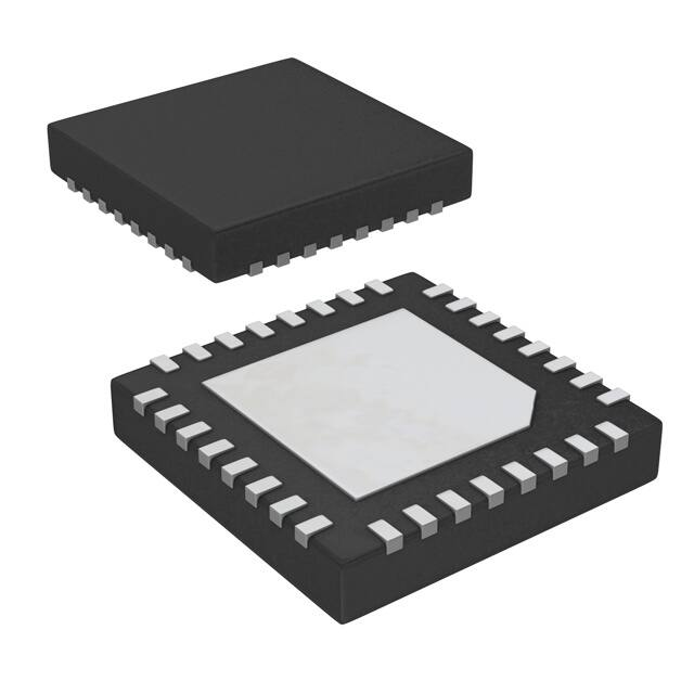


 工商网监
湘ICP备2023018690号
工商网监
湘ICP备2023018690号
