Datasheet
RL78/G23
R01DS0395EJ0121
Rev.1.21
Nov 15, 2022
RENESAS MCU
True low-power platform, 41-µA/MHz operating current, 210-nA holding current for 4 KB of RAM, up to
768-KB code flash memory and 48-KB RAM, Capacitive sensing unit, from 30 to 128 pins, 1.6-5.5 V
1. Outline
1.1
Features
Ultra-low power consumption technology
High-speed on-chip oscillator
• VDD = single power supply voltage of 1.6 to 5.5 V
• Select from 32 MHz, 24 MHz, 16 MHz, 12 MHz,
• HALT mode
• STOP mode
High-speed wakeup from the STOP mode is
8 MHz, 6 MHz, 4 MHz, 3 MHz, 2 MHz, or 1 MHz
• High accuracy:
±1.0% (VDD = 1.8 to 5.5 V, TA = -20 to +85°C)
possible.
• SNOOZE mode
Middle-speed on-chip oscillator
• Select from 4 MHz, 2 MHz, or 1 MHz (with
RL78 CPU core
adjustability)
• CISC architecture with 3-stage pipeline
• Minimum instruction execution time: Can be
changed from high speed (0.03125 µs @ 32 MHz
Low-speed on-chip oscillator
• 32.768 kHz (typ.) (with adjustability)
operation with the high-speed on-chip oscillator
clock) to ultra-low speed (30.5 µs @ 32.768 kHz
Operating ambient temperature
operation with the subsystem clock)
• TA = -40 to +85°C (2D: Consumer applications)
• Multiply/divide/multiply & accumulate instructions
• TA = -40 to +105°C (3C: Industrial applications)
are supported.
• Address space: 1 MB
Power management and reset function
• General-purpose registers:
• On-chip power-on-reset (POR) circuit
(8-bit register × 8) × 4 banks
• On-chip voltage detectors (LVD0 and LVD1)
• On-chip RAM: 12 to 48 KB
Data transfer controller (DTC)
Code flash memory
• Code flash memory: 96 to 768 KB
• Transfer modes: Normal transfer mode,
repeat transfer mode, block transfer mode
• Block size: 2 KB
• Activation sources: Activated by interrupt sources.
• Prohibition of block erase and rewriting
• Chain transfer function
(security function)
• On-chip debugging
SNOOZE mode sequencer (SMS)
• Self-programming
• Calculations and comparison of values by the
(with boot swapping and flash shield window)
commands for use in processing by the
sequencer can realize intermittent operations
Data flash memory
where the RL78/G23 does not have to return to
• Data flash memory: 8 KB
normal operation.
• Background operation (BGO):
Instructions can be executed from the program
memory while rewriting the data flash memory.
• Number of rewrites: 1,000,000 times (typ.)
• Sequentially handling a total of 32 processes with
the use of desired commands from among 21
different ones
• The SNOOZE mode sequencer offers operation
with low power consumption without using the
CPU, flash memory, and RAM.
R01DS0395EJ0121 Rev.1.21
Nov 15, 2022
Page 1 of 169
�RL78/G23
1. Outline
Logic and event link controller (ELCL)
Comparator
• Event signals can be set up between specified
• 2 channels
• Operating modes: Comparator high-speed mode
peripheral functions.
• The signals can be generated by the input of
multiple event signals to the logic circuit.
• Flip-flop circuits are incorporated to handle setting
Capacitive sensing unit
Serial interface
(CSINote 1):
3 to 8 channels
• UART/UART (LIN-bus supported)/UARTA:
I2C/Simplified I2C:
• CTSU2L operating voltage condition:
VDD = 1.8 to 5.5 V
• Self-capacitance method: A single pin configures
3 to 6 channels
•
reference voltage or D/A converter output are
selectable as the reference voltage.
and resetting functions.
• Simplified SPI
and comparator low-speed mode
• The external reference voltage and the internal
4 to 10 channels
a single key, supporting up to 32 keys
• Mutual capacitance method: Matrix configuration
Remote control signal receiver
with 8 × 8 pins, supporting up to 64 keys
• 1 channel
• Matching of 4 waveform patterns
(header, data 0, data 1, and special data)
Input/output port pins
• Number of port pins:
26 to 120 (N-ch open drain I/O
Timers
[withstand voltage of 6 V]: 2 to 4,
• 16-bit timer: 8 to 16 channels
N-ch open drain I/O [VDD withstand
• 32-bit interval timer:
voltage Note 2/EVDD withstand
1 channel in 32-bit counter mode
voltageNote 3]: 10 to 33,
2 channels in 16-bit counter mode
output current control pins: 6 to 8)
4 channels in 8-bit counter mode
• Realtime clock:
1 channel (counting of one second to 99 years,
alarm interrupt, and clock correction)
• Watchdog timer:
• Can be set to N-ch open drain or TTL input buffer,
and use of an on-chip pull-up resistor can be
specified.
• Connectable to a device with different voltage
(1.8, 2.5, or 3 V)
1 channel (operates with the dedicated low-speed
on-chip oscillator clock)
Others
• BCD (binary-coded decimal) correction circuit
A/D converter
• Key interrupt input
• 8-/10-/12-bit resolution A/D converter
• Clock output/buzzer output controller
• Analog input: 8 to 26 channels
• Internal reference voltage (1.48 V) and
Note 1.
Although the CSI function is generally
called SPI, it is also called CSI in this
temperature sensor
product, so it is referred to as such in
this manual.
D/A converter
• 8-bit resolution D/A converter
Note 2.
products.
• Analog output: 2 channels
• Output voltage: 0 V to VDD
This applies to the 30- to 52-pin
Note 3.
This applies to the 64- to 128-pin
products.
• Realtime output function
Remark
The functions mounted depend on the
product. See 1.6 Outline of
Functions.
R01DS0395EJ0121 Rev.1.21
Nov 15, 2022
Page 2 of 169
�RL78/G23
1. Outline
Ο ROM, RAM capacities
Flash
ROM
Data
flash
RL78/G23
RAM
30 pins
32 pins
36 pins
40 pins
44 pins
48 pins
768 KB
8 KB
48 KB
—
—
—
—
R7F100GFN
R7F100GGN
512 KB
8 KB
48 KB
—
—
—
—
R7F100GFL
R7F100GGL
384 KB
8 KB
32 KB
—
—
—
—
R7F100GFK
R7F100GGK
256 KB
8 KB
24 KB
R7F100GAJ
R7F100GBJ
R7F100GCJ
R7F100GEJ
R7F100GFJ
R7F100GGJ
192 KB
8 KB
20 KB
R7F100GAH
R7F100GBH
R7F100GCH
R7F100GEH
R7F100GFH
R7F100GGH
128 KB
8 KB
16 KB
R7F100GAG
R7F100GBG
R7F100GCG
R7F100GEG
R7F100GFG
R7F100GGG
96 KB
8 KB
12 KB
R7F100GAF
R7F100GBF
R7F100GCF
R7F100GEF
R7F100GFF
R7F100GGF
100 pins
128 pins
Flash
ROM
Data
flash
RAM
RL78/G23
52 pins
64 pins
80 pins
768 KB
8 KB
48 KB
R7F100GJN
R7F100GLN
R7F100GMN
R7F100GPN
R7F100GSN
512 KB
8 KB
48 KB
R7F100GJL
R7F100GLL
R7F100GML
R7F100GPL
R7F100GSL
384 KB
8 KB
32 KB
R7F100GJK
R7F100GLK
R7F100GMK
R7F100GPK
R7F100GSK
256 KB
8 KB
24 KB
R7F100GJJ
R7F100GLJ
R7F100GMJ
R7F100GPJ
R7F100GSJ
192 KB
8 KB
20 KB
R7F100GJH
R7F100GLH
R7F100GMH
R7F100GPH
—
128 KB
8 KB
16 KB
R7F100GJG
R7F100GLG
R7F100GMG
R7F100GPG
—
96 KB
8 KB
12 KB
R7F100GJF
R7F100GLF
—
—
—
R01DS0395EJ0121 Rev.1.21
Nov 15, 2022
Page 3 of 169
�RL78/G23
1.2
1. Outline
List of Part Numbers
Figure 1 - 1
Part Number, Memory Size, and Package of RL78/G23
Product name
Ordering part number
R 7 F 1 0 0 G L J 3 x x x C F B # AA0
Packaging specification
#BA0, #AA0: Tray (LFQFP, LQFP, LSSOP, HWQFN)
#BC0, #AC0: Tray (WFLGA)
#HA0: Embossed tape (LFQFP, LQFP, LSSOP, HWQFN)
#HC0: Embossed tape (WFLGA)
Package type
SP: LSSOP, 0.65-mm pitch
FP: LQFP, 0.80-mm pitch
FA: LQFP, 0.65-mm pitch
FB: LFQFP, 0.50-mm pitch
NP: HWQFN, 0.50-mm pitch
LA: WFLGA, 0.50-mm pitch
Fields of application
C: Industrial applications
D: Consumer applications
ROM number (omitted with blank products)
Ambient operating temperature range
2: -40 to +85°C
3: -40 to +105°C
ROM capacity
F: 96 KB
G: 128 KB
H: 192 KB
J: 256 KB
K: 384 KB
L: 512 KB
N: 768 KB
Pin count
A: 30 pins
B: 32 pins
C: 36 pins
E: 40 pins
F: 44 pins
G: 48 pins
J: 52 pins
L: 64 pins
M: 80 pins
P: 100 pins
S: 128 pins
RL78/G23
Device type
F: Flash memory
Renesas MCU
Renesas semiconductor product
R01DS0395EJ0121 Rev.1.21
Nov 15, 2022
Page 4 of 169
�RL78/G23
Table 1 - 1
Pin count
1. Outline
List of Ordering Part Numbers (1/3)
Package
Fields of
Application
Note
30
32
36
40
44
48
Product Name
30-pin plastic LSSOP
C
(7.62 mm (300), 0.65-mm pitch)
R7F100GAF3CSP, R7F100GAG3CSP,
R7F100GAH3CSP, R7F100GAJ3CSP
D
R7F100GAF2DSP, R7F100GAG2DSP,
R7F100GAH2DSP, R7F100GAJ2DSP
C
R7F100GBF3CNP, R7F100GBG3CNP,
R7F100GBH3CNP, R7F100GBJ3CNP
D
R7F100GBF2DNP, R7F100GBG2DNP,
R7F100GBH2DNP, R7F100GBJ2DNP
C
R7F100GBF3CFP, R7F100GBG3CFP,
R7F100GBH3CFP, R7F100GBJ3CFP
D
R7F100GBF2DFP, R7F100GBG2DFP,
R7F100GBH2DFP, R7F100GBJ2DFP
C
R7F100GCF3CLA, R7F100GCG3CLA,
R7F100GCH3CLA, R7F100GCJ3CLA
D
R7F100GCF2DLA, R7F100GCG2DLA,
R7F100GCH2DLA, R7F100GCJ2DLA
C
R7F100GEF3CNP, R7F100GEG3CNP,
R7F100GEH3CNP, R7F100GEJ3CNP
D
R7F100GEF2DNP, R7F100GEG2DNP,
R7F100GEH2DNP, R7F100GEJ2DNP
C
R7F100GFF3CFP, R7F100GFG3CFP,
R7F100GFH3CFP, R7F100GFJ3CFP,
R7F100GFK3CFP, R7F100GFL3CFP,
R7F100GFN3CFP
D
R7F100GFF2DFP, R7F100GFG2DFP,
R7F100GFH2DFP, R7F100GFJ2DFP,
R7F100GFK2DFP, R7F100GFL2DFP,
R7F100GFN2DFP
C
R7F100GGF3CFB, R7F100GGG3CFB,
R7F100GGH3CFB, R7F100GGJ3CFB,
R7F100GGK3CFB, R7F100GGL3CFB,
R7F100GGN3CFB
D
R7F100GGF2DFB, R7F100GGG2DFB,
R7F100GGH2DFB, R7F100GGJ2DFB,
R7F100GGK2DFB, R7F100GGL2DFB,
R7F100GGN2DFB
C
R7F100GGF3CNP, R7F100GGG3CNP,
R7F100GGH3CNP, R7F100GGJ3CNP,
R7F100GGK3CNP, R7F100GGL3CNP,
R7F100GGN3CNP
D
R7F100GGF2DNP, R7F100GGG2DNP,
R7F100GGH2DNP, R7F100GGJ2DNP,
R7F100GGK2DNP, R7F100GGL2DNP,
R7F100GGN2DNP
32-pin plastic HWQFN
(5 × 5 mm, 0.5-mm pitch)
32-pin plastic LQFP
(7 × 7 mm, 0.80-mm pitch)
Ordering Part Number
36-pin plastic WFLGA
(4 × 4 mm, 0.50-mm pitch)
40-pin plastic HWQFN
(6 × 6 mm, 0.50-mm pitch)
44-pin plastic LQFP
(10 × 10 mm, 0.80-mm pitch)
48-pin plastic LFQFP
(7 × 7 mm, 0.50-mm pitch)
48-pin plastic HWQFN
(7 × 7 mm, 0.50-mm pitch)
R01DS0395EJ0121 Rev.1.21
Nov 15, 2022
Packaging
Specification
Renesas Code
#AA0, #BA0,
#HA0
PLSP0030JB-B
#AA0, #BA0,
#HA0
PWQN0032KE-A
#AA0, #BA0,
#HA0
PLQP0032GB-A
#BC0, #AC0, PWLG0036KB-A
#HC0
#AA0, #BA0,
#HA0
PWQN0040KD-A
#AA0, #BA0,
#HA0
PLQP0044GC-A
#AA0, #BA0,
#HA0
PLQP0048KB-B
#AA0, #BA0,
#HA0
PWQN0048KC-A
Page 5 of 169
�RL78/G23
Table 1 - 1
Pin count
1. Outline
List of Ordering Part Numbers (2/3)
Package
Fields of
Application
Ordering Part Number
Product Name
Note
52
64
52-pin plastic LQFP
(10 × 10 mm, 0.65-mm pitch)
64-pin plastic LQFP
(12 × 12 mm, 0.65-mm pitch)
64-pin plastic LFQFP
(10 × 10 mm, 0.50-mm pitch)
64-pin plastic WFLGA
(5 × 5 mm, 0.50-mm pitch)
80
80-pin plastic LQFP
(14 × 14 mm, 0.65-mm pitch)
80-pin plastic LFQFP
(12 × 12 mm, 0.50-mm pitch)
R01DS0395EJ0121 Rev.1.21
Nov 15, 2022
C
R7F100GJF3CFA, R7F100GJG3CFA,
R7F100GJH3CFA, R7F100GJJ3CFA,
R7F100GJK3CFA, R7F100GJL3CFA,
R7F100GJN3CFA
D
R7F100GJF2DFA, R7F100GJG2DFA,
R7F100GJH2DFA, R7F100GJJ2DFA,
R7F100GJK2DFA, R7F100GJL2DFA,
R7F100GJN2DFA
C
R7F100GLF3CFA, R7F100GLG3CFA,
R7F100GLH3CFA, R7F100GLJ3CFA,
R7F100GLK3CFA, R7F100GLL3CFA,
R7F100GLN3CFA
D
R7F100GLF2DFA, R7F100GLG2DFA,
R7F100GLH2DFA, R7F100GLJ2DFA,
R7F100GLK2DFA, R7F100GLL2DFA,
R7F100GLN2DFA
C
R7F100GLF3CFB, R7F100GLG3CFB,
R7F100GLH3CFB, R7F100GLJ3CFB,
R7F100GLK3CFB, R7F100GLL3CFB,
R7F100GLN3CFB
D
R7F100GLF2DFB, R7F100GLG2DFB,
R7F100GLH2DFB, R7F100GLJ2DFB,
R7F100GLK2DFB, R7F100GLL2DFB,
R7F100GLN2DFB
C
R7F100GLF3CLA, R7F100GLG3CLA,
R7F100GLH3CLA, R7F100GLJ3CLA,
R7F100GLK3CLA, R7F100GLL3CLA,
R7F100GLN3CLA
D
R7F100GLF2DLA, R7F100GLG2DLA,
R7F100GLH2DLA, R7F100GLJ2DLA,
R7F100GLK2DLA, R7F100GLL2DLA,
R7F100GLN2DLA
C
R7F100GMG3CFA, R7F100GMH3CFA,
R7F100GMJ3CFA, R7F100GMK3CFA,
R7F100GML3CFA, R7F100GMN3CFA
D
R7F100GMG2DFA, R7F100GMH2DFA,
R7F100GMJ2DFA, R7F100GMK2DFA,
R7F100GML2DFA, R7F100GMN2DFA
C
R7F100GMG3CFB, R7F100GMH3CFB,
R7F100GMJ3CFB, R7F100GMK3CFB,
R7F100GML3CFB, R7F100GMN3CFB
D
R7F100GMG2DFB, R7F100GMH2DFB,
R7F100GMJ2DFB, R7F100GMK2DFB,
R7F100GML2DFB, R7F100GMN2DFB
Packaging
Specification
Renesas Code
#AA0, #BA0,
#HA0
PLQP0052JA-A
#AA0, #BA0,
#HA0
PLQP0064JA-A
#AA0, #BA0,
#HA0
PLQP0064KB-C
#BC0, #AC0, PWLG0064KB-A
#HC0
#AA0, #BA0,
#HA0
PLQP0080JA-B
#AA0, #BA0,
#HA0
PLQP0080KB-B
Page 6 of 169
�RL78/G23
Table 1 - 1
Pin count
1. Outline
List of Ordering Part Numbers (3/3)
Package
Fields of
Application
Ordering Part Number
Product Name
Note
100
100-pin plastic LFQFP
(14 × 14 mm, 0.50-mm pitch)
100-pin plastic LQFP
(14 × 20 mm, 0.65-mm pitch)
128
Note
128-pin plastic LFQFP
(14 × 20 mm, 0.50-mm pitch)
C
R7F100GPG3CFB, R7F100GPH3CFB,
R7F100GPJ3CFB, R7F100GPK3CFB,
R7F100GPL3CFB, R7F100GPN3CFB
D
R7F100GPG2DFB, R7F100GPH2DFB,
R7F100GPJ2DFB, R7F100GPK2DFB,
R7F100GPL2DFB, R7F100GPN2DFB
C
R7F100GPG3CFA, R7F100GPH3CFA,
R7F100GPJ3CFA, R7F100GPK3CFA,
R7F100GPL3CFA, R7F100GPN3CFA
D
R7F100GPG2DFA, R7F100GPH2DFA,
R7F100GPJ2DFA, R7F100GPK2DFA,
R7F100GPL2DFA, R7F100GPN2DFA
C
R7F100GSJ3CFB, R7F100GSK3CFB,
R7F100GSL3CFB, R7F100GSN3CFB
D
R7F100GSJ2DFB, R7F100GSK2DFB,
R7F100GSL2DFB, R7F100GSN2DFB
Packaging
Specification
Renesas Code
#AA0, #BA0,
#HA0
PLQP0100KB-B
#AA0, #BA0,
#HA0
PLQP0100JC-A
#AA0, #BA0,
#HA0
PLQP0128KD-A
For the fields of application, see Figure 1 - 1 Part Number, Memory Size, and Package of RL78/G23.
R01DS0395EJ0121 Rev.1.21
Nov 15, 2022
Page 7 of 169
�RL78/G23
1.3
1. Outline
Pin Configuration (Top View)
1.3.1
30-pin products
• 30-pin plastic LSSOP (7.62 mm (300), 0.65-mm pitch)
Note
1
2
3
4
5
6
7
8
9
10
11
12
13
14
15
RL78/G23
(Top View)
P20/ANI0/AVREFP/EI20
P01/ANI16/TS27Note/EI01/EO01/TO00/RxD1
P00/ANI17/TS26Note/EI00/TI00/TxD1
P120/ANI19/IVCMP1/EI120
P40/TOOL0
RESET
P137/EI137/INTP0
P122/X2/EXCLK/XT2/EXCLKS/EI122
P121/X1/XT1/EI121
REGC
VSS
VDD
P60/EO60/CCD04/SCLA0
P61/EO61/CCD05/SDAA0
P31/TS01/EI31/TI03/TO03/INTP4/PCLBUZ0
30
29
28
27
26
25
24
23
22
21
20
19
18
17
16
P21/ANI1/AVREFM/EI21
P22/ANI2/ANO0/TS20Note/EI22
P23/ANI3/ANO1/IVREF0/TS21Note/EI23
P147/ANI18/IVCMP0/EI147
P10/EI10/EO10/SCK00/SCL00/(TI07)/(TO07)
P11/EI11/EO11/SI00/RxD0/TOOLRxD/SDA00/(TI06)/(TO06)
P12/EI12/EO12/SO00/TxD0/TOOLTxD/(TI05)/(TO05)
P13/IVREF1/EO13/TxD2/SO20/(SDAA0)/(TI04)/(TO04)
P14/VCOUT1/EO14/RxD2/SI20/SDA20/(SCLA0)/(TI03)/(TO03)
P15/EO15/PCLBUZ1/SCK20/SCL20/(TI02)/(TO02)
P16/EO16/CCD00/TI01/TO01/INTP5/(RxD0)
P17/EO17/CCD01/TI02/TO02/(TxD0)
P51/EI51/EO51/CCD02/INTP2/SO11
P50/TS00/EI50/EO50/CCD03/INTP1/SI11/SDA11
P30/VCOUT0/TSCAP/EI30/INTP3/RTC1HZ/SCK11/SCL11
Not present in products with 128 or fewer Kbytes of code flash memory.
Caution
Connect the REGC pin to VSS via a capacitor (0.47 to 1 µF).
Remark 1.
For pin identification, see 1.4 Pin Identification.
Remark 2. Functions in parentheses in the above figure can be assigned via settings in the peripheral I/O redirection register
(PIOR). Refer to Figure 4 - 10 Format of Peripheral I/O Redirection Register (PIOR) in the RL78/G23 User's Manual.
R01DS0395EJ0121 Rev.1.21
Nov 15, 2022
Page 8 of 169
�Remote control signal receiver
(REMC)
Communications Interfaces
Serial interface UARTA
(UARTA)
Timer array unit
(TAU)
Timers
Capacitive sensing unit
(CTSU2L)
Key interrupt
(KR)
HMIs
Interrupt
(INTP)
Comparator
(CMP)
D/A converter
(DAC)
A/D converter
(ADC)
Power supply, system clock,
and debugging
ELCL input/output port
Digital port
Output current control port
Analog Circuits
Serial interface IICA
(IICA)
I/O
Serial array unit
(SAU)
Multiplexed Pin Functions of the 30-pin Products (1/2)
Realtime Clock
(RTC)
Table 1 - 2
30LSSOP
1. Outline
Pin
Number
RL78/G23
1
P20
—
EI20
—
ANI0/
—
AVREFP
—
—
—
—
—
—
—
—
—
—
2
P01
—
EI01/
EO01
—
ANI16
—
—
—
TS27
TO00
—
RxD1
—
—
—
EI00
—
TI00
—
TxD1
—
—
—
3
P00
—
—
Note
ANI17
—
—
—
—
TS26
Note
4
P120
—
EI120
—
ANI19
—
IVCMP1 —
—
—
—
—
—
—
—
—
5
P40
—
—
TOOL0
—
—
—
—
—
—
—
—
—
—
—
6
—
—
—
RESET
7
P137
—
EI137
8
P122
—
EI122
9
P121
—
10
—
—
—
—
—
—
—
—
—
—
—
—
—
—
—
—
—
INTP0
—
—
—
—
—
—
—
—
X2/XT2/
EXCLK/
EXCLKS
—
—
—
—
—
—
—
—
—
—
—
—
EI121
X1/XT1
—
—
—
—
—
—
—
—
—
—
—
—
—
—
REGC
—
—
—
—
—
—
—
—
—
—
—
—
11
—
—
—
VSS
—
—
—
—
—
—
—
—
—
—
—
—
12
—
—
—
VDD
—
—
—
—
—
—
—
—
—
—
—
—
13
P60
CCD04
EO60
—
—
—
—
—
—
—
—
—
—
SCLA0
—
—
14
P61
CCD05
EO61
—
—
—
—
—
—
—
—
—
—
SDAA0
—
—
15
P31
—
EI31
PCLBUZ0
—
—
—
INTP4
—
TS01
TI03/
TO03
—
—
—
—
—
16
P30
—
EI30
—
—
—
VCOUT0 INTP3
—
TSCAP
—
RTC1HZ SCK11/
SCL11
—
—
—
17
P50
CCD03
EI50/
EO50
—
—
—
—
INTP1
—
TS00
—
—
SI11/
SDA11
—
—
—
18
P51
CCD02
EI51/
EO51
—
—
—
—
INTP2
—
—
—
—
SO11
—
—
—
19
P17
CCD01
EO17
—
—
—
—
—
—
TI02/
TO02
—
(TxD0)
—
—
—
20
P16
CCD00
EO16
—
—
—
—
INTP5
—
—
TI01/
TO01
—
(RxD0)
—
—
—
21
P15
—
EO15
PCLBUZ1
—
—
—
—
—
—
(TI02)/
(TO02)
—
SCK20/ —
SCL20
—
—
22
P14
—
EO14
—
—
—
VCOUT1 —
—
—
(TI03)/
(TO03)
—
SI20/
RxD2/
SDA20
(SCLA0) —
—
23
P13
—
EO13
—
—
—
IVREF1 —
—
—
(TI04)/
(TO04)
—
SO20/
TxD2
(SDAA0) —
—
24
P12
—
EI12/
EO12
TOOLTxD
—
—
—
—
—
—
(TI05)/
(TO05)
—
SO00/
TxD0
—
—
—
25
P11
—
EI11/
EO11
TOOLRxD
—
—
—
—
—
—
(TI06)/(
TO06)
—
SI00/
RxD0/
SDA00
—
—
—
26
P10
—
EI10/
EO10
—
—
—
—
—
—
—
(TI07)/
(TO07)
—
SCK00/ —
SCL00
—
—
R01DS0395EJ0121 Rev.1.21
Nov 15, 2022
Page 9 of 169
�Remote control signal receiver
(REMC)
Serial interface UARTA
(UARTA)
Communications Interfaces
Serial interface IICA
(IICA)
Timer array unit
(TAU)
Timers
Capacitive sensing unit
(CTSU2L)
Key interrupt
(KR)
Comparator
(CMP)
D/A converter
(DAC)
A/D converter
(ADC)
HMIs
27
P147
—
EI147
—
ANI18
—
IVCMP0 —
—
—
—
—
—
—
—
—
28
P23
—
EI23
—
ANI3
ANO1
IVREF0 —
—
TS21
—
—
—
—
—
—
—
—
—
—
—
—
—
—
—
—
—
—
Interrupt
(INTP)
Digital port
ELCL input/output port
Power supply, system clock,
and debugging
Analog Circuits
Serial array unit
(SAU)
I/O
Realtime Clock
(RTC)
Multiplexed Pin Functions of the 30-pin Products (2/2)
Output current control port
Table 1 - 2
30LSSOP
1. Outline
Pin
Number
RL78/G23
Note
29
P22
—
EI22
—
ANI2
ANO0
—
—
—
TS20
Note
30
P21
Note
—
EI21
—
—
ANI1/
AVREFM
—
—
—
—
Not present in products with 128 or fewer Kbytes of code flash memory.
R01DS0395EJ0121 Rev.1.21
Nov 15, 2022
Page 10 of 169
�RL78/G23
1.3.2
1. Outline
32-pin products
• 32-pin plastic HWQFN (5 × 5 mm, 0.50-mm pitch)
P10/EI10/EO10/SCK00/SCL00/(TI07)/(TO07)
P11/EI11/EO11/SI00/RxD0/TOOLRxD/SDA00/(TI06)/(TO06)
P12/EI12/EO12/SO00/TxD0/TOOLTxD/(TI05)/(TO05)
P13/IVREF1/EO13/TxD2/SO20/(SDAA0)/(TI04)/(TO04)
P14/VCOUT1/EO14/RxD2/SI20/SDA20/(SCLA0)/(TI03)/(TO03)
P15/EO15/PCLBUZ1/SCK20/SCL20/(TI02)/(TO02)
P16/EO16/CCD00/TI01/TO01/INTP5/(RxD0)
P17/EO17/CCD01/TI02/TO02/(TxD0)
• 32-pin plastic LQFP (7 × 7 mm, 0.80-mm pitch)
Exposed die padNote 2
INDEX MARK
24 23 22 21 2019 18 17
25
16
26
15
27
14
RL78/G23
28
13
(Top
View)
29
12
30
11
31
10
32
9
1 2 3 4 5 6 7 8
P51/EI51/EO51/CCD02/INTP2/SO11
P50/TS00/EI50/EO50/CCD03/INTP1/SI11/SDA11
P30/VCOUT0/TSCAP/EI30/INTP3/RTC1HZ/SCK11/SCL11
P70/RIN0/TS02
P31/TS01/EI31/TI03/TO03/INTP4/PCLBUZ0
P62/CCD06
P61/EO61/CCD05/SDAA0
P60/EO60/CCD04/SCLA0
P40/TOOL0
RESET
P137/EI137/INTP0
P122/X2/EXCLK/XT2/EXCLKS/EI122
P121/X1/XT1/EI121
REGC
VSS
VDD
P147/ANI18/IVCMP0/EI147
P23/ANI3/ANO1/IVREF0/TS21Note 1/EI23
P22/ANI2/ANO0/TS20Note 1/EI22
P21/ANI1/AVREFM/EI21
P20/ANI0/AVREFP/EI20
Note 1
/EI01/EO01/TO00/RxD1
P01/ANI16/TS27
P00/ANI17/TS26Note 1/EI00/TI00/TxD1
P120/ANI19/IVCMP1/EI120
Note 1. Not present in products with 128 or fewer Kbytes of code flash memory.
Note 2. The 32-pin plastic LQFP (7 × 7 mm, 0.80-mm pitch) products do not have an exposed die pad.
Caution
Connect the REGC pin to VSS via a capacitor (0.47 to 1 µF).
Remark 1. For pin identification, see 1.4 Pin Identification.
Remark 2. Functions in parentheses in the above figure can be assigned via settings in the peripheral I/O redirection register
(PIOR). Refer to Figure 4 - 10 Format of Peripheral I/O Redirection Register (PIOR) in the RL78/G23 User's Manual.
Remark 3. It is recommended to connect an exposed die pad to VSS.
R01DS0395EJ0121 Rev.1.21
Nov 15, 2022
Page 11 of 169
�Remote control signal receiver
(REMC)
Communications Interfaces
Serial interface UARTA
(UARTA)
Timer array unit
(TAU)
Timers
Capacitive sensing unit
(CTSU2L)
Key interrupt
(KR)
HMIs
Interrupt
(INTP)
Comparator
(CMP)
D/A converter
(DAC)
A/D converter
(ADC)
Power supply, system clock,
and debugging
ELCL input/output port
Digital port
Output current control port
Analog Circuits
Serial interface IICA
(IICA)
I/O
Serial array unit
(SAU)
Multiplexed Pin Functions of the 32-pin Products (1/2)
Realtime Clock
(RTC)
Table 1 - 3
32HWQFN, 32LQFP
1. Outline
Pin
Number
RL78/G23
1
P40
—
—
TOOL0
—
—
—
—
—
—
—
—
—
—
—
—
2
—
—
—
RESET
—
—
—
—
—
—
—
—
—
—
—
—
3
P137
—
EI137
—
—
—
—
INTP0
—
—
—
—
—
—
—
—
4
P122
—
EI122
X2/XT2/
EXCLK/
EXCLKS
—
—
—
—
—
—
—
—
—
—
—
—
5
P121
—
EI121
X1/XT1
—
—
—
—
—
—
—
—
—
—
—
—
6
—
—
—
REGC
—
—
—
—
—
—
—
—
—
—
—
—
7
—
—
—
VSS
—
—
—
—
—
—
—
—
—
—
—
—
8
—
—
—
VDD
—
—
—
—
—
—
—
—
—
—
—
—
9
P60
CCD04
EO60
—
—
—
—
—
—
—
—
—
—
SCLA0
—
—
10
P61
CCD05
EO61
—
—
—
—
—
—
—
—
—
—
SDAA0
—
—
11
P62
CCD06
—
—
—
—
—
—
—
—
—
—
—
—
—
—
12
P31
—
EI31
PCLBUZ0
—
—
—
INTP4
—
TS01
TI03/
TO03
—
—
—
—
—
13
P70
—
—
—
—
—
—
—
—
TS02
—
—
—
—
—
RIN0
14
P30
—
EI30
—
—
—
VCOUT0 INTP3
—
TSCAP
—
RTC1HZ SCK11/
SCL11
—
—
—
15
P50
CCD03
EI50/
EO50
—
—
—
—
INTP1
—
TS00
—
—
SI11/
SDA11
—
—
—
16
P51
CCD02
EI51/
EO51
—
—
—
—
INTP2
—
—
—
—
SO11
—
—
—
17
P17
CCD01
EO17
—
—
—
—
—
—
—
TI02/
TO02
—
(TxD0)
—
—
—
18
P16
CCD00
EO16
—
—
—
—
INTP5
—
—
TI01/
TO01
—
(RxD0)
—
—
—
19
P15
—
EO15
PCLBUZ1
—
—
—
—
—
—
(TI02)/
(TO02)
—
SCK20/ —
SCL20
—
—
20
P14
—
EO14
—
—
—
VCOUT1 —
—
—
(TI03)/
(TO03)
—
SI20/
RxD2/
SDA20
(SCLA0) —
—
21
P13
—
EO13
—
—
—
IVREF1 —
—
—
(TI04)/
(TO04)
—
SO20/
TxD2
(SDAA0) —
—
22
P12
—
EI12/
EO12
TOOLTxD
—
—
—
—
—
—
(TI05)/
(TO05)
—
SO00/
TxD0
—
—
—
23
P11
—
EI11/
EO11
TOOLRxD
—
—
—
—
—
—
(TI06)/
(TO06)
—
SI00/
RxD0/
SDA00
—
—
—
24
P10
—
EI10/
EO10
—
—
—
—
—
—
—
(TI07)/
(TO07)
—
SCK00/ —
SCL00
—
—
25
P147
—
—
—
ANI18
—
IVCMP0 —
—
—
—
—
—
—
—
—
26
P23
—
EI23
—
ANI3
ANO1
IVREF0 —
—
TS21
—
—
—
—
—
—
Note
R01DS0395EJ0121 Rev.1.21
Nov 15, 2022
Page 12 of 169
�27
—
EI22
—
ANI2
ANO0
—
—
—
TS20
Remote control signal receiver
(REMC)
Serial interface UARTA
(UARTA)
Communications Interfaces
Serial interface IICA
(IICA)
Timer array unit
(TAU)
Timers
Capacitive sensing unit
(CTSU2L)
Key interrupt
(KR)
HMIs
Interrupt
(INTP)
Comparator
(CMP)
D/A converter
(DAC)
A/D converter
(ADC)
Power supply, system clock,
and debugging
ELCL input/output port
Digital port
P22
Analog Circuits
Serial array unit
(SAU)
I/O
Realtime Clock
(RTC)
Multiplexed Pin Functions of the 32-pin Products (2/2)
Output current control port
Table 1 - 3
32HWQFN, 32LQFP
1. Outline
Pin
Number
RL78/G23
—
—
—
—
—
—
Note
28
P21
—
EI21
—
—
ANI1/
AVREFM
—
—
—
—
—
—
—
—
—
—
29
P20
—
EI20
—
ANI0/
—
AVREFP
—
—
—
—
—
—
—
—
—
—
30
P01
—
EI01/
EO01
—
ANI16
—
—
—
TS27
TO00
—
RxD1
—
—
—
EI00
—
TI00
—
TxD1
—
—
—
—
—
—
—
—
—
31
P00
—
—
Note
ANI17
—
—
—
—
TS26
Note
32
P120
Note
—
EI120
—
ANI19
—
IVCMP1 —
—
—
Not present in products with 128 or fewer Kbytes of code flash memory.
R01DS0395EJ0121 Rev.1.21
Nov 15, 2022
Page 13 of 169
�RL78/G23
1.3.3
1. Outline
36-pin products
• 36-pin plastic WFLGA (4 × 4 mm, 0.50-mm pitch)
Top View
Bottom View
6
5
RL78/G23
4
(Top View)
3
2
1
A
B
C
D
E
F
F
E
D
C
B
A
INDEX MARK
A
6
P60/EO60/CCD04/
B
VDD
C
P121/X1/XT1/EI121
SCLA0
5
D
P122/X2/EXCLK/XT2/
E
P137/EI137/INTP0
P40/TOOL0
RESET
P120/ANI19/IVCMP1/
EXCLKS/EI122
P62/CCD06
P61/EO61/CCD05/SD
VSS
REGC
AA0
4
F
EI120
P72/TS04/SO21/
P71/TS03/SI21/
P14/VCOUT1/EO14/
P31/TS01/EI31/TI03/
P00/TS26Note/EI00/
P01/TS27Note/EI01/
TxDA0
SDA21/RxDA0
RxD2/SI20/SDA20/
TO03/INTP4/
TI00/TxD1
EO01/TO00/RxD1
(SCLA0)/(TI03)/
PCLBUZ0
(TO03)
3
P50/TS00/EI50/EO50/
P70/TS02/RIN0/
P15/EO15/PCLBUZ1/
P22/ANI2/ANO0/
P20/ANI0/AVREFP/
P21/ANI1/AVREFM/
CCD03/INTP1/SI11/
SCK21/SCL21
SCK20/SCL20/
TS20Note/EI22
EI20
EI21
P24/ANI4/TS22Note
P23/ANI3/ANO1/
(TI02)/(TO02)
SDA11
2
1
P30/VCOUT0/TSCAP/
P16/EO16/CCD00/
P12/EI12/EO12/SO00/
P11/EI11/EO11/SI00/
EI30/INTP3/RTC1HZ/
TI01/TO01/INTP5/
TxD0/TOOLTxD/
RxD0/TOOLRxD/
IVREF0/TS21Note/
SCK11/SCL11
(RxD0)
(TI05)/(TO05)
SDA00/(TI06)/(TO06)
EI23
P51/EI51/EO51/
P17/EO17/CCD01/
P13/IVREF1/EO13/
P10/EI10/EO10/
P147/ANI18/IVCMP0/
CCD02/INTP2/
TI02/TO02/(TxD0)
TxD2/SO20/(SDAA0)/
SCK00/SCL00/
EI147
(TI04)/(TO04)
(TI07)/(TO07)
SO11
Note
Caution
P25/ANI5/TS23Note
Not present in products with 128 or fewer Kbytes of code flash memory.
Connect the REGC pin to VSS via a capacitor (0.47 to 1 µF).
Remark 1. For pin identification, see 1.4 Pin Identification.
Remark 2. Functions in parentheses in the above figure can be assigned via settings in the peripheral I/O redirection register
(PIOR). Refer to Figure 4 - 10 Format of Peripheral I/O Redirection Register (PIOR) in the RL78/G23 User's Manual.
R01DS0395EJ0121 Rev.1.21
Nov 15, 2022
Page 14 of 169
�A1
P51
CCD02
EI51/
EO51
—
—
—
—
INTP2
—
—
—
—
A2
P30
—
EI30
—
—
—
VCOUT0 INTP3
—
TSCAP
—
A3
P50
CCD03
EI50/
EO50
—
—
—
—
INTP1
—
TS00
A4
P72
—
—
—
—
—
—
—
—
A5
P62
CCD06
—
—
—
—
—
—
A6
P60
CCD04
EO60
—
—
—
—
B1
P17
CCD01
EO17
—
—
—
—
B2
P16
CCD00
EO16
—
—
—
B3
P70
—
—
—
—
B4
P71
—
—
—
B5
P61
CCD05
EO61
—
B6
—
SO11
Remote control signal receiver
(REMC)
Communications Interfaces
Serial interface UARTA
(UARTA)
Timer array unit
(TAU)
Timers
Capacitive sensing unit
(CTSU2L)
Key interrupt
(KR)
HMIs
Interrupt
(INTP)
Comparator
(CMP)
D/A converter
(DAC)
A/D converter
(ADC)
Power supply, system clock,
and debugging
ELCL input/output port
Digital port
Output current control port
Analog Circuits
Serial interface IICA
(IICA)
I/O
Serial array unit
(SAU)
Multiplexed Pin Functions of the 36-pin Products (1/2)
Realtime Clock
(RTC)
Table 1 - 4
36WFLGA
1. Outline
Pin
Number
RL78/G23
—
—
—
RTC1HZ SCK11/
SCL11
—
—
—
—
—
SI11/
SDA11
—
—
—
TS04
—
—
SO21
—
TxDA0
—
—
—
—
—
—
—
—
—
—
—
—
—
—
—
SCLA0
—
—
—
—
—
TI02/
TO02
—
(TxD0)
—
—
—
—
INTP5
—
—
TI01/
TO01
—
(RxD0)
—
—
—
—
—
—
—
TS02
—
—
SCK21/ —
SCL21
—
RIN0
—
—
—
—
—
TS03
—
—
SI21/
SDA21
—
RxDA0
—
—
—
—
—
—
—
—
—
—
SDAA0
—
—
—
—
VDD
—
—
—
—
—
—
—
—
—
—
—
—
C1 P13
—
EO13
—
—
—
IVREF1 —
—
—
(TI04)/
(TO04)
—
SO20/
TxD2
(SDAA0) —
—
C2 P12
—
EI12/
EO12
TOOLTxD
—
—
—
—
—
—
(TI05)/
(TO05)
—
SO00/
TxD0
—
—
—
C3 P15
—
EO15
PCLBUZ1
—
—
—
—
—
—
(TI02)/
(TO02)
—
SCK20/ —
SCL20
—
—
C4 P14
—
EO14
—
—
—
VCOUT1 —
—
—
(TI03)/
(TO03)
—
SI20/
RxD2/
SDA20
(SCLA0) —
—
C5 —
—
—
Vss
—
—
—
—
—
—
—
—
—
—
—
—
C6 P121
—
EI121
X1/XT1
—
—
—
—
—
—
—
—
—
—
—
—
D1 P10
—
EI10/
EO10
—
—
—
—
—
—
—
(TI07)/
(TO07)
—
SCK00/ —
SCL00
—
—
D2 P11
—
EI11/
EO11
TOOLRxD
—
—
—
—
—
—
(TI06)/
(TO06)
—
SI00/
RxD0/
SDA00
—
—
—
D3 P22
—
EI22
—
ANI2
ANO0
—
—
—
TS20
—
—
—
—
—
—
Note
D4 P31
—
EI31
PCLBUZ0
—
—
—
INTP4
—
TS01
TI03/
TO03
—
—
—
—
—
D5 —
—
—
REGC
—
—
—
—
—
—
—
—
—
—
—
—
D6 P122
—
EI122
X2/XT2/
EXCLK/
EXCLKS
—
—
—
—
—
—
—
—
—
—
—
—
E1
—
EI147
—
ANI18
—
IVCMP0 —
—
—
—
—
—
—
—
—
P147
R01DS0395EJ0121 Rev.1.21
Nov 15, 2022
Page 15 of 169
�E2
—
—
—
ANI4
—
—
—
—
TS22
Remote control signal receiver
(REMC)
Communications Interfaces
Serial interface UARTA
(UARTA)
Timer array unit
(TAU)
Timers
Capacitive sensing unit
(CTSU2L)
Key interrupt
(KR)
HMIs
Interrupt
(INTP)
Comparator
(CMP)
D/A converter
(DAC)
A/D converter
(ADC)
Power supply, system clock,
and debugging
ELCL input/output port
Output current control port
Digital port
P24
Analog Circuits
Serial interface IICA
(IICA)
I/O
Serial array unit
(SAU)
Multiplexed Pin Functions of the 36-pin Products (2/2)
Realtime Clock
(RTC)
Table 1 - 4
36WFLGA
1. Outline
Pin
Number
RL78/G23
—
—
—
—
—
—
Note
E3
P20
—
EI20
—
—
ANI0/
AVREFP
—
—
—
—
—
—
—
—
—
—
E4
P00
—
EI00
—
—
—
—
—
TS26
TI00
—
TxD1
—
—
—
—
Note
E5
—
—
—
RESET
—
—
—
—
—
—
—
—
—
—
—
—
E6
P137
—
EI137
—
—
—
—
INTP0
—
—
—
—
—
—
—
—
F1
P25
—
—
—
ANI5
—
—
—
—
TS23
—
—
—
—
—
—
—
—
—
—
—
—
—
—
—
—
—
—
—
TS27
TO00
—
RxD1
—
—
—
Note
F2
P23
—
EI23
—
ANI3
ANO1
IVREF0 —
—
TS21
Note
F3
P21
—
EI21
—
—
ANI1/
AVREFM
—
—
—
F4
P01
—
EI01/
EO01
—
—
—
—
—
—
EI120
—
ANI19
—
IVCMP1 —
—
—
—
—
—
—
—
—
—
—
TOOL0
—
—
—
—
—
—
—
—
—
—
—
F5
P120
F6
P40
Note
—
Note
—
Not present in products with 128 or fewer Kbytes of code flash memory.
R01DS0395EJ0121 Rev.1.21
Nov 15, 2022
Page 16 of 169
�RL78/G23
1.3.4
1. Outline
40-pin products
P147/ANI18/IVCMP0/EI147
P10/EI10/EO10/SCK00/SCL00/(TI07)/(TO07)
P11/EI11/EO11/SI00/RxD0/TOOLRxD/SDA00/(TI06)/(TO06)
P12/EI12/EO12/SO00/TxD0/TOOLTxD/(TI05)/(TO05)
P13/IVREF1/EO13/TxD2/SO20/(SDAA0)/(TI04)/(TO04)
P14/VCOUT1/EO14/RxD2/SI20/SDA20/(SCLA0)/(TI03)/(TO03)
P15/EO15/PCLBUZ1/SCK20/SCL20/(TI02)/(TO02)
P16/EO16/CCD00/TI01/TO01/INTP5/(RxD0)
P17/EO17/CCD01/TI02/TO02/(TxD0)
P51/EI51/EO51/CCD02/INTP2/SO11
• 40-pin plastic HWQFN (6 × 6 mm, 0.50-mm pitch)
INDEX MARK
Note
Caution
30 29 28 27 26 25 24 23 22 21
31
20
32
19
Exposed die pad
33
18
34
17
RL78/G23
35
16
36
15
(Top View)
37
14
38
13
39
12
40
11
1 2 3 4 5 6 7 8 9 10
P50/TS00/EI50/EO50/CCD03/INTP1/SI11/SDA11
P30/VCOUT0/TSCAP/EI30/INTP3/RTC1HZ/SCK11/SCL11
P70/TS02/RIN0/KR0/SCK21/SCL21
P71/TS03/KR1/SI21/SDA21/RxDA0
P72/TS04/KR2/SO21/TxDA0
P73/TS05/KR3
P31/TS01/EI31/TI03/TO03/INTP4/PCLBUZ0
P62/CCD06
P61/EO61/CCD05/SDAA0
P60/EO60/CCD04/SCLA0
P40/TOOL0
RESET
P124/XT2/EXCLKS
P123/XT1
P137/EI137/INTP0
P122/X2/EXCLK/EI122
P121/X1/VBAT/EI121
REGC
VSS
VDD
P26/ANI6/TS24Note
P25/ANI5/TS23Note
P24/ANI4/TS22Note
P23/ANI3/ANO1/IVREF0/TS21Note/EI23
P22/ANI2/ANO0/TS20Note/EI22
P21/ANI1/AVREFM/EI21
P20/ANI0/AVREFP/EI20
Note
P01/TS27 /EI01/EO01/TO00/RxD1
P00/TS26Note/EI00/TI00/TxD1
P120/ANI19/IVCMP1/EI120
Not present in products with 128 or fewer Kbytes of code flash memory.
Connect the REGC pin to VSS via a capacitor (0.47 to 1 µF).
Remark 1. For pin identification, see 1.4 Pin Identification.
Remark 2. Functions in parentheses in the above figure can be assigned via settings in the peripheral I/O redirection register
(PIOR). Refer to Figure 4 - 10 Format of Peripheral I/O Redirection Register (PIOR) in the RL78/G23 User's Manual.
Remark 3. It is recommended to connect an exposed die pad to VSS.
R01DS0395EJ0121 Rev.1.21
Nov 15, 2022
Page 17 of 169
�Remote control signal receiver
(REMC)
Communications Interfaces
Serial interface UARTA
(UARTA)
Timer array unit
(TAU)
Timers
Capacitive sensing unit
(CTSU2L)
Key interrupt
(KR)
HMIs
Interrupt
(INTP)
Comparator
(CMP)
D/A converter
(DAC)
A/D converter
(ADC)
Power supply, system clock,
and debugging
ELCL input/output port
Digital port
Output current control port
Analog Circuits
Serial interface IICA
(IICA)
I/O
Serial array unit
(SAU)
Multiplexed Pin Functions of the 40-pin Products (1/2)
Realtime Clock
(RTC)
Table 1 - 5
40HWQFN
1. Outline
Pin
Number
RL78/G23
1
P40
—
—
TOOL0
—
—
—
—
—
—
—
—
—
—
—
—
2
—
—
—
RESET
—
—
—
—
—
—
—
—
—
—
—
—
3
P124
—
—
XT2/
EXCLKS
—
—
—
—
—
—
—
—
—
—
—
—
4
P123
—
—
XT1
—
—
—
—
—
—
—
—
—
—
—
—
5
P137
—
EI137
—
—
—
—
INTP0
—
—
—
—
—
—
—
—
6
P122
—
EI122
X2/EXCLK
—
—
—
—
—
—
—
—
—
—
—
—
7
P121
—
EI121
X1/VBAT
—
—
—
—
—
—
—
—
—
—
—
—
8
—
—
—
REGC
—
—
—
—
—
—
—
—
—
—
—
—
9
—
—
—
VSS
—
—
—
—
—
—
—
—
—
—
—
—
10
—
—
—
VDD
—
—
—
—
—
—
—
—
—
—
—
—
11
P60
CCD04
EO60
—
—
—
—
—
—
—
—
—
—
SCLA0
—
—
12
P61
CCD05
EO61
—
—
—
—
—
—
—
—
—
—
SDAA0
—
—
13
P62
CCD06
—
—
—
—
—
—
—
—
—
—
—
—
—
—
14
P31
—
EI31
PCLBUZ0
—
—
—
INTP4
—
TS01
TI03/
TO03
—
—
—
—
—
15
P73
—
—
—
—
—
—
—
KR3
TS05
—
—
—
—
—
—
16
P72
—
—
—
—
—
—
—
KR2
TS04
—
—
SO21
—
TxDA0
—
17
P71
—
—
—
—
—
—
—
KR1
TS03
—
—
SI21/
SDA21
—
RxDA0
—
18
P70
—
—
—
—
—
—
—
KR0
TS02
—
—
SCK21/ —
SCL21
—
RIN0
19
P30
—
EI30
—
—
—
VCOUT0 INTP3
—
TSCAP
—
RTC1HZ SCK11/
SCL11
—
—
—
20
P50
CCD03
EI50/
EO50
—
—
—
—
INTP1
—
TS00
—
—
SI11/
SDA11
—
—
—
21
P51
CCD02
EI51/
EO51
—
—
—
—
INTP2
—
—
—
—
SO11
—
—
—
22
P17
CCD01
EO17
—
—
—
—
—
—
—
TI02/
TO02
—
(TxD0)
—
—
—
23
P16
CCD00
EO16
—
—
—
—
INTP5
—
—
TI01/
TO01
—
(RxD0)
—
—
—
24
P15
—
EO15
PCLBUZ1
—
—
—
—
—
—
(TI02)/
(TO02)
—
SCK20/ —
SCL20
—
—
25
P14
—
EO14
—
—
—
VCOUT1 —
—
—
(TI03)/
(TO03)
—
SI20/
xD2/
SDA20
(SCLA0) —
—
26
P13
—
EO13
—
—
—
IVREF1 —
—
—
(TI04)/
(TO04)
—
SO20/
TxD2
(SDAA0) —
—
27
P12
—
EI12/
EO12
TOOLTxD
—
—
—
—
—
(TI05)/
(TO05)
—
SO00/
TxD0
—
—
28
P11
—
EI11/
EO11
TOOLRxD
—
—
—
—
—
(TI06)/
(TO06)
—
SI00/
RxD0/
SDA00
—
—
R01DS0395EJ0121 Rev.1.21
Nov 15, 2022
—
—
Page 18 of 169
�29
P10
—
EI10/
EO10
—
—
—
—
—
—
30
P147
—
EI147
—
ANI18
—
IVCMP0 —
—
31
P26
—
—
—
ANI6
—
—
—
—
—
TS24
Remote control signal receiver
(REMC)
Communications Interfaces
Serial interface UARTA
(UARTA)
Timer array unit
(TAU)
Timers
Capacitive sensing unit
(CTSU2L)
Key interrupt
(KR)
HMIs
Interrupt
(INTP)
Comparator
(CMP)
D/A converter
(DAC)
A/D converter
(ADC)
Power supply, system clock,
and debugging
ELCL input/output port
Digital port
Output current control port
Analog Circuits
Serial interface IICA
(IICA)
I/O
Serial array unit
(SAU)
Multiplexed Pin Functions of the 40-pin Products (2/2)
Realtime Clock
(RTC)
Table 1 - 5
40HWQFN
1. Outline
Pin
Number
RL78/G23
(TI07)/
(TO07)
—
SCK00/ —
SCL00
—
—
—
—
—
—
—
—
—
—
—
—
—
—
—
—
—
—
—
—
—
—
—
—
—
—
—
—
—
—
—
—
—
—
—
—
—
—
Note
32
P25
—
—
—
ANI5
—
—
—
—
TS23
Note
33
P24
—
—
—
ANI4
—
—
—
—
TS22
Note
34
P23
—
EI23
—
ANI3
ANO1
IVREF0 —
—
TS21
Note
35
P22
—
EI22
—
ANI2
ANO0
—
—
—
TS20
Note
36
P21
—
EI21
—
ANI1/
—
AVREFM
—
—
—
—
—
—
—
—
—
—
37
P20
—
EI20
—
ANI0/
—
AVREFP
—
—
—
—
—
—
—
—
—
—
38
P01
—
EI01/
EO01
—
—
—
—
—
TS27
TO00
—
RxD1
—
—
—
EI00
—
TI00
—
TxD1
—
—
—
—
—
—
—
—
—
39
P00
—
—
Note
—
—
—
—
—
TS26
Note
40
P120
Note
—
EI120
—
ANI19
—
IVCMP1 —
—
—
Not present in products with 128 or fewer Kbytes of code flash memory.
R01DS0395EJ0121 Rev.1.21
Nov 15, 2022
Page 19 of 169
�RL78/G23
1.3.5
1. Outline
44-pin products
P147/ANI18/IVCMP0/EI147
P146
P10/EI10/EO10/SCK00/SCL00/(TI07)/(TO07)
P11/EI11/EO11/SI00/RxD0/TOOLRxD/SDA00/(TI06)/(TO06)
P12/EI12/EO12/SO00/TxD0/TOOLTxD/(TI05)/(TO05)
P13/IVREF1/EO13/TxD2/SO20/(SDAA0)/(TI04)/(TO04)
P14/VCOUT1/EO14/RxD2/SI20/SDA20/(SCLA0)/(TI03)/(TO03)
P15/EO15/PCLBUZ1/SCK20/SCL20/(TI02)/(TO02)
P16/EO16/CCD00/TI01/TO01/INTP5/(RxD0)
P17/EO17/CCD01/TI02/TO02/(TxD0)
P51/EI51/EO51/CCD02/INTP2/SO11
• 44-pin plastic LQFP (10 × 10 mm, 0.80-mm pitch)
34
35
36
37
38
39
40
41
42
43
44
33 32 31 30 29 28 27 26 25 24 23
22
21
20
19
RL78/G23
18
17
(Top View)
16
15
14
13
12
1 2 3 4 5 6 7 8 9 10 11
P50/TS00/EI50/EO50/INTP1/SI11/SDA11
P30/VCOUT0/TSCAP/EI30/INTP3/RTC1HZ/SCK11/SCL11
P70/TS02/RIN0/KR0/SCK21/SCL21
P71/TS03/KR1/SI21/SDA21/RxDA0
P72/TS04/KR2/SO21/TxDA0
P73/TS05/KR3
P31/TS01/EI31/TI03/TO03/INTP4/PCLBUZ0
P63/CCD07/SDAA1
P62/CCD06/SCLA1
P61/EO61/CCD05/SDAA0
P60/EO60/CCD04/SCLA0
P41/RxDA1/TI07/TO07
P40/TOOL0
RESET
P124/XT2/EXCLKS
P123/XT1
P137/EI137/INTP0
P122/X2/EXCLK/EI122
P121/X1/VBAT/EI121
REGC
VSS
VDD
P27/ANI7/TS25Note
P26/ANI6/TS24Note
P25/ANI5/TS23Note
P24/ANI4/TS22Note
P23/ANI3/ANO1/IVREF0/TS21Note/EI23
P22/ANI2/ANO0/TS20Note/EI22
P21/ANI1/AVREFM/EI21
P20/ANI0/AVREFP/EI20
Note
P01/TS27 /EI01/EO01/TO00/RxD1
P00/TS26Note/EI00/TI00/TxD1
P120/ANI19/IVCMP1/TxDA1/EI120
Note
Caution
Not present in products with 128 or fewer Kbytes of code flash memory.
Connect the REGC pin to VSS via a capacitor (0.47 to 1 µF).
Remark 1. For pin identification, see 1.4 Pin Identification.
Remark 2. Functions in parentheses in the above figure can be assigned via settings in the peripheral I/O redirection register
(PIOR). Refer to Figure 4 - 10 Format of Peripheral I/O Redirection Register (PIOR) in the RL78/G23 User's Manual.
R01DS0395EJ0121 Rev.1.21
Nov 15, 2022
Page 20 of 169
�Remote control signal receiver
(REMC)
Communications Interfaces
Serial interface UARTA
(UARTA)
Timer array unit
(TAU)
Timers
Capacitive sensing unit
(CTSU2L)
Key interrupt
(KR)
HMIs
Interrupt
(INTP)
Comparator
(CMP)
D/A converter
(DAC)
A/D converter
(ADC)
Power supply, system clock,
and debugging
ELCL input/output port
Digital port
Output current control port
Analog Circuits
Serial interface IICA
(IICA)
I/O
Serial array unit
(SAU)
Multiplexed Pin Functions of the 44-pin Products (1/2)
Realtime Clock
(RTC)
Table 1 - 6
44LQFP
1. Outline
Pin
Number
RL78/G23
1
P41
—
—
—
—
—
—
—
—
—
TI07/
TO07
—
—
—
RxDA1
—
2
P40
—
—
TOOL0
—
—
—
—
—
—
—
—
—
—
—
—
3
—
—
RESET
—
—
—
—
—
—
—
—
—
—
—
—
4
P124
—
—
XT2/
EXCLKS
—
—
—
—
—
—
—
—
—
—
—
—
5
P123
—
—
XT1
—
—
—
—
—
—
—
—
—
—
—
—
6
P137
—
EI137
—
—
—
—
INTP0
—
—
—
—
—
—
—
—
7
P122
—
EI122
X2/EXCLK
—
—
—
—
—
—
—
—
—
—
—
—
8
P121
—
EI121
X1/VBAT
—
—
—
—
—
—
—
—
—
—
—
—
9
—
—
—
REGC
—
—
—
—
—
—
—
—
—
—
—
—
10
—
—
—
VSS
—
—
—
—
—
—
—
—
—
—
—
—
11
—
—
—
VDD
—
—
—
—
—
—
—
—
—
—
—
—
12
P60
CCD04
EO60
—
—
—
—
—
—
—
—
—
—
SCLA0
—
—
13
P61
CCD05
EO61
—
—
—
—
—
—
—
—
—
—
SDAA0
—
—
14
P62
CCD06
—
—
—
—
—
—
—
—
—
—
—
SCLA1
—
—
15
P63
CCD07
—
—
—
—
—
—
—
—
—
—
—
SDAA1
—
—
16
P31
—
EI31
PCLBUZ0
—
—
—
INTP4
—
TS01
TI03/
TO03
—
—
—
—
—
17
P73
—
—
—
—
—
—
—
KR3
TS05
—
—
—
—
—
—
18
P72
—
—
—
—
—
—
—
KR2
TS04
—
—
SO21
—
TxDA0
—
19
P71
—
—
—
—
—
—
—
KR1
TS03
—
—
SI21/
SDA21
—
RxDA0
—
20
P70
—
—
—
—
—
—
—
KR0
TS02
—
—
SCK21/ —
SCL21
—
RIN0
21
P30
—
EI30
—
—
—
VCOUT0 INTP3
—
TSCAP
—
RTC1HZ SCK11/
SCL11
—
—
—
22
P50
—
EI50/
EO50
—
—
—
—
INTP1
—
TS00
—
—
SI11/
SDA11
—
—
—
23
P51
CCD02
EI51/
EO51
—
—
—
—
INTP2
—
—
—
—
SO11
—
—
—
24
P17
CCD01
EO17
—
—
—
—
—
—
TI02/
TO02
—
(TxD0)
—
—
—
25
P16
CCD00
EO16
—
—
—
—
INTP5
—
—
TI01/
TO01
—
(RxD0)
—
—
—
26
P15
—
EO15
PCLBUZ1
—
—
—
—
—
—
(TI02)/
(TO02)
—
SCK20/ —
SCL20
—
—
27
P14
—
EO14
—
—
—
VCOUT1 —
—
—
(TI03)/
(TO03)
—
SI20/
RxD2/
SDA20
(SCLA0) —
—
28
P13
—
EO13
—
—
—
IVREF1 —
—
—
(TI04)/
(TO04)
—
SO20/
TxD2
(SDAA0) —
—
R01DS0395EJ0121 Rev.1.21
Nov 15, 2022
Page 21 of 169
�Remote control signal receiver
(REMC)
Communications Interfaces
Serial interface UARTA
(UARTA)
Timer array unit
(TAU)
Timers
Capacitive sensing unit
(CTSU2L)
Key interrupt
(KR)
HMIs
Interrupt
(INTP)
Comparator
(CMP)
D/A converter
(DAC)
A/D converter
(ADC)
Power supply, system clock,
and debugging
ELCL input/output port
Digital port
Output current control port
Analog Circuits
Serial interface IICA
(IICA)
I/O
Serial array unit
(SAU)
Multiplexed Pin Functions of the 44-pin Products (2/2)
Realtime Clock
(RTC)
Table 1 - 6
44LQFP
1. Outline
Pin
Number
RL78/G23
29
P12
—
EI12/
EO12
TOOLTxD
—
—
—
—
—
—
(TI05)/
(TO05)
—
SO00/
TxD0
—
—
—
30
P11
—
EI11/
EO11
TOOLRxD
—
—
—
—
—
—
(TI06)/
(TO06)
—
SI00/
RxD0/
SDA00
—
—
—
31
P10
—
EI10/
EO10
—
—
—
—
—
—
—
(TI07)/
(TO07)
—
SCK00/ —
SCL00
—
—
32
P146
—
—
—
—
—
—
—
—
—
—
—
—
—
—
—
33
P147
—
EI147
—
ANI18
—
IVCMP0 —
—
—
—
—
—
—
—
—
34
P27
—
—
—
ANI7
—
—
—
TS25
—
—
—
—
—
—
—
—
—
—
—
—
—
—
—
—
—
—
—
—
—
—
—
—
—
—
—
—
—
—
—
—
—
—
—
—
—
Note
35
P26
—
—
—
ANI6
—
—
—
—
TS24
Note
36
P25
—
—
—
ANI5
—
—
—
—
TS23
Note
37
P24
—
—
—
ANI4
—
—
—
—
TS22
Note
38
P23
—
EI23
—
ANI3
ANO1
IVREF0 —
—
TS21
Note
39
P22
—
EI22
—
ANI2
ANO0
—
—
—
TS20
Note
40
P21
—
EI21
—
—
ANI1/
AVREFM
—
—
—
—
—
—
—
—
—
—
41
P20
—
EI20
—
ANI0/
—
AVREFP
—
—
—
—
—
—
—
—
—
—
42
P01
—
EI01/
EO01
—
—
—
—
—
TS27
TO00
—
RxD1
—
—
—
EI00
—
TI00
—
TxD1
—
—
—
—
—
—
—
TxDA1
—
43
P00
—
—
Note
—
—
—
—
—
TS26
Note
44
P120
Note
—
EI120
—
ANI19
—
IVCMP1 —
—
—
Not present in products with 128 or fewer Kbytes of code flash memory.
R01DS0395EJ0121 Rev.1.21
Nov 15, 2022
Page 22 of 169
�RL78/G23
1.3.6
1. Outline
48-pin products
• 48-pin plastic LFQFP (7 × 7 mm, 0.50-mm pitch)
P140/PCLBUZ0/INTP6
P00/TS26Note 1/EI00/TI00/TxD1
P01/TS27Note 1/EI01/EO01/TO00/RxD1
P130
P20/ANI0/AVREFP/EI20
P21/ANI1/AVREFM/EI21
P22/ANI2/ANO0/TS20Note 1/EI22
P23/ANI3/ANO1/IVREF0/TS21Note 1/EI23
P24/ANI4/TS22Note 1
P25/ANI5/TS23Note 1
P26/ANI6/TS24Note 1
P27/ANI7/TS25Note 1
• 48-pin plastic HWQFN (7 × 7 mm, 0.50-mm pitch)
Exposed die padNote 2
36 35 34 33 32 31 30 29 28 27 26 25
24
37
23
38
22
39
21
40
20
41
RL78/G23
19
42
18
43
(Top View)
17
44
16
45
15
46
14
47
13
48
1 2 3 4 5 6 7 8 9 10 11 12
P147/ANI18/IVCMP0/EI147
P146
P10/EI10/EO10/SCK00/SCL00/(TI07)/(TO07)
P11/EI11/EO11/SI00/RxD0/TOOLRxD/SDA00/(TI06)/(TO06)
P12/EI12/EO12/SO00/TxD0/TOOLTxD/(TI05)/(TO05)
P13/IVREF1/EO13/TxD2/SO20/(SDAA0)/(TI04)/(TO04)
P14/VCOUT1/EO14/RxD2/SI20/SDA20/(SCLA0)/(TI03)/(TO03)
P15/EO15/PCLBUZ1/SCK20/SCL20/(TI02)/(TO02)
P16/EO16/CCD00/TI01/TO01/INTP5/(RxD0)
P17/EO17/CCD01/TI02/TO02/(TxD0)
P51/EI51/EO51/CCD02/INTP2/SO11
P50/TS00/EI50/EO50/CCD03/INTP1/SI11/SDA11
P60/EO60/CCD04/SCLA0
P61/EO61/CCD05/SDAA0
P62/CCD06/SCLA1
P63/CCD07/SDAA1
P31/TS01/EI31/TI03/TO03/INTP4/(PCLBUZ0)
P75/TS07/KR5/INTP9/SCK01/SCL01
P74/TS06/KR4/INTP8/SI01/SDA01
P73/TS05/KR3/SO01
P72/TS04/KR2/SO21/TxDA0
P71/TS03/KR1/SI21/SDA21/RxDA0
P70/TS02/RIN0/KR0/SCK21/SCL21
P30/VCOUT0/TSCAP/EI30/INTP3/RTC1HZ/SCK11/SCL11
P120/ANI19/IVCMP1/TxDA1/EI120
P41/RxDA1/TI07/TO07
P40/TOOL0
RESET
P124/XT2/EXCLKS
P123/XT1
P137/EI137/INTP0
P122/X2/EXCLK/EI122
P121/X1/VBAT/EI121
REGC
VSS
VDD
Note 1. Not present in products with 128 or fewer Kbytes of code flash memory.
Note 2. The 48-pin plastic LFQFP (7 × 7 mm, 0.50-mm pitch) products do not have an exposed die pad.
Caution
Connect the REGC pin to VSS via a capacitor (0.47 to 1 µF).
Remark 1. For pin identification, see 1.4 Pin Identification.
Remark 2. Functions in parentheses in the above figure can be assigned via settings in the peripheral I/O redirection register
(PIOR). Refer to Figure 4 - 10 Format of Peripheral I/O Redirection Register (PIOR) in the RL78/G23 User's Manual.
Remark 3. It is recommended to connect an exposed die pad to VSS.
R01DS0395EJ0121 Rev.1.21
Nov 15, 2022
Page 23 of 169
�Remote control signal receiver
(REMC)
Communications Interfaces
Serial interface UARTA
(UARTA)
Timer array unit
(TAU)
Timers
Capacitive sensing unit
(CTSU2L)
Key interrupt
(KR)
HMIs
Interrupt
(INTP)
Comparator
(CMP)
D/A converter
(DAC)
A/D converter
(ADC)
Power supply, system clock,
and debugging
ELCL input/output port
Digital port
Output current control port
Analog Circuits
Serial interface IICA
(IICA)
I/O
Serial array unit
(SAU)
Multiplexed Pin Functions of the 48-pin Products (1/2)
Realtime Clock
(RTC)
Table 1 - 7
48LFQFP, 48HWQFN
1. Outline
Pin
Number
RL78/G23
1
P60
CCD04
EO60
—
—
—
—
—
—
—
—
—
—
SCLA0
—
—
2
P61
CCD05
EO61
—
—
—
—
—
—
—
—
—
—
SDAA0
—
—
3
P62
CCD06
—
—
—
—
—
—
—
—
—
—
—
SCLA1
—
—
4
P63
CCD07
—
—
—
—
—
—
—
—
—
—
—
SDAA1
—
—
5
P31
—
EI31
(PCLBUZ0) —
—
—
INTP4
—
TS01
TI03/
TO03
—
—
—
—
—
6
P75
—
—
—
—
—
—
INTP9
KR5
TS07
—
—
SCK01/ —
SCL01
—
—
7
P74
—
—
—
—
—
—
INTP8
KR4
TS06
—
—
SI01/
SDA01
—
—
—
8
P73
—
—
—
—
—
—
—
KR3
TS05
—
—
SO01
—
—
—
9
P72
—
—
—
—
—
—
—
KR2
TS04
—
—
SO21
—
TxDA0
—
10
P71
—
—
—
—
—
—
—
KR1
TS03
—
—
SI21/
SDA21
—
RxDA0
—
11
P70
—
—
—
—
—
—
—
KR0
TS02
—
—
SCK21/ —
SCL21
—
RIN0
12
P30
—
EI30
—
—
—
VCOUT0 INTP3
—
TSCAP
—
RTC1HZ SCK11/
SCL11
—
—
—
13
P50
CCD03
EI50/
EO50
—
—
—
—
INTP1
—
TS00
—
—
SI11/
SDA11
—
—
—
14
P51
CCD02
EI51/
EO51
—
—
—
—
INTP2
—
—
—
—
SO11
—
—
—
15
P17
CCD01
EO17
—
—
—
—
—
—
—
TI02/
TO02
—
(TxD0)
—
—
—
16
P16
CCD00
EO16
—
—
—
—
INTP5
—
—
TI01/
TO01
—
(RxD0)
—
—
—
17
P15
—
EO15
PCLBUZ1
—
—
—
—
—
—
(TI02)/
(TO02)
—
SCK20/ —
SCL20
—
—
18
P14
—
EO14
—
—
—
VCOUT1 —
—
—
(TI03)/
(TO03)
—
SI20/
RxD2/
SDA20
(SCLA0) —
—
19
P13
—
EO13
—
—
—
IVREF1 —
—
—
(TI04)/
(TO04)
—
SO20/
TxD2
(SDAA0) —
—
20
P12
—
EI12/
EO12
TOOLTxD
—
—
—
—
—
—
(TI05)/
(TO05)
—
SO00/
TxD0
—
—
—
21
P11
—
EI11/
EO11
TOOLRxD
—
—
—
—
—
—
(TI06)/
(TO06)
—
SI00/
RxD0/
SDA00
—
—
—
22
P10
—
EI10/
EO10
—
—
—
—
—
—
—
(TI07)/
(TO07)
—
SCK00/ —
SCL00
—
—
23
P146
—
—
—
—
—
—
—
—
—
—
—
—
—
—
—
24
P147
—
EI147
—
ANI18
—
IVCMP0 —
—
—
—
—
—
—
—
—
25
P27
—
—
—
ANI7
—
—
—
TS25
—
—
—
—
—
—
—
Note
R01DS0395EJ0121 Rev.1.21
Nov 15, 2022
Page 24 of 169
�26
—
—
—
ANI6
—
—
—
—
TS24
Remote control signal receiver
(REMC)
Communications Interfaces
Serial interface UARTA
(UARTA)
Timer array unit
(TAU)
Timers
Capacitive sensing unit
(CTSU2L)
Key interrupt
(KR)
HMIs
Interrupt
(INTP)
Comparator
(CMP)
D/A converter
(DAC)
A/D converter
(ADC)
Power supply, system clock,
and debugging
ELCL input/output port
Output current control port
Digital port
P26
Analog Circuits
Serial interface IICA
(IICA)
I/O
Serial array unit
(SAU)
Multiplexed Pin Functions of the 48-pin Products (2/2)
Realtime Clock
(RTC)
Table 1 - 7
48LFQFP, 48HWQFN
1. Outline
Pin
Number
RL78/G23
—
—
—
—
—
—
—
—
—
—
—
—
—
—
—
—
—
—
—
—
—
—
—
—
—
—
—
—
—
—
Note
27
P25
—
—
—
ANI5
—
—
—
—
TS23
Note
28
P24
—
—
—
ANI4
—
—
—
—
TS22
Note
29
P23
—
EI23
—
ANI3
ANO1
IVREF0 —
—
TS21
Note
30
P22
—
EI22
—
ANI2
ANO0
—
—
—
TS20
Note
31
P21
—
EI21
—
—
ANI1/
AVREFM
—
—
—
—
—
—
—
—
—
—
32
P20
—
EI20
—
ANI0/
—
AVREFP
—
—
—
—
—
—
—
—
—
—
33
P130
—
—
—
—
—
—
—
—
—
—
—
—
—
—
—
34
P01
—
EI01/
EO01
—
—
—
—
—
—
TS27
TO00
—
RxD1
—
—
—
EI00
—
TI00
—
TxD1
—
—
—
35
P00
—
Note
—
—
—
—
—
TS26
Note
36
P140
—
—
PCLBUZ0
—
—
—
37
P120
—
EI120
—
ANI19
—
38
P41
—
—
—
—
39
P40
—
—
TOOL0
40
—
—
—
RESET
41
P124
—
—
42
P123
—
43
P137
44
P122
45
46
INTP6
—
—
—
—
—
—
—
—
IVCMP1 —
—
—
—
—
—
—
TxDA1
—
—
—
—
—
—
TI07/
TO07
—
—
—
RxDA1
—
—
—
—
—
—
—
—
—
—
—
—
—
—
—
—
—
—
—
—
—
—
—
—
—
XT2/
EXCLKS
—
—
—
—
—
—
—
—
—
—
—
—
—
XT1
—
—
—
—
—
—
—
—
—
—
—
—
—
EI137
—
—
—
—
INTP0
—
—
—
—
—
—
—
—
—
EI122
X2/EXCLK
—
—
—
—
—
—
—
—
—
—
—
—
P121
—
EI121
X1/VBAT
—
—
—
—
—
—
—
—
—
—
—
—
—
—
—
REGC
—
—
—
—
—
—
—
—
—
—
—
—
47
—
—
—
VSS
—
—
—
—
—
—
—
—
—
—
—
—
48
—
—
—
VDD
—
—
—
—
—
—
—
—
—
—
—
—
Note
Not present in products with 128 or fewer Kbytes of code flash memory.
R01DS0395EJ0121 Rev.1.21
Nov 15, 2022
Page 25 of 169
�RL78/G23
1.3.7
1. Outline
52-pin products
P30/VCOUT0/TSCAP/EI30/INTP3/RTC1HZ/SCK11/SCL11
P50/TS00/EI50/EO50/CCD03/INTP1/SI11/SDA11
P51/EI51/EO51/CCD02/INTP2/SO11
P17/EO17/CCD01/TI02/TO02/(TxD0)
P16/EO16/CCD00/TI01/TO01/INTP5/(RxD0)
P15/EO15/PCLBUZ1/SCK20/SCL20/(TI02)/(TO02)
P14/VCOUT1/EO14/RxD2/SI20/SDA20/(SCLA0)/(TI03)/(TO03)
P13/IVREF1/EO13/TxD2/SO20/(SDAA0)/(TI04)/(TO04)
P12/EI12/EO12/SO00/TxD0/TOOLTxD/(TI05)/(TO05)
P11/EI11/EO11/SI00/RxD0/TOOLRxD/SDA00/(TI06)/(TO06)
P10/EI10/EO10/SCK00/SCL00/(TI07)/(TO07)
P146
P147/ANI18/IVCMP0/EI147
• 52-pin plastic LQFP (10 × 10 mm, 0.65-mm pitch)
39 38 37 36 35 34 33 32 31 30 29 28 27
P27/ANI7/TS25Note
40
26
P70/TS02/RIN0/KR0/SCK21/SCL21
P26/ANI6/TS24Note
41
25
P71/TS03/KR1/SI21/SDA21/RxDA0
P25/ANI5/TS23Note
42
24
P72/TS04/KR2/SO21/TxDA0
P24/ANI4/TS22Note
43
23
P73/TS05/KR3/SO01
/EI23
44
22
P74/TS06/KR4/INTP8/SI01/SDA01
P22/ANI2/ANO0/TS20Note/EI22
45
21
P75/TS07/KR5/INTP9/SCK01/SCL01
P21/ANI1/AVREFM/EI21
46
20
P76/TS08/KR6/INTP10/(RxD2)
P20/ANI0/AVREFP/EI20
47
19
P77/TS09/KR7/INTP11/(TxD2)
P130
P03/ANI16/TS29Note/RxD1
48
18
P31/TS01/EI31/TI03/TO03/INTP4/(PCLBUZ0)
49
17
P63/CCD07/SDAA1
P02/ANI17/TS28Note/TxD1
50
16
P62/CCD06/SCLA1
P01/TS27Note/EI01/EO01/TO00
51
15
P61/EO61/CCD05/SDAA0
P00/TS26Note/EI00/TI00
52
14
P60/EO60/CCD04/SCLA0
Note
Caution
6
7 8
9 10 11 12 13
P40/TOOL0
RESET
P124/XT2/EXCLKS
P123/XT1
P122/X2/EXCLK/EI122
VDD
5
VSS
4
REGC
3
P121/X1/VBAT/EI121
2
P137/EI137/INTP0
1
P41/RxDA1/TI07/TO07
RL78/G23
(Top View)
P140/PCLBUZ0/INTP6
P23/ANI3/ANO1/IVREF0/TS21
P120/ANI19/IVCMP1/TxDA1/EI120
Note
Not present in products with 128 or fewer Kbytes of code flash memory.
Connect the REGC pin to VSS via a capacitor (0.47 to 1 µF).
Remark 1. For pin identification, see 1.4 Pin Identification.
Remark 2. Functions in parentheses in the above figure can be assigned via settings in the peripheral I/O redirection register
(PIOR). Refer to Figure 4 - 10 Format of Peripheral I/O Redirection Register (PIOR) in the RL78/G23 User's Manual.
R01DS0395EJ0121 Rev.1.21
Nov 15, 2022
Page 26 of 169
�—
—
—
2
P120
—
EI120
—
ANI19
—
3
P41
—
—
—
—
4
P40
—
—
TOOL0
—
INTP6
Remote control signal receiver
(REMC)
PCLBUZ0
Communications Interfaces
Serial interface UARTA
(UARTA)
—
Timer array unit
(TAU)
—
Timers
Capacitive sensing unit
(CTSU2L)
P140
Key interrupt
(KR)
1
HMIs
Interrupt
(INTP)
Comparator
(CMP)
D/A converter
(DAC)
A/D converter
(ADC)
Power supply, system clock,
and debugging
Digital port
ELCL input/output port
Output current control port
Analog Circuits
Serial interface IICA
(IICA)
I/O
Serial array unit
(SAU)
Multiplexed Pin Functions of the 52-pin Products (1/2)
Realtime Clock
(RTC)
Table 1 - 8
52LFQFP
1. Outline
Pin
Number
RL78/G23
—
—
—
—
—
—
—
—
IVCMP1 —
—
—
—
—
—
—
TxDA1
—
—
—
—
—
—
TI07/
TO07
—
—
—
RxDA1
—
—
—
—
—
—
—
—
—
—
—
—
5
—
—
—
RESET
—
—
—
—
—
—
—
—
—
—
—
—
6
P124
—
—
XT2/
EXCLKS
—
—
—
—
—
—
—
—
—
—
—
—
7
P123
—
—
XT1
—
—
—
—
—
—
—
—
—
—
—
—
8
P137
—
EI137
—
—
—
—
INTP0
—
—
—
—
—
—
—
—
9
P122
—
EI122
X2/EXCLK
—
—
—
—
—
—
—
—
—
—
—
—
10
P121
—
EI121
X1/VBAT
—
—
—
—
—
—
—
—
—
—
—
—
11
—
—
—
REGC
—
—
—
—
—
—
—
—
—
—
—
—
12
—
—
—
VSS
—
—
—
—
—
—
—
—
—
—
—
—
13
—
—
—
VDD
—
—
—
—
—
—
—
—
—
—
—
—
14
P60
CCD04
EO60
—
—
—
—
—
—
—
—
—
—
SCLA0
—
—
15
P61
CCD05
EO61
—
—
—
—
—
—
—
—
—
—
SDAA0
—
—
16
P62
CCD06
—
—
—
—
—
—
—
—
—
—
—
SCLA1
—
—
17
P63
CCD07
—
—
—
—
—
—
—
—
—
—
—
SDAA1
—
—
18
P31
—
EI31
(PCLBUZ0) —
—
—
INTP4
—
TS01
TI03/
TO03
—
—
—
—
—
19
P77
—
—
—
—
—
—
INTP11
KR7
TS09
—
—
(TxD2)
—
—
—
20
P76
—
—
—
—
—
—
INTP10 KR6
TS08
—
—
(RxD2)
—
—
—
21
P75
—
—
—
—
—
—
INTP9
KR5
TS07
—
—
SCK01/ —
SCL01
—
—
22
P74
—
—
—
—
—
—
INTP8
KR4
TS06
—
—
SI01/
SDA01
—
—
—
23
P73
—
—
—
—
—
—
—
KR3
TS05
—
—
SO01
—
—
—
24
P72
—
—
—
—
—
—
—
KR2
TS04
—
—
SO21
—
TxDA0
—
25
P71
—
—
—
—
—
—
—
KR1
TS03
—
—
SI21/
SDA21
—
RxDA0
—
26
P70
—
—
—
—
—
—
—
KR0
TS02
—
—
SCK21/ —
SCL21
—
RIN0
27
P30
—
EI30
—
—
—
VCOUT0 INTP3
—
TSCAP
—
RTC1HZ SCK11/
SCL11
—
—
—
28
P50
CCD03
EI50/
EO50
—
—
—
—
INTP1
—
TS00
—
—
SI11/
SDA11
—
—
—
29
P51
CCD02
EI51/
EO51
—
—
—
—
INTP2
—
—
—
—
SO11
—
—
—
30
P17
CCD01
EO17
—
—
—
—
—
—
—
TI02/
TO02
—
(TxD0)
—
—
—
R01DS0395EJ0121 Rev.1.21
Nov 15, 2022
Page 27 of 169
�Remote control signal receiver
(REMC)
Communications Interfaces
Serial interface UARTA
(UARTA)
Timer array unit
(TAU)
Timers
Capacitive sensing unit
(CTSU2L)
Key interrupt
(KR)
HMIs
Interrupt
(INTP)
Comparator
(CMP)
D/A converter
(DAC)
A/D converter
(ADC)
Power supply, system clock,
and debugging
ELCL input/output port
Digital port
Output current control port
Analog Circuits
Serial interface IICA
(IICA)
I/O
Serial array unit
(SAU)
Multiplexed Pin Functions of the 52-pin Products (2/2)
Realtime Clock
(RTC)
Table 1 - 8
52LFQFP
1. Outline
Pin
Number
RL78/G23
31
P16
CCD00
EO16
—
—
—
—
INTP5
—
—
TI01/
TO01
—
(RxD0)
—
—
—
32
P15
—
EO15
PCLBUZ1
—
—
—
—
—
—
(TI02)/
(TO02)
—
SCK20/ —
SCL20
—
—
33
P14
—
EO14
—
—
—
VCOUT1 —
—
—
(TI03)/
(TO03)
—
SI20/
RxD2/
SDA20
(SCLA0) —
—
34
P13
—
EO13
—
—
—
IVREF1 —
—
—
(TI04)/
(TO04)
—
SO20/
TxD2
(SDAA0) —
—
35
P12
—
EI12/
EO12
TOOLTxD
—
—
—
—
—
—
(TI05)/
(TO05)
—
SO00/
TxD0
—
—
—
36
P11
—
EI11/
EO11
TOOLRxD
—
—
—
—
—
—
(TI06)/
(TO06)
—
SI00/
RxD0/
SDA00
—
—
—
37
P10
—
EI10/
EO10
—
—
—
—
—
—
—
(TI07)/
(TO07)
—
SCK00/ —
SCL00
—
—
38
P146
—
—
—
—
—
—
—
—
—
—
—
—
—
—
—
39
P147
—
EI147
—
ANI18
—
IVCMP0 —
—
—
—
—
—
—
—
—
40
P27
—
—
—
ANI7
—
—
—
TS25
—
—
—
—
—
—
—
—
—
—
—
—
—
—
—
—
—
—
—
—
—
—
—
—
—
—
—
—
—
—
—
—
—
—
—
—
—
Note
41
P26
—
—
—
ANI6
—
—
—
—
TS24
Note
42
P25
—
—
—
ANI5
—
—
—
—
TS23
Note
43
P24
—
—
—
ANI4
—
—
—
—
TS22
Note
44
P23
—
EI23
—
ANI3
ANO1
IVREF0 —
—
TS21
Note
45
P22
—
EI22
—
ANI2
ANO0
—
—
—
TS20
Note
46
P21
—
EI21
—
—
ANI1/
AVREFM
—
—
—
—
—
—
—
—
—
—
47
P20
—
EI20
—
ANI0/
—
AVREFP
—
—
—
—
—
—
—
—
—
—
48
P130
—
—
—
—
—
—
—
—
—
—
—
—
—
—
—
49
P03
—
—
—
ANI16
—
—
—
—
TS29
—
—
RxD1
—
—
—
—
—
TxD1
—
—
—
TO00
—
—
—
—
—
TI00
—
—
—
—
—
Note
50
P02
—
—
—
ANI17
—
—
—
—
TS28
Note
51
52
P01
P00
—
—
EI01/
EO01
—
EI00
—
—
—
—
—
—
TS27
Note
—
—
—
—
—
TS26
Note
Note
Not present in products with 128 or fewer Kbytes of code flash memory.
R01DS0395EJ0121 Rev.1.21
Nov 15, 2022
Page 28 of 169
�RL78/G23
1.3.8
1. Outline
64-pin products
• 64-pin plastic LQFP (12 × 12 mm, 0.65-mm pitch)
P50/TS00/EI50/EO50/CCD03/INTP1/SI11/SDA11
P51/EI51/EO51/CCD02/INTP2/SO11
P52/(INTP10)
P53/(INTP11)
P54
P55/(PCLBUZ1)/(SCK00)
P17/EO17/CCD01/TI02/TO02/(SO00)/(TxD0)
P16/EO16/CCD00/TI01/TO01/INTP5/(SI00)/(RxD0)
P15/EO15/SCK20/SCL20/(TI02)/(TO02)
P14/VCOUT1/EO14/RxD2/SI20/SDA20/(SCLA0)/(TI03)/(TO03)
P13/IVREF1/EO13/TxD2/SO20/(SDAA0)/(TI04)/(TO04)
P12/EI12/EO12/SO00/TxD0/TOOLTxD/(INTP5)/(TI05)/(TO05)
P11/EI11/EO11/SI00/RxD0/TOOLRxD/SDA00/(TI06)/(TO06)
P10/EI10/EO10/SCK00/SCL00/(TI07)/(TO07)
P146
P147/ANI18/IVCMP0/EI147
• 64-pin plastic LFQFP (10 × 10 mm, 0.50-mm pitch)
48 47 46 45 44 43 42 41 40 39 38 37 36 35 34 33
P27/ANI7/TS25Note
P26/ANI6/TS24Note
P25/ANI5/TS23
Note
P24/ANI4/TS22
Note
P23/ANI3/ANO1/IVREF0/TS21
Note
/EI23
P22/ANI2/ANO0/TS20
Note
/EI22
P21/ANI1/AVREFM/EI21
P20/ANI0/AVREFP/EI20
P130
P04/SCK10/SCL10
P03/ANI16/TS29Note/SI10/RxD1/SDA10
P02/ANI17/TS28Note/SO10/TxD1
P01/TS27Note/EI01/EO01/TO00
P00/TS26Note/EI00/TI00
P141/PCLBUZ1/INTP7
P140/PCLBUZ0/INTP6
49
50
51
52
53
54
55
56
57
58
59
60
61
62
63
64
32
31
30
29
28
27
26
25
24
23
22
21
20
19
18
17
RL78/G23
(Top View)
P30/VCOUT0/TSCAP/EI30/INTP3/RTC1HZ/SCK11/SCL11
P05/TS10/TI05/TO05
P06/TS11/TI06/TO06/CLKA0
P70/TS02/RIN0/KR0/SCK21/SCL21
P71/TS03/KR1/SI21/SDA21/RxDA0
P72/TS04/KR2/SO21/TxDA0
P73/TS05/KR3/SO01
P74/TS06/KR4/INTP8/SI01/SDA01
P75/TS07/KR5/INTP9/SCK01/SCL01
P76/TS08/KR6/INTP10/(RxD2)
P77/TS09/KR7/INTP11/(TxD2)
P31/TS01/EI31/TI03/TO03/INTP4/(PCLBUZ0)
P63/CCD07/SDAA1
P62/CCD06/SCLA1
P61/EO61/CCD05/SDAA0
P60/EO60/CCD04/SCLA0
Note
EVDD0
VDD
VSS
EVSS0
REGC
P121/X1/VBAT/EI121
P122/X2/EXCLK/EI122
P137/EI137/INTP0
P123/XT1
P124/XT2/EXCLKS
RESET
P40/TOOL0
P41/RxDA1/TI07/TO07
P42/TxDA1/TI04/TO04
P43/CLKA1
P120/ANI19/IVCMP1/EI120
1 2 3 4 5 6 7 8 9 10 11 12 13 14 15 16
Not present in products with 128 or fewer Kbytes of code flash memory.
Caution 1. Connect the EVSS0 pin to the same ground as the VSS pin.
Caution 2. Make sure that the voltage on the VDD pin is no less than that on the EVDD0 pin.
Caution 3. Connect the REGC pin to VSS via a capacitor (0.47 to 1 µF).
Remark 1. For pin identification, see 1.4 Pin Identification.
Remark 2. When using the microcontroller for an application where the noise generated inside the microcontroller must be reduced,
it is recommended to supply separate powers to the VDD and EVDD0 pins and connect the VSS and EVSS0 pins to
separate ground lines.
Remark 3. Functions in parentheses in the above figure can be assigned via settings in the peripheral I/O redirection register
(PIOR). Refer to Figure 4 - 10 Format of Peripheral I/O Redirection Register (PIOR) in the RL78/G23 User's Manual.
R01DS0395EJ0121 Rev.1.21
Nov 15, 2022
Page 29 of 169
�Timers
Capacitive sensing unit
(CTSU2L)
Power supply, system clock,
and debugging
HMIs
Communications Interfaces
IVCMP1 —
—
—
—
—
—
—
—
—
2
P43
—
—
—
—
—
—
—
—
—
—
—
—
—
CLKA1
—
3
P42
—
—
—
—
—
—
—
—
—
TI04/
TO04
—
—
—
TxDA1
—
4
P41
—
—
—
—
—
—
—
—
—
TI07/
TO07
—
—
—
RxDA1
—
5
P40
—
—
TOOL0
—
—
—
—
—
—
—
—
—
—
—
—
6
—
—
—
RESET
—
—
—
—
—
—
—
—
—
—
—
—
7
P124
—
—
XT2/
EXCLKS
—
—
—
—
—
—
—
—
—
—
—
—
8
P123
—
—
XT1
—
—
—
—
—
—
—
—
—
—
—
—
9
P137
—
EI137
—
—
—
—
INTP0
—
—
—
—
—
—
—
—
Serial array unit
(SAU)
—
Realtime Clock
(RTC)
ANI19
Timer array unit
(TAU)
—
Key interrupt
(KR)
EI120
Interrupt
(INTP)
—
Comparator
(CMP)
P120
D/A converter
(DAC)
1
A/D converter
(ADC)
Digital port
ELCL input/output port
Output current control port
Analog Circuits
Remote control signal receiver
(REMC)
I/O
Serial interface UARTA
(UARTA)
Multiplexed Pin Functions of the 64-pin Products (1/3)
Serial interface IICA
(IICA)
Table 1 - 9
64LFQFP, 64LQFP
1. Outline
Pin
Number
RL78/G23
10
P122
—
EI122
X2/EXCLK
—
—
—
—
—
—
—
—
—
—
—
—
11
P121
—
EI121
X1/VBAT
—
—
—
—
—
—
—
—
—
—
—
—
12
—
—
—
REGC
—
—
—
—
—
—
—
—
—
—
—
—
13
—
—
—
VSS
—
—
—
—
—
—
—
—
—
—
—
—
14
—
—
—
EVSS0
—
—
—
—
—
—
—
—
—
—
—
—
15
—
—
—
VDD
—
—
—
—
—
—
—
—
—
—
—
—
16
—
—
—
EVDD0
—
—
—
—
—
—
—
—
—
—
—
—
17
P60
CCD04
EO60
—
—
—
—
—
—
—
—
—
—
SCLA0
—
—
18
P61
CCD05
EO61
—
—
—
—
—
—
—
—
—
—
SDAA0
—
—
19
P62
CCD06
—
—
—
—
—
—
—
—
—
—
—
SCLA1
—
—
20
P63
CCD07
—
—
—
—
—
—
—
—
—
—
—
SDAA1
—
—
21
P31
—
EI31
(PCLBUZ0) —
—
—
INTP4
—
TS01
TI03/
TO03
—
—
—
—
—
22
P77
—
—
—
—
—
—
INTP11
KR7
TS09
—
—
(TxD2)
—
—
—
23
P76
—
—
—
—
—
—
INTP10 KR6
TS08
—
—
(RxD2)
—
—
—
24
P75
—
—
—
—
—
—
INTP9
KR5
TS07
—
—
SCK01/ —
SCL01
—
—
25
P74
—
—
—
—
—
—
INTP8
KR4
TS06
—
—
SI01/
SDA01
—
—
—
26
P73
—
—
—
—
—
—
—
KR3
TS05
—
—
SO01
—
—
—
27
P72
—
—
—
—
—
—
—
KR2
TS04
—
—
SO21
—
TxDA0
—
28
P71
—
—
—
—
—
—
—
KR1
TS03
—
—
SI21/
SDA21
—
RxDA0
—
29
P70
—
—
—
—
—
—
—
KR0
TS02
—
—
SCK21/ —
SCL21
—
RIN0
30
P06
—
—
—
—
—
—
—
—
TS11
TI06/
TO06
—
—
—
CLKA0
—
31
P05
—
—
—
—
—
—
—
—
TS10
TI05/
TO05
—
—
—
—
—
R01DS0395EJ0121 Rev.1.21
Nov 15, 2022
Page 30 of 169
�Remote control signal receiver
(REMC)
Communications Interfaces
Serial interface UARTA
(UARTA)
Timer array unit
(TAU)
Timers
Capacitive sensing unit
(CTSU2L)
Key interrupt
(KR)
HMIs
Interrupt
(INTP)
Comparator
(CMP)
D/A converter
(DAC)
A/D converter
(ADC)
Power supply, system clock,
and debugging
ELCL input/output port
Digital port
Output current control port
Analog Circuits
Serial interface IICA
(IICA)
I/O
Serial array unit
(SAU)
Multiplexed Pin Functions of the 64-pin Products (2/3)
Realtime Clock
(RTC)
Table 1 - 9
64LFQFP, 64LQFP
1. Outline
Pin
Number
RL78/G23
32
P30
—
EI30
—
—
—
VCOUT0 INTP3
—
TSCAP
—
RTC1HZ SCK11/
SCL11
—
—
—
33
P50
CCD03
EI50/
EO50
—
—
—
—
INTP1
—
TS00
—
—
SI11/
SDA11
—
—
—
34
P51
CCD02
EI51/
EO51
—
—
—
—
INTP2
—
—
—
—
SO11
—
—
—
35
P52
—
—
—
—
—
—
(INTP10) —
—
—
—
—
—
—
—
36
P53
—
—
—
—
—
—
(INTP11) —
—
—
—
—
—
—
—
37
P54
—
—
—
—
—
—
—
—
—
—
—
—
—
—
—
38
P55
—
—
(PCLBUZ1) —
—
—
—
—
—
—
—
(SCK00) —
—
—
39
P17
CCD01
EO17
—
—
—
—
—
—
—
TI02/
TO02
—
(SO00)/ —
(TxD0)
—
—
40
P16
CCD00
EO16
—
—
—
—
INTP5
—
—
TI01/
TO01
—
(SI00)/
(RxD0)
—
—
—
41
P15
—
EO15
—
—
—
—
—
—
—
(TI02)/
(TO02)
—
SCK20/ —
SCL20
—
—
42
P14
—
EO14
—
—
—
VCOUT1 —
—
—
(TI03)/
(TO03)
—
SI20/
RxD2/
SDA20
(SCLA0) —
—
43
P13
—
EO13
—
—
—
IVREF1 —
—
—
(TI04)/
(TO04)
—
SO20/
TxD2
(SDAA0) —
—
44
P12
—
EI12/
EO12
TOOLTxD
—
—
—
(INTP5) —
—
(TI05)/
(TO05)
—
SO00/
TxD0
—
—
—
45
P11
—
EI11/
EO11
TOOLRxD
—
—
—
—
—
—
(TI06)/
(TO06)
—
SI00/
RxD0/
SDA00
—
—
—
46
P10
—
EI10/
EO10
—
—
—
—
—
—
—
(TI07)/
(TO07)
—
SCK00/ —
SCL00
—
—
47
P146
—
—
—
—
—
—
—
—
—
—
—
—
—
—
—
48
P147
—
EI147
—
ANI18
—
IVCMP0 —
—
—
—
—
—
—
—
—
49
P27
—
—
—
ANI7
—
—
—
TS25
—
—
—
—
—
—
—
—
—
—
—
—
—
—
—
—
—
—
—
—
—
—
—
—
—
—
—
—
—
—
—
—
—
—
—
—
—
Note
50
P26
—
—
—
ANI6
—
—
—
—
TS24
Note
51
P25
—
—
—
ANI5
—
—
—
—
TS23
Note
52
P24
—
—
—
ANI4
—
—
—
—
TS22
Note
53
P23
—
EI23
—
ANI3
ANO1
IVREF0 —
—
TS21
Note
54
P22
—
EI22
—
ANI2
ANO0
—
—
—
TS20
Note
55
P21
—
EI21
—
ANI1/
—
AVREFM
—
—
—
—
—
—
—
—
—
—
56
P20
—
EI20
—
ANI0/
—
AVREFP
—
—
—
—
—
—
—
—
—
—
R01DS0395EJ0121 Rev.1.21
Nov 15, 2022
Page 31 of 169
�Timers
Capacitive sensing unit
(CTSU2L)
Power supply, system clock,
and debugging
HMIs
Communications Interfaces
—
—
—
—
—
—
—
—
—
—
58
P04
—
—
—
—
—
—
—
—
—
—
—
SCK10/ —
SCL10
—
—
59
P03
—
—
—
ANI16
—
—
—
—
TS29
—
—
SI10/
RxD1/
SDA10
—
—
—
—
—
SO10/
TxD1
—
—
—
TO00
—
—
—
—
—
TI00
—
—
—
—
—
Note
60
P02
—
—
—
ANI17
—
—
—
—
TS28
Note
61
62
P01
P00
—
—
EI01/
EO01
—
EI00
—
—
—
—
—
—
TS27
Serial array unit
(SAU)
—
Realtime Clock
(RTC)
—
Timer array unit
(TAU)
—
Key interrupt
(KR)
—
Interrupt
(INTP)
—
Comparator
(CMP)
P130
D/A converter
(DAC)
57
A/D converter
(ADC)
Digital port
ELCL input/output port
Output current control port
Analog Circuits
Remote control signal receiver
(REMC)
I/O
Serial interface UARTA
(UARTA)
Multiplexed Pin Functions of the 64-pin Products (3/3)
Serial interface IICA
(IICA)
Table 1 - 9
64LFQFP, 64LQFP
1. Outline
Pin
Number
RL78/G23
Note
—
—
—
—
—
TS26
Note
63
P141
—
—
PCLBUZ1
—
—
—
INTP7
—
—
—
—
—
—
—
—
64
P140
—
—
PCLBUZ0
—
—
—
INTP6
—
—
—
—
—
—
—
—
Note
Not present in products with 128 or fewer Kbytes of code flash memory.
R01DS0395EJ0121 Rev.1.21
Nov 15, 2022
Page 32 of 169
�RL78/G23
1. Outline
• 64-pin plastic WFLGA (5 × 5 mm, 0.50-mm pitch)
Top View
Bottom View
8
7
6
RL78/G23
(Top View)
5
4
3
2
1
A
B
C D E
F
G H
H G
F E D C B A
Index mark
A
8
7
EVDD0
B
EVSS0
P60/CCD04/
VDD
C
D
E
P121/X1/EI121/
P122/X2/EXCLK P137/INTP0/
VBAT
/EI122
EI137
VSS
REGC
RESET
SCLA0/EO60
F
P123/XT1
G
H
P124/XT2/
P120/ANI19/
EXCLKS
IVCMP1/EI120
P01/TS27Note/
P00/TS26Note/
P140/PCLBUZ0/
EI01/EO01/
EI00/TI00
INTP6
P02/ANI17/
P141/PCLBUZ1/
TS28Note/
INTP7
TO00
6
P61/CCD05/
P62/CCD06/
P63/CCD07/
SDAA0/EO61
SCLA1
SDAA1
P40/TOOL0
P41/TI07/TO07/
P43/CLKA1
RxDA1
SO10/TxD1
5
P77/KR7/TS09/
P31/TI03/TO03/
INTP11/(TxD2)
INTP4/TS01/
P53/(INTP11)
P42/TI04/TO04/
P03/ANI16/
P04/SCK10/
TxDA1
TS29Note/
SCL10
EI31/(PCLBUZ0)
P130
P20/ANI0/
AVREFP/EI20
SI10/RxD1/
SDA10
4
P75/KR5/TS07/
P76/KR6/TS08/
INTP9/SCK01/
INTP10/(RxD2)
P52/(INTP10)
P54
P16/CCD00/
P21/ANI1/
P22/ANI2/ANO0
P23/ANI3/ANO1
TI01/TO01/
AVREFM/EI21
/EI22/TS20Note
/IVREF0/EI23/
INTP5/EO16/
SCL01
TS21Note
(SI00)/(RxD0)
3
P70/KR0/TS02/
P73/KR3/TS05/
P74/KR4/TS06/
P17/CCD01/
P15/SCK20/
P12/SO00/TxD0
P24/ANI4/
P26/ANI6/
RIN0/SCK21/
SO01
INTP8/SI01/
TI02/TO02/
SCL20/EO15/
/TOOLTxD/EI12/
TS22Note
TS24Note
SDA01
EO17/(SO00)/
(TI02)/(TO02)
EO12/(INTP5)/
SCL21
(TI05)/(TO05)
(TxD0)
2
P30/INTP3/
P72/KR2/TS04/
P71/KR1/TS03/
P06/TS11/TI06/
P14/RxD2/
P11/SI00/RxD0/
P25/ANI5/
P27/ANI7/
TSCAP/
SO21/TxDA0
SI21/SDA21/
TO06/CLKA0
SI20/SDA20/
TOOLRxD/
TS23Note
TS25Note
P146
P147/ANI18/
VCOUT1/EO14/
SDA00/EI11/
VCOUT0/
(SCLA0)/(TI03)/
EO11/(TI06)/
SCK11/SCL11
(TO03)
(TO06)
RxDA0
RTC1HZ/EI30/
1
P05/TS10/TI05/
P50/CCD03/
P51/CCD02/
P55/(PCLBUZ1)/ P13/TxD2/SO20
P10/SCK00/
TO05
TS00/EI50/
EI51/EO51/
(SCK00)
/IVREF1/EO13/
SCL00/EI10/
EO50/INTP1/
INTP2/SO11
(SDAA0)/(TI04)/
EO10/(TI07)/
(TO04)
(TO07)
SI11/SDA11
Note
EI147/IVCMP0
Not present in products with 128 or fewer Kbytes of code flash memory.
(Cautions and Remarks are listed on the next page.)
R01DS0395EJ0121 Rev.1.21
Nov 15, 2022
Page 33 of 169
�RL78/G23
1. Outline
Caution 1. Connect the EVSS0 pin to the same ground as the VSS pin.
Caution 2. Make sure that the voltage on the VDD pin is no less than that on the EVDD0 pin.
Caution 3. Connect the REGC pin to VSS via a capacitor (0.47 to 1 µF).
Remark 1. For pin identification, see 1.4 Pin Identification.
Remark 2. When using the microcontroller for an application where the noise generated inside the microcontroller must be reduced,
it is recommended to supply separate powers to the VDD and EVDD0 pins and connect the VSS and EVSS0 pins to
separate ground lines.
Remark 3. Functions in parentheses in the above figure can be assigned via settings in the peripheral I/O redirection register
(PIOR). Refer to Figure 4 - 10 Format of Peripheral I/O Redirection Register (PIOR) in the RL78/G23 User's Manual.
R01DS0395EJ0121 Rev.1.21
Nov 15, 2022
Page 34 of 169
�A1
P05
—
—
—
—
—
—
A2
P30
—
EI30
—
—
—
A3
P70
—
—
—
—
A4
P75
—
—
—
A5
P77
—
—
—
—
—
TS10
TI05/
TO05
—
—
VCOUT0 INTP3
—
TSCAP
—
RTC1HZ SCK11/
SCL11
—
—
—
KR0
TS02
—
—
—
—
INTP9
KR5
TS07
—
—
—
INTP11
KR7
TS09
Remote control signal receiver
(REMC)
Communications Interfaces
Serial interface UARTA
(UARTA)
Timer array unit
(TAU)
Timers
Capacitive sensing unit
(CTSU2L)
Key interrupt
(KR)
HMIs
Interrupt
(INTP)
Comparator
(CMP)
D/A converter
(DAC)
A/D converter
(ADC)
Power supply, system clock,
and debugging
ELCL input/output port
Digital port
Output current control port
Analog Circuits
Serial interface IICA
(IICA)
I/O
Serial array unit
(SAU)
Multiplexed Pin Functions 2 of the 64-pin Products (1/3)
Realtime Clock
(RTC)
Table 1 - 10
64WFLGA
1. Outline
Pin
Number
RL78/G23
—
—
—
—
—
—
—
SCK21/ —
SCL21
—
RIN0
—
—
SCK01/ —
SCL01
—
—
—
—
(TxD2)
—
—
—
A6
P61
CCD05
EO61
—
—
—
—
—
—
—
—
—
—
SDAA0
—
—
A7
P60
CCD04
EO60
—
—
—
—
—
—
—
—
—
—
SCLA0
—
—
A8
—
—
—
EVDD0
—
—
—
—
—
—
—
—
—
—
—
—
B1
P50
CCD03
EI50/
EO50
—
—
—
—
INTP1
—
TS00
—
—
SI11/
SDA11
—
—
—
B2
P72
—
—
—
—
—
—
—
KR2
TS04
—
—
SO21
—
TxDA0
—
B3
P73
—
—
—
—
—
—
—
KR3
TS05
—
—
SO01
—
—
—
B4
P76
—
—
—
—
—
—
INTP10 KR6
TS08
—
—
(RxD2)
—
—
—
B5
P31
—
EI31
(PCLBUZ0) —
—
—
INTP4
—
TS01
TI03/
TO03
—
—
—
—
—
B6
P62
CCD06
—
—
—
—
—
—
—
—
—
—
—
SCLA1
—
—
B7
—
—
—
VDD
—
—
—
—
—
—
—
—
—
—
—
—
B8
—
—
—
EVSS0
—
—
—
—
—
—
—
—
—
—
—
—
C1 P51
CCD02
EI51/
EO51
—
—
—
—
INTP2
—
—
—
—
SO11
—
—
—
C2 P71
—
—
—
—
—
—
—
KR1
TS03
—
—
SI21/
SDA21
—
RxDA0
—
C3 P74
—
—
—
—
—
—
INTP8
KR4
TS06
—
—
SI01/
SDA01
—
—
—
C4 P52
—
—
—
—
—
—
(INTP10) —
—
—
—
—
—
—
—
C5 P53
—
—
—
—
—
—
(INTP11) —
—
—
—
—
—
—
—
C6 P63
CCD07
—
—
—
—
—
—
—
—
—
—
—
SDAA1
—
—
C7 —
—
—
VSS
—
—
—
—
—
—
—
—
—
—
—
—
C8 P121
—
EI121
X1/VBAT
—
—
—
—
—
—
—
—
—
—
—
—
D1 P55
—
—
(PCLBUZ1) —
—
—
—
—
—
—
—
(SCK00) —
—
—
D2 P06
—
—
—
—
—
—
—
—
TS11
TI06/
TO06
—
—
CLKA0
—
D3 P17
CCD01
EO17
—
—
—
—
—
—
—
TI02/
TO02
—
(SO00)/ —
(TxD0)
—
—
D4 P54
—
—
—
—
—
—
—
—
—
—
—
—
—
—
—
D5 P42
—
—
—
—
—
—
—
—
—
TI04/
TO04
—
—
—
TxDA1
—
D6 P40
—
—
TOOL0
—
—
—
—
—
—
—
—
—
—
—
—
R01DS0395EJ0121 Rev.1.21
Nov 15, 2022
—
Page 35 of 169
�Remote control signal receiver
(REMC)
Communications Interfaces
Serial interface UARTA
(UARTA)
Timer array unit
(TAU)
Timers
Capacitive sensing unit
(CTSU2L)
Key interrupt
(KR)
HMIs
Interrupt
(INTP)
Comparator
(CMP)
D/A converter
(DAC)
A/D converter
(ADC)
Power supply, system clock,
and debugging
ELCL input/output port
Digital port
Output current control port
Analog Circuits
Serial interface IICA
(IICA)
I/O
Serial array unit
(SAU)
Multiplexed Pin Functions 2 of the 64-pin Products (2/3)
Realtime Clock
(RTC)
Table 1 - 10
64WFLGA
1. Outline
Pin
Number
RL78/G23
D7 —
—
—
REGC
—
—
—
—
—
—
—
—
—
—
—
—
D8 P122
—
EI122
X2/EXCLK
—
—
—
—
—
—
—
—
—
—
—
—
E1
P13
—
EO13
—
—
—
IVREF1 —
—
—
(TI04)/
(TO04)
—
SO20/
TxD2
(SDAA0) —
—
E2
P14
—
EO14
—
—
—
VCOUT1 —
—
—
(TI03)/
(TO03)
—
SI20/
RxD2/
SDA20
(SCLA0) —
—
E3
P15
—
EO15
—
—
—
—
—
—
—
(TI02)/
(TO02)
—
SCK20/ —
SCL20
—
—
E4
P16
CCD00
EO16
—
—
—
—
INTP5
—
—
TI01/
TO01
—
(SI00)/
(RxD0)
—
—
—
E5
P03
—
—
—
ANI16
—
—
—
—
TS29
—
—
SI10/
RxD1/
SDA10
—
—
—
Note
E6
P41
—
—
—
—
—
—
—
—
—
TI07/
TO07
—
—
—
RxDA1
—
E7
—
—
—
RESET
—
—
—
—
—
—
—
—
—
—
—
—
E8
P137
—
EI137
—
—
—
—
INTP0
—
—
—
—
—
—
—
—
F1
P10
—
EI10/
EO10
—
—
—
—
—
—
—
(TI07)/
(TO07)
—
SCK00/ —
SCL00
—
—
F2
P11
—
EI11/
EO11
TOOLRxD
—
—
—
—
—
—
(TI06)/
(TO06)
—
SI00/
RxD0/
SDA00
—
—
—
F3
P12
—
EI12/
EO12
TOOLTxD
—
—
—
(INTP5) —
—
(TI05)/
(TO05)
—
SO00/
TxD0
—
—
—
F4
P21
—
EI21
—
ANI1/
—
AVREFM
—
—
—
—
—
—
—
—
—
—
F5
P04
—
—
—
—
—
—
—
—
—
—
—
SCK10/ —
SCL10
—
—
F6
P43
—
—
—
—
—
—
—
—
—
—
—
—
—
CLKA1
—
F7
P01
—
EI01/
EO01
—
—
—
—
—
—
TS27
TO00
—
—
—
—
—
F8
Note
P123
—
—
XT1
—
—
—
—
—
—
—
—
—
—
—
—
G1 P146
—
—
—
—
—
—
—
—
—
—
—
—
—
—
—
G2 P25
—
—
—
ANI5
—
—
—
—
TS23
—
—
—
—
—
—
—
—
—
—
—
—
—
—
—
—
—
—
Note
G3 P24
—
—
—
ANI4
—
—
—
—
TS22
Note
G4 P22
—
EI22
—
ANI2
ANO0
—
—
—
TS20
Note
G5 P130
—
—
—
—
—
—
—
—
—
—
—
—
—
—
—
G6 P02
—
—
—
ANI17
—
—
—
—
TS28
—
—
SO10/
TxD1
—
—
—
TI00
—
—
—
—
—
Note
G7 P00
—
EI00
—
—
—
—
—
—
TS26
Note
R01DS0395EJ0121 Rev.1.21
Nov 15, 2022
Page 36 of 169
�Remote control signal receiver
(REMC)
Communications Interfaces
Serial interface UARTA
(UARTA)
Timer array unit
(TAU)
Timers
Capacitive sensing unit
(CTSU2L)
Key interrupt
(KR)
HMIs
Interrupt
(INTP)
Comparator
(CMP)
D/A converter
(DAC)
A/D converter
(ADC)
Power supply, system clock,
and debugging
ELCL input/output port
Digital port
Output current control port
Analog Circuits
Serial interface IICA
(IICA)
I/O
Serial array unit
(SAU)
Multiplexed Pin Functions 2 of the 64-pin Products (3/3)
Realtime Clock
(RTC)
Table 1 - 10
64WFLGA
1. Outline
Pin
Number
RL78/G23
G8 P124
—
—
XT2/
EXCLKS
—
—
—
—
—
—
—
—
—
—
—
—
H1 P147
—
EI147
—
ANI18
—
IVCMP0 —
—
—
—
—
—
—
—
—
H2 P27
—
—
—
ANI7
—
—
—
TS25
—
—
—
—
—
—
—
—
—
—
—
—
—
—
—
—
—
—
—
Note
H3 P26
—
—
—
ANI6
—
—
—
—
TS24
Note
H4 P23
—
EI23
—
ANI3
ANO1
IVREF0 —
—
TS21
Note
H5 P20
—
EI20
—
—
ANI0/
AVREFP
—
—
—
—
—
—
—
—
—
—
H6 P141
—
—
PCLBUZ1
—
—
—
INTP7
—
—
—
—
—
—
—
—
H7 P140
—
—
PCLBUZ0
—
—
—
INTP6
—
—
—
—
—
—
—
—
—
EI120
—
ANI19
—
IVCMP1 —
—
—
—
—
—
—
—
—
H8 P120
Note
Not present in products with 128 or fewer Kbytes of code flash memory.
R01DS0395EJ0121 Rev.1.21
Nov 15, 2022
Page 37 of 169
�RL78/G23
1.3.9
1. Outline
80-pin products
• 80-pin plastic LQFP (14 × 14 mm, 0.65-mm pitch)
P50/CCD03/TS00/EI50/EO50/INTP1/SI11/SDA11
P51/CCD02/EI51/EO51/INTP2/SO11
P53/SI31/SDA31
P52/SO31
P54/SCK31/SCL31
P17/CCD01/TI02/TO02/EO17/(SO00)/(TxD0)
P55/(PCLBUZ1)/(SCK00)
P16/CCD00/TI01/TO01/INTP5/EO16/(SI00)/(RxD0)
P14/RxD2/SI20/SDA20/VCOUT1/EO14/(SCLA0)/(TI03)/(TO03)
P15/SCK20/SCL20/EO15/(TI02)/(TO02)
P13/TxD2/SO20/IVREF1/EO13/(SDAA0)/(TI04)/(TO04)
P11/SI00/RxD0/TOOLRxD/SDA00/EI11/EO11/(TI06)/(TO06)
P12/SO00/TxD0/TOOLTxD/EI12/EO12/(INTP5)/(TI05)/(TO05)
P10/SCK00/SCL00/EI10/EO10/(TI07)/(TO07)
P111/(INTP11)
P110/(INTP10)
P146
P100/ANI20
P147/ANI18/EI147/IVCMP0
P153/ANI11/TS33
• 80-pin plastic LFQFP (12 × 12 mm, 0.50-mm pitch)
60 59 58 57 56 55 54 53 52 51 50 49 48 47 46 45 44 43 42 41
P152/ANI10/TS32
P151/ANI9/TS31
P150/ANI8/TS30
P27/ANI7/TS25
P26/ANI6/TS24
P25/ANI5/TS23
P24/ANI4/TS22
P23/ANI3/ANO1/IVREF0/EI23/TS21
P22/ANI2/ANO0/EI22/TS20
P21/ANI1/AVREFM/EI21
P20/ANI0/AVREFP/EI20
P130
P04/SCK10/SCL10
P03/ANI16/TS29/SI10/RxD1/SDA10
P02/ANI17/TS28/SO10/TxD1
P01/TS27/EI01/EO01/TO00
P00/TS26/EI00/TI00
P144/SO30/TxD3
P143/SI30/RxD3/SDA30
P142/SCK30/SCL30
61
40
P30/INTP3/TSCAP/RTC1HZ/EI30/VCOUT0/SCK11/SCL11
62
39
P05/TS10/TI05/TO05
63
38
P06/TS11/TI06/TO06/CLKA0
64
37
P70/KR0/TS02/RIN0/SCK21/SCL21
65
36
P71/KR1/TS03/SI21/SDA21/RxDA0
66
35
P72/KR2/TS04/SO21/TxDA0
67
34
P73/KR3/TS05
68
33
P74/KR4/TS06/INTP8
69
32
P75/KR5/TS07/INTP9
31
P76/KR6/TS08/INTP10/(RxD2)
30
P77/KR7/TS09/INTP11/(TxD2)
29
P67/TI13/TO13/TS15
73
28
P66/TI12/TO12/TS14
74
27
P65/TI11/TO11/TS13
75
26
P64/TI10/TO10/TS12
76
25
P31/TI03/TO03/INTP4/TS01/EI31/(PCLBUZ0)
77
24
P63/CCD07/SDAA1
78
23
P62/CCD06/SCLA1
79
22
P61/CCD05/SDAA0/EO61
80
21
P60/CCD04/SCLA0/EO60
RL78/G23
(Top View)
70
71
72
2
3
4
5
6
7
8
9 10 11 12 13 14 15 16 17 18 19 20
P141/PCLBUZ1/INTP7
P140/PCLBUZ0/INTP6
P120/ANI19/IVCMP1/EI120
P45/SO01
P44/SI01/SDA01
P43/SCK01/SCL01/CLKA1
P42/TI04/TO04/TxDA1
P41/TI07/TO07/RxDA1
P40/TOOL0
RESET
P124/XT2/EXCLKS
P123/XT1
P137/INTP0/EI137
P122/X2/EXCLK/EI122
P121/X1/EI121/VBAT
REGC
VSS
EVSS0
VDD
EVDD0
1
Caution 1. Connect the EVSS0 pin to the same ground as the VSS pin.
Caution 2. Make sure that the voltage on the VDD pin is no less than that on the EVDD0 pin.
Caution 3. Connect the REGC pin to VSS via a capacitor (0.47 to 1 µF).
Remark 1. For pin identification, see 1.4 Pin Identification.
Remark 2. When using the microcontroller for an application where the noise generated inside the microcontroller must be reduced,
it is recommended to supply separate powers to the VDD and EVDD0 pins and connect the VSS and EVSS0 pins to
separate ground lines.
Remark 3. Functions in parentheses in the above figure can be assigned via settings in the peripheral I/O redirection register
(PIOR). Refer to Figure 4 - 10 Format of Peripheral I/O Redirection Register (PIOR) in the RL78/G23 User's Manual.
R01DS0395EJ0121 Rev.1.21
Nov 15, 2022
Page 38 of 169
�Timers
Capacitive sensing unit
(CTSU2L)
Power supply, system clock,
and debugging
HMIs
Communications Interfaces
—
INTP7
—
—
—
—
—
—
—
—
2
P140
—
—
PCLBUZ0
—
—
—
INTP6
—
—
—
—
—
—
—
—
3
P120
—
EI120
—
ANI19
—
IVCMP1 —
—
—
—
—
—
—
—
—
4
P45
—
—
—
—
—
—
—
—
—
—
—
SO01
—
—
—
5
P44
—
—
—
—
—
—
—
—
—
—
—
SI01/
SDA01
—
—
—
6
P43
—
—
—
—
—
—
—
—
—
—
—
SCK01/ —
SCL01
CLKA1
—
7
P42
—
—
—
—
—
—
—
—
—
TI04/
TO04
—
—
—
TxDA1
—
8
P41
—
—
—
—
—
—
—
—
—
TI07/
TO07
—
—
—
RxDA1
—
9
P40
—
—
TOOL0
—
—
—
—
—
—
—
—
—
—
—
—
Serial array unit
(SAU)
—
Realtime Clock
(RTC)
—
Timer array unit
(TAU)
PCLBUZ1
Key interrupt
(KR)
—
Interrupt
(INTP)
—
Comparator
(CMP)
P141
D/A converter
(DAC)
1
A/D converter
(ADC)
Digital port
ELCL input/output port
Output current control port
Analog Circuits
Remote control signal receiver
(REMC)
I/O
Serial interface UARTA
(UARTA)
Multiplexed Pin Functions of the 80-pin Products (1/3)
Serial interface IICA
(IICA)
Table 1 - 11
80LFQFP, 80LQFP
1. Outline
Pin
Number
RL78/G23
10
—
—
—
RESET
—
—
—
—
—
—
—
—
—
—
—
—
11
P124
—
—
XT2/
EXCLKS
—
—
—
—
—
—
—
—
—
—
—
—
12
P123
—
—
XT1
—
—
—
—
—
—
—
—
—
—
—
—
13
P137
—
EI137
—
—
—
—
INTP0
—
—
—
—
—
—
—
—
14
P122
—
EI122
X2/EXCLK
—
—
—
—
—
—
—
—
—
—
—
—
15
P121
—
EI121
X1/VBAT
—
—
—
—
—
—
—
—
—
—
—
—
16
—
—
—
REGC
—
—
—
—
—
—
—
—
—
—
—
—
17
—
—
—
VSS
—
—
—
—
—
—
—
—
—
—
—
—
18
—
—
—
EVSS0
—
—
—
—
—
—
—
—
—
—
—
—
19
—
—
—
VDD
—
—
—
—
—
—
—
—
—
—
—
—
20
—
—
—
EVDD0
—
—
—
—
—
—
—
—
—
—
—
—
21
P60
CCD04
EO60
—
—
—
—
—
—
—
—
—
—
SCLA0
—
—
22
P61
CCD05
EO61
—
—
—
—
—
—
—
—
—
—
SDAA0
—
—
23
P62
CCD06
—
—
—
—
—
—
—
—
—
—
—
SCLA1
—
—
24
P63
CCD07
—
—
—
—
—
—
—
—
—
—
—
SDAA1
—
—
25
P31
—
EI31
(PCLBUZ0) —
—
—
INTP4
—
TS01
TI03/
TO03
—
—
—
—
—
26
P64
—
—
—
—
—
—
—
—
TS12
TI10/
TO10
—
—
—
—
—
27
P65
—
—
—
—
—
—
—
—
TS13
TI11/
TO11
—
—
—
—
—
28
P66
—
—
—
—
—
—
—
—
TS14
TI12/
TO12
—
—
—
—
—
29
P67
—
—
—
—
—
—
—
—
TS15
TI13/
TO13
—
—
—
—
—
30
P77
—
—
—
—
—
—
INTP11
KR7
TS09
—
—
(TxD2)
—
—
—
31
P76
—
—
—
—
—
—
INTP10 KR6
TS08
—
—
(RxD2)
—
—
—
R01DS0395EJ0121 Rev.1.21
Nov 15, 2022
Page 39 of 169
�Remote control signal receiver
(REMC)
Communications Interfaces
Serial interface UARTA
(UARTA)
Timer array unit
(TAU)
Timers
Capacitive sensing unit
(CTSU2L)
Key interrupt
(KR)
HMIs
Interrupt
(INTP)
Comparator
(CMP)
D/A converter
(DAC)
A/D converter
(ADC)
Power supply, system clock,
and debugging
ELCL input/output port
Digital port
Output current control port
Analog Circuits
Serial interface IICA
(IICA)
I/O
Serial array unit
(SAU)
Multiplexed Pin Functions of the 80-pin Products (2/3)
Realtime Clock
(RTC)
Table 1 - 11
80LFQFP, 80LQFP
1. Outline
Pin
Number
RL78/G23
32
P75
—
—
—
—
—
—
INTP9
KR5
TS07
—
—
—
—
—
—
33
P74
—
—
—
—
—
—
INTP8
KR4
TS06
—
—
—
—
—
—
34
P73
—
—
—
—
—
—
—
KR3
TS05
—
—
—
—
—
—
35
P72
—
—
—
—
—
—
—
KR2
TS04
—
—
SO21
—
TxDA0
—
36
P71
—
—
—
—
—
—
—
KR1
TS03
—
—
SI21/
SDA21
—
RxDA0
—
37
P70
—
—
—
—
—
—
—
KR0
TS02
—
—
SCK21/ —
SCL21
—
RIN0
38
P06
—
—
—
—
—
—
—
—
TS11
TI06/
TO06
—
—
—
CLKA0
—
39
P05
—
—
—
—
—
—
—
—
TS10
TI05/
TO05
—
—
—
—
—
40
P30
—
EI30
—
—
—
VCOUT0 INTP3
—
TSCAP
—
RTC1HZ SCK11/
SCL11
—
—
—
41
P50
CCD03
EI50/
EO50
—
—
—
—
INTP1
—
TS00
—
—
SI11/
SDA11
—
—
—
42
P51
CCD02
EI51/
EO51
—
—
—
—
INTP2
—
—
—
—
SO11
—
—
—
43
P52
—
—
—
—
—
—
—
—
—
—
—
SO31
—
—
—
44
P53
—
—
—
—
—
—
—
—
—
—
—
SI31/
SDA31
—
—
—
45
P54
—
—
—
—
—
—
—
—
—
—
—
SCK31/ —
SCL31
—
—
46
P55
—
—
(PCLBUZ1) —
—
—
—
—
—
—
—
(SCK00) —
—
—
47
P17
CCD01
EO17
—
—
—
—
—
—
—
TI02/
TO02
—
(SO00)/ —
(TxD0)
—
—
48
P16
CCD00
EO16
—
—
—
—
INTP5
—
—
TI01/
TO01
—
(SI00)/
(RxD0)
—
—
—
49
P15
—
EO15
—
—
—
—
—
—
—
(TI02)/
(TO02)
—
SCK20/ —
SCL20
—
—
50
P14
—
EO14
—
—
—
VCOUT1 —
—
—
(TI03)/
(TO03)
—
SI20/
RxD2/
SDA20
(SCLA0) —
—
51
P13
—
EO13
—
—
—
IVREF1 —
—
—
(TI04)/
(TO04)
—
SO20/
TxD2
(SDAA0) —
—
52
P12
—
EI12/
EO12
TOOLTxD
—
—
—
(INTP5) —
—
(TI05)/
(TO05)
—
SO00/
TxD0
—
—
—
53
P11
—
EI11/
EO11
TOOLRxD
—
—
—
—
—
—
(TI06)/
(TO06)
—
SI00/
RxD0/
SDA00
—
—
—
54
P10
—
EI10/
EO10
—
—
—
—
—
—
—
(TI07)/
(TO07)
—
SCK00/ —
SCL00
—
—
55
P110
—
—
—
—
—
—
(INTP10) —
—
—
—
—
—
—
—
56
P111
—
—
—
—
—
—
(INTP11) —
—
—
—
—
—
—
—
57
P146
—
—
—
—
—
—
—
—
—
—
—
—
—
—
R01DS0395EJ0121 Rev.1.21
Nov 15, 2022
—
Page 40 of 169
�Timers
Capacitive sensing unit
(CTSU2L)
Power supply, system clock,
and debugging
HMIs
Communications Interfaces
IVCMP0 —
—
—
—
—
—
—
—
—
59
P100
—
—
—
ANI20
—
—
—
—
—
—
—
—
—
—
—
60
P153
—
—
—
ANI11
—
—
—
—
TS33
—
—
—
—
—
—
61
P152
—
—
—
ANI10
—
—
—
—
TS32
—
—
—
—
—
—
62
P151
—
—
—
ANI9
—
—
—
—
TS31
—
—
—
—
—
—
63
P150
—
—
—
ANI8
—
—
—
—
TS30
—
—
—
—
—
—
64
P27
—
—
—
ANI7
—
—
—
—
TS25
—
—
—
—
—
—
65
P26
—
—
—
ANI6
—
—
—
—
TS24
—
—
—
—
—
—
66
P25
—
—
—
ANI5
—
—
—
—
TS23
—
—
—
—
—
—
67
P24
—
—
—
ANI4
—
—
—
—
TS22
—
—
—
—
—
—
68
P23
—
EI23
—
ANI3
ANO1
IVREF0 —
—
TS21
—
—
—
—
—
—
69
P22
—
EI22
—
ANI2
ANO0
—
—
—
TS20
—
—
—
—
—
—
70
P21
—
EI21
—
ANI1/
—
AVREFM
—
—
—
—
—
—
—
—
—
—
71
P20
—
EI20
—
ANI0/
—
AVREFP
—
—
—
—
—
—
—
—
—
—
72
P130
—
—
—
—
—
—
—
—
—
—
—
—
—
—
—
73
P04
—
—
—
—
—
—
—
—
—
—
—
SCK10/ —
SCL10
—
—
74
P03
—
—
—
ANI16
—
—
—
—
TS29
—
—
SI10/
RxD1/
SDA10
—
—
—
75
P02
—
—
—
ANI17
—
—
—
—
TS28
—
—
SO10/
TxD1
—
—
—
76
P01
—
EI01/
EO01
—
—
—
—
—
—
TS27
TO00
—
—
—
—
—
77
P00
—
EI00
—
—
—
—
—
—
TS26
TI00
—
—
—
—
—
78
P144
—
—
—
—
—
—
—
—
—
—
—
SO30/
TxD3
—
—
—
79
P143
—
—
—
—
—
—
—
—
—
—
—
SI30/
RxD3/
SDA30
—
—
—
80
P142
—
—
—
—
—
—
—
—
—
—
—
SCK30/ —
SCL30
—
—
R01DS0395EJ0121 Rev.1.21
Nov 15, 2022
Serial array unit
(SAU)
—
Realtime Clock
(RTC)
ANI18
Timer array unit
(TAU)
—
Key interrupt
(KR)
EI147
Interrupt
(INTP)
—
Comparator
(CMP)
P147
D/A converter
(DAC)
58
A/D converter
(ADC)
Digital port
ELCL input/output port
Output current control port
Analog Circuits
Remote control signal receiver
(REMC)
I/O
Serial interface UARTA
(UARTA)
Multiplexed Pin Functions of the 80-pin Products (3/3)
Serial interface IICA
(IICA)
Table 1 - 11
80LFQFP, 80LQFP
1. Outline
Pin
Number
RL78/G23
Page 41 of 169
�RL78/G23
1.3.10
1. Outline
100-pin products
P100/ANI20
P147/ANI18/EI147/IVCMP0
P146/(INTP4)
P111/(INTP11)
P110/(INTP10)
P101
P10/SCK00/SCL00/EI10/EO10/(TI07)/(TO07)
P11/SI00/RxD0/TOOLRxD/SDA00/EI11/EO11/(TI06)/(TO06)
P12/SO00/TxD0/TOOLTxD/EI12/EO12/(INTP5)/(TI05)/(TO05)
P13/TxD2/SO20/IVREF1/EO13/(SDAA0)/(TI04)/(TO04)
P14/RxD2/SI20/SDA20/VCOUT1/EO14/(SCLA0)/(TI03)/(TO03)
P15/SCK20/SCL20/EO15/(TI02)/(TO02)
P16/CCD00/TI01/TO01/INTP5/EO16/(SI00)/(RxD0)
P17/CCD01/TI02/TO02/EO17/(SO00)/(TxD0)
P57/(INTP3)
P56/(INTP1)
P55/(PCLBUZ1)/(SCK00)
P54/SCK31/SCL31
P53/SI31/SDA31
P52/SO31
P51/CCD02/EI51/EO51/SO11
P50/CCD03/TS00/EI50/EO50/SI11/SDA11
EVDD1
P30/INTP3/TSCAP/RTC1HZ/EI30/VCOUT0/SCK11/SCL11
P87/(INTP9)
• 100-pin plastic LFQFP (14 × 14 mm, 0.50-mm pitch)
75 74 73 72 71 70 69 68 67 66 65 64 63 62 61 60 59 58 57 56 55 54 53 52 51
50
76
49
77
48
78
47
79
46
80
45
81
44
82
43
83
42
84
41
85
40
86
39
87
38
88
37
89
36
90
35
91
34
92
33
93
32
94
31
95
30
96
29
97
28
98
27
99
26
100
1 2 3 4 5 6 7 8 9 10 11 12 13 14 15 16 17 18 19 20 21 22 23 24 25
RL78/G23
(Top View)
P86/(INTP8)
P85/(INTP7)/CLKA0
P84/(INTP6)/RxDA0
P83/TxDA0
P82/(SO10)/(TxD1)
P81/(SI10)/(RxD1)/(SDA10)
P80/(SCK10)/(SCL10)
EVSS1
P05/TS10
P06/TS11
P70/KR0/TS02/RIN0/SCK21/SCL21
P71/KR1/TS03/SI21/SDA21
P72/KR2/TS04/SO21
P73/KR3/TS05
P74/KR4/TS06/INTP8
P75/KR5/TS07/INTP9
P76/KR6/TS08/INTP10/(RxD2)
P77/KR7/TS09/INTP11/(TxD2)
P67/TI13/TO13/TS15
P66/TI12/TO12/TS14
P65/TI11/TO11/TS13
P64/TI10/TO10/TS12
P31/TI03/TO03/INTP4/TS01/EI31/(PCLBUZ0)
P63/CCD07/SDAA1
P62/CCD06/SCLA1
P142/SCK30/SCL30
P141/PCLBUZ1/INTP7
P140/PCLBUZ0/INTP6
P120/ANI19/IVCMP1/EI120
P47/INTP2
P46/INTP1/TI05/TO05
P45/SO01
P44/SI01/SDA01
P43/SCK01/SCL01/CLKA1
P42/TI04/TO04/TxDA1
P41/RxDA1
P40/TOOL0
RESET
P124/XT2/EXCLKS
P123/XT1
P137/INTP0/EI137
P122/X2/EXCLK/EI122
P121/X1/EI121/VBAT
REGC
VSS
EVSS0
VDD
EVDD0
P60/CCD04/SCLA0/EO60
P61/CCD05/SDAA0/EO61
P156/ANI14
P155/ANI13/TS35
P154/ANI12/TS34
P153/ANI11/TS33
P152/ANI10/TS32
P151/ANI9/TS31
P150/ANI8/TS30
P27/ANI7/TS25
P26/ANI6/TS24
P25/ANI5/TS23
P24/ANI4/TS22
P23/ANI3/ANO1/IVREF0/EI23/TS21
P22/ANI2/ANO0/EI22/TS20
P21/ANI1/AVREFM/EI21
P20/ANI0/AVREFP/EI20
P130
P102/TI06/TO06
P04/SCK10/SCL10
P03/ANI16/TS29/SI10/RxD1/SDA10
P02/ANI17/TS28/SO10/TxD1
P01/TS27/EI01/EO01/TO00
P00/TS26/EI00/TI00
P145/TI07/TO07
P144/SO30/TxD3
P143/SI30/RxD3/SDA30
Caution 1. Connect the EVSS0 and EVSS1 pins to the same ground as the VSS pin.
Caution 2. Make sure that the voltage on the VDD pin is no less than that on the EVDD0 and EVDD1 pins. Also make sure that
the voltage on the EVDD0 is the same as that on the EVDD1 pin.
Caution 3. Connect the REGC pin to VSS via a capacitor (0.47 to 1 µF).
Remark 1. For pin identification, see 1.4 Pin Identification.
Remark 2. When using the microcontroller for an application where the noise generated inside the microcontroller must be reduced,
it is recommended to supply separate powers to the VDD, EVDD0, and EVDD1 pins and connect the VSS, EVSS0, and
EVSS1 pins to separate ground lines.
Remark 3. Functions in parentheses in the above figure can be assigned via settings in the peripheral I/O redirection register
(PIOR). Refer to Figure 4 - 10 Format of Peripheral I/O Redirection Register (PIOR) in the RL78/G23 User's Manual.
R01DS0395EJ0121 Rev.1.21
Nov 15, 2022
Page 42 of 169
�Remote control signal receiver
(REMC)
Communications Interfaces
Serial interface UARTA
(UARTA)
Timer array unit
(TAU)
Timers
Capacitive sensing unit
(CTSU2L)
Key interrupt
(KR)
Comparator
(CMP)
D/A converter
(DAC)
A/D converter
(ADC)
Power supply, system clock,
and debugging
HMIs
1
P142
—
—
—
—
—
—
—
—
—
—
—
SCK30/ —
SCL30
—
—
2
P141
—
—
PCLBUZ1
—
—
—
INTP7
—
—
—
—
—
—
—
—
3
P140
—
—
PCLBUZ0
—
—
—
INTP6
—
—
—
—
—
—
—
—
4
P120
—
EI120
—
ANI19
—
IVCMP1 —
—
—
—
—
—
—
—
—
5
P47
—
—
—
—
—
—
INTP2
—
—
—
—
—
—
—
—
6
P46
—
—
—
—
—
—
INTP1
—
—
TI05/
TO05
—
—
—
—
—
7
P45
—
—
—
—
—
—
—
—
—
—
—
SO01
—
—
—
8
P44
—
—
—
—
—
—
—
—
—
—
—
SI01/
SDA01
—
—
—
9
P43
—
—
—
—
—
—
—
—
—
—
—
SCK01/ —
SCL01
CLKA1
—
10
P42
—
—
—
—
—
—
—
—
—
TI04/
TO04
—
—
—
TxDA1
—
Interrupt
(INTP)
Digital port
ELCL input/output port
Output current control port
Analog Circuits
Serial interface IICA
(IICA)
I/O
Serial array unit
(SAU)
Multiplexed Pin Functions of the 100-pin Products (1/4)
Realtime Clock
(RTC)
Table 1 - 12
100LFQFP
1. Outline
Pin
Number
RL78/G23
11
P41
—
—
—
—
—
—
—
—
—
—
—
—
—
RxDA1
—
12
P40
—
—
TOOL0
—
—
—
—
—
—
—
—
—
—
—
—
13
—
—
—
RESET
—
—
—
—
—
—
—
—
—
—
—
—
14
P124
—
—
XT2/
EXCLKS
—
—
—
—
—
—
—
—
—
—
—
—
15
P123
—
—
XT1
—
—
—
—
—
—
—
—
—
—
—
—
16
P137
—
EI137
—
—
—
—
INTP0
—
—
—
—
—
—
—
—
17
P122
—
EI122
X2/EXCLK
—
—
—
—
—
—
—
—
—
—
—
—
18
P121
—
EI121
X1/VBAT
—
—
—
—
—
—
—
—
—
—
—
—
19
—
—
—
REGC
—
—
—
—
—
—
—
—
—
—
—
—
20
—
—
—
VSS
—
—
—
—
—
—
—
—
—
—
—
—
21
—
—
—
EVSS0
—
—
—
—
—
—
—
—
—
—
—
—
22
—
—
—
VDD
—
—
—
—
—
—
—
—
—
—
—
—
23
—
—
—
EVDD0
—
—
—
—
—
—
—
—
—
—
—
—
24
P60
CCD04
EO60
—
—
—
—
—
—
—
—
—
—
SCLA0
—
—
25
P61
CCD05
EO61
—
—
—
—
—
—
—
—
—
—
SDAA0
—
—
26
P62
CCD06
—
—
—
—
—
—
—
—
—
—
—
SCLA1
—
—
27
P63
CCD07
—
—
—
—
—
—
—
—
—
—
—
SDAA1
—
—
28
P31
—
EI31
(PCLBUZ0) —
—
—
INTP4
—
TS01
TI03/
TO03
—
—
—
—
—
29
P64
—
—
—
—
—
—
—
—
TS12
TI10/
TO10
—
—
—
—
—
30
P65
—
—
—
—
—
—
—
—
TS13
TI11/
TO11
—
—
—
—
—
31
P66
—
—
—
—
—
—
—
—
TS14
TI12/
TO12
—
—
—
—
—
R01DS0395EJ0121 Rev.1.21
Nov 15, 2022
Page 43 of 169
�Remote control signal receiver
(REMC)
Communications Interfaces
Serial interface UARTA
(UARTA)
Timer array unit
(TAU)
Timers
Capacitive sensing unit
(CTSU2L)
Key interrupt
(KR)
HMIs
Interrupt
(INTP)
Comparator
(CMP)
D/A converter
(DAC)
A/D converter
(ADC)
Power supply, system clock,
and debugging
ELCL input/output port
Digital port
Output current control port
Analog Circuits
Serial interface IICA
(IICA)
I/O
Serial array unit
(SAU)
Multiplexed Pin Functions of the 100-pin Products (2/4)
Realtime Clock
(RTC)
Table 1 - 12
100LFQFP
1. Outline
Pin
Number
RL78/G23
32
P67
—
—
—
—
—
—
—
—
TS15
TI13/
TO13
—
—
—
—
—
33
P77
—
—
—
—
—
—
INTP11
KR7
TS09
—
—
(TxD2)
—
—
—
34
P76
—
—
—
—
—
—
INTP10 KR6
TS08
—
—
(RxD2)
—
—
—
35
P75
—
—
—
—
—
—
INTP9
KR5
TS07
—
—
—
—
—
—
36
P74
—
—
—
—
—
—
INTP8
KR4
TS06
—
—
—
—
—
—
37
P73
—
—
—
—
—
—
—
KR3
TS05
—
—
—
—
—
—
38
P72
—
—
—
—
—
—
—
KR2
TS04
—
—
SO21
—
—
—
39
P71
—
—
—
—
—
—
—
KR1
TS03
—
—
SI21/
SDA21
—
—
—
40
P70
—
—
—
—
—
—
—
KR0
TS02
—
—
SCK21/ —
SCL21
—
RIN0
41
P06
—
—
—
—
—
—
—
—
TS11
—
—
—
—
—
—
42
P05
—
—
—
—
—
—
—
—
TS10
—
—
—
—
—
—
43
—
—
—
EVSS1
—
—
—
—
—
—
—
—
—
—
—
—
44
P80
—
—
—
—
—
—
—
—
—
—
—
(SCK10)/ —
(SCL10)
—
—
45
P81
—
—
—
—
—
—
—
—
—
—
—
(SI10)/
—
(RxD1)/
(SDA10)
—
—
46
P82
—
—
—
—
—
—
—
—
—
—
—
(SO10)/ —
(TxD1)
—
—
47
P83
—
—
—
—
—
—
—
—
—
—
—
—
—
TxDA0
—
48
P84
—
—
—
—
—
—
(INTP6) —
—
—
—
—
—
RxDA0
—
49
P85
—
—
—
—
—
—
(INTP7) —
—
—
—
—
—
CLKA0
—
50
P86
—
—
—
—
—
—
(INTP8) —
—
—
—
—
—
—
—
51
P87
—
—
—
—
—
—
(INTP9) —
—
—
—
—
—
—
—
52
P30
—
EI30
—
—
—
VCOUT0 INTP3
—
TSCAP
—
RTC1HZ SCK11/
SCL11
—
—
—
53
—
—
—
EVDD1
—
—
—
—
—
—
—
—
—
—
—
—
54
P50
CCD03
EI50/
EO50
—
—
—
—
—
—
TS00
—
—
SI11/
SDA11
—
—
—
55
P51
CCD02
EI51/
EO51
—
—
—
—
—
—
—
—
—
SO11
—
—
—
56
P52
—
—
—
—
—
—
—
—
—
—
—
SO31
—
—
—
57
P53
—
—
—
—
—
—
—
—
—
—
—
SI31/
SDA31
—
—
—
58
P54
—
—
—
—
—
—
—
—
—
—
—
SCK31/ —
SCL31
—
—
59
P55
—
—
(PCLBUZ1) —
—
—
—
—
—
—
—
(SCK00) —
—
—
60
P56
—
—
—
—
—
—
(INTP1) —
—
—
—
—
—
—
—
61
P57
—
—
—
—
—
—
(INTP3) —
—
—
—
—
—
—
—
R01DS0395EJ0121 Rev.1.21
Nov 15, 2022
Page 44 of 169
�Remote control signal receiver
(REMC)
Communications Interfaces
Serial interface UARTA
(UARTA)
Timer array unit
(TAU)
Timers
Capacitive sensing unit
(CTSU2L)
Key interrupt
(KR)
HMIs
Interrupt
(INTP)
Comparator
(CMP)
D/A converter
(DAC)
A/D converter
(ADC)
Power supply, system clock,
and debugging
ELCL input/output port
Digital port
Output current control port
Analog Circuits
Serial interface IICA
(IICA)
I/O
Serial array unit
(SAU)
Multiplexed Pin Functions of the 100-pin Products (3/4)
Realtime Clock
(RTC)
Table 1 - 12
100LFQFP
1. Outline
Pin
Number
RL78/G23
62
P17
CCD01
EO17
—
—
—
—
—
—
—
TI02/
TO02
—
(SO00)/ —
(TxD0)
—
—
63
P16
CCD00
EO16
—
—
—
—
INTP5
—
—
TI01/
TO01
—
(SI00)/
(RxD0)
—
—
—
64
P15
—
EO15
—
—
—
—
—
—
—
(TI02)/
(TO02)
—
SCK20/ —
SCL20
—
—
65
P14
—
EO14
—
—
—
VCOUT1 —
—
—
(TI03)/
(TO03)
—
SI20/
RxD2/
SDA20
(SCLA0) —
—
66
P13
—
EO13
—
—
—
IVREF1 —
—
—
(TI04)/
(TO04)
—
SO20/
TxD2
(SDAA0) —
—
67
P12
—
EI12/
EO12
TOOLTxD
—
—
—
(INTP5) —
—
(TI05)/
(TO05)
—
SO00/
TxD0
—
—
—
68
P11
—
EI11/
EO11
TOOLRxD
—
—
—
—
—
—
(TI06)/
(TO06)
—
SI00/
RxD0/
SDA00
—
—
—
69
P10
—
EI10/
EO10
—
—
—
—
—
—
—
(TI07)/
(TO07)
—
SCK00/ —
SCL00
—
—
70
P101
—
—
—
—
—
—
—
—
—
—
—
—
—
—
—
71
P110
—
—
—
—
—
—
(INTP10) —
—
—
—
—
—
—
—
72
P111
—
—
—
—
—
—
(INTP11) —
—
—
—
—
—
—
—
73
P146
—
—
—
—
—
—
(INTP4) —
—
—
—
—
—
—
—
74
P147
—
EI147
—
ANI18
—
IVCMP0 —
—
—
—
—
—
—
—
—
75
P100
—
—
—
ANI20
—
—
—
—
—
—
—
—
—
—
—
76
P156
—
—
—
ANI14
—
—
—
—
—
—
—
—
—
—
—
77
P155
—
—
—
ANI13
—
—
—
—
TS35
—
—
—
—
—
—
78
P154
—
—
—
ANI12
—
—
—
—
TS34
—
—
—
—
—
—
79
P153
—
—
—
ANI11
—
—
—
—
TS33
—
—
—
—
—
—
80
P152
—
—
—
ANI10
—
—
—
—
TS32
—
—
—
—
—
—
81
P151
—
—
—
ANI9
—
—
—
—
TS31
—
—
—
—
—
—
82
P150
—
—
—
ANI8
—
—
—
—
TS30
—
—
—
—
—
—
83
P27
—
—
—
ANI7
—
—
—
—
TS25
—
—
—
—
—
—
84
P26
—
—
—
ANI6
—
—
—
—
TS24
—
—
—
—
—
—
85
P25
—
—
—
ANI5
—
—
—
—
TS23
—
—
—
—
—
—
86
P24
—
—
—
ANI4
—
—
—
—
TS22
—
—
—
—
—
—
87
P23
—
EI23
—
ANI3
ANO1
IVREF0 —
—
TS21
—
—
—
—
—
—
88
P22
—
EI22
—
ANI2
ANO0
—
—
—
TS20
—
—
—
—
—
—
89
P21
—
EI21
—
ANI1/
—
AVREFM
—
—
—
—
—
—
—
—
—
—
90
P20
—
EI20
—
ANI0/
—
AVREFP
—
—
—
—
—
—
—
—
—
—
91
P130
—
—
—
—
—
—
—
—
—
—
—
—
—
—
R01DS0395EJ0121 Rev.1.21
Nov 15, 2022
—
Page 45 of 169
�Remote control signal receiver
(REMC)
Communications Interfaces
Serial interface UARTA
(UARTA)
Timer array unit
(TAU)
Timers
Capacitive sensing unit
(CTSU2L)
Key interrupt
(KR)
Comparator
(CMP)
D/A converter
(DAC)
A/D converter
(ADC)
Power supply, system clock,
and debugging
HMIs
92
P102
—
—
—
—
—
—
—
—
—
TI06/
TO06
—
—
—
—
—
93
P04
—
—
—
—
—
—
—
—
—
—
—
SCK10/ —
SCL10
—
—
94
P03
—
—
—
ANI16
—
—
—
—
TS29
—
—
SI10/
RxD1/
SDA10
—
—
—
95
P02
—
—
—
ANI17
—
—
—
—
TS28
—
—
SO10/
TxD1
—
—
—
96
P01
—
EI01/
EO01
—
—
—
—
—
—
TS27
TO00
—
—
—
—
—
97
P00
—
EI00
—
—
—
—
—
—
TS26
TI00
—
—
—
—
—
98
P145
—
—
—
—
—
—
—
—
—
TI07/
TO07
—
—
—
—
—
99
P144
—
—
—
—
—
—
—
—
—
—
—
SO30/
TxD3
—
—
—
100 P143
—
—
—
—
—
—
—
—
—
—
—
SI30/
RxD3/
SDA30
—
—
—
R01DS0395EJ0121 Rev.1.21
Nov 15, 2022
Interrupt
(INTP)
Digital port
ELCL input/output port
Output current control port
Analog Circuits
Serial interface IICA
(IICA)
I/O
Serial array unit
(SAU)
Multiplexed Pin Functions of the 100-pin Products (4/4)
Realtime Clock
(RTC)
Table 1 - 12
100LFQFP
1. Outline
Pin
Number
RL78/G23
Page 46 of 169
�RL78/G23
1. Outline
P140/PCLBUZ0/INTP6
P141/PCLBUZ1/INTP7
P142/SCK30/SCL30
P143/SI30/RxD3/SDA30
P144/SO30/TxD3
P145/TI07/TO07
P00/TS26/EI00/TI00
P01/TS27/EI01/EO01/TO00
P02/ANI17/TS28/SO10/TxD1
P03/ANI16/TS29/SI10/RxD1/SDA10
P04/SCK10/SCL10
P102/TI06/TO06
P130
P20/ANI0/AVREFP/EI20
P21/ANI1/AVREFM/EI21
P22/ANI2/ANO0/EI22/TS20
P23/ANI3/ANO1/IVREF0/EI23/TS21
P24/ANI4/TS22
P25/ANI5/TS23
P26/ANI6/TS24
P27/ANI7/TS25
P150/ANI8/TS30
P151/ANI9/TS31
P152/ANI10/TS32
P153/ANI11/TS33
P154/ANI12/TS34
P155/ANI13/TS35
P156/ANI14
P100/ANI20
P147/ANI18/EI147/IVCMP0
• 100-pin plastic LQFP (14 × 20 mm, 0.65-mm pitch)
80 79 78 77 76 75 74 73 72 71 70 69 68 67 66 65 64 63 62 61 60 59 58 57 56 55 54 53 52 51
50
81
49
82
48
83
47
84
46
85
45
86
44
87
43
88
42
89
90
41
40
91
39
92
38
93
37
94
36
95
35
96
34
97
33
98
32
99
31
100
1 2 3 4 5 6 7 8 9 10 11 12 13 14 15 16 17 18 19 20 21 22 23 24 25 26 27 28 29 30
RL78/G23
(Top View)
P146/(INTP4)
P111/(INTP11)
P110/(INTP10)
P101
P10/SCK00/SCL00/EI10/EO10/(TI07)/(TO07)
P11/SI00/RxD0/TOOLRxD/SDA00/EI11/EO11/(TI06)/(TO06)
P12/SO00/TxD0/TOOLTxD/EI12/EO12/(INTP5)/(TI05)/(TO05)
P13/TxD2/SO20/IVREF1/EO13/(SDAA0)/(TI04)/(TO04)
P14/RxD2/SI20/SDA20/VCOUT1/EO14/(SCLA0)/(TI03)/(TO03)
P15/SCK20/SCL20/EO15/(TI02)/(TO02)
P16/CCD00/TI01/TO01/INTP5/EO16/(SI00)/(RxD0)
P17/CCD01/TI02/TO02/EO17/(SO00)/(TxD0)
P57/(INTP3)
P56/(INTP1)
P55/(PCLBUZ1)/(SCK00)
P54/SCK31/SCL31
P53/SI31/SDA31
P52/SO31
P51/CCD02/EI51/EO51/SO11
P50/CCD03/TS00/EI50/EO50/SI11/SDA11
P60/CCD04/SCLA0/EO60
P61/CCD05/SDAA0/EO61
P62/CCD06/SCLA1
P63/CCD07/SDAA1
P31/TI03/TO03/INTP4/TS01/EI31/(PCLBUZ0)
P64/TI10/TO10/TS12
P65/TI11/TO11/TS13
P66/TI12/TO12/TS14
P67/TI13/TO13/TS15
P77/KR7/TS09/INTP11/(TxD2)
P76/KR6/TS08/INTP10/(RxD2)
P75/KR5/TS07/INTP9
P74/KR4/TS06/INTP8
P73/KR3/TS05
P72/KR2/TS04/SO21
P71/KR1/TS03/SI21/SDA21
P70/KR0/TS02/RIN0/SCK21/SCL21
P06/TS11
P05/TS10
EVSS1
P80/(SCK10)/(SCL10)
P81/(SI10)/(RxD1)/(SDA10)
P82/(SO10)/(TxD1)
P83/TxDA0
P84/(INTP6)/RxDA0
P85/(INTP7)/CLKA0
P86/(INTP8)
P87/(INTP9)
P30/INTP3/TSCAP/RTC1HZ/EI30/VCOUT0/SCK11/SCL11
EVDD1
P120/ANI19/IVCMP1/EI120
P47/INTP2
P46/INTP1/TI05/TO05
P45/SO01
P44/SI01/SDA01
P43/SCK01/SCL01/CLKA1
P42/TI04/TO04/TxDA1
P41/RxDA1
P40/TOOL0
RESET
P124/XT2/EXCLKS
P123/XT1
P137/INTP0/EI137
P122/X2/EXCLK/EI122
P121/X1/EI121/VBAT
REGC
VSS
EVSS0
VDD
EVDD0
Caution 1. Connect the EVSS0 and EVSS1 pins to the same ground as the VSS pin.
Caution 2. Make sure that the voltage on the VDD pin is no less than that on the EVDD0 and EVDD1 pins. Also make sure that
the voltage on the EVDD0 is the same as that on the EVDD1 pin.
Caution 3. Connect the REGC pin to VSS via a capacitor (0.47 to 1 µF).
Remark 1. For pin identification, see 1.4 Pin Identification.
Remark 2. When using the microcontroller for an application where the noise generated inside the microcontroller must be reduced,
it is recommended to supply separate powers to the VDD, EVDD0, and EVDD1 pins and connect the VSS, EVSS0, and
EVSS1 pins to separate ground lines.
Remark 3. Functions in parentheses in the above figure can be assigned via settings in the peripheral I/O redirection register
(PIOR). Refer to Figure 4 - 10 Format of Peripheral I/O Redirection Register (PIOR) in the RL78/G23 User's Manual.
R01DS0395EJ0121 Rev.1.21
Nov 15, 2022
Page 47 of 169
�Remote control signal receiver
(REMC)
Communications Interfaces
Serial interface UARTA
(UARTA)
Timer array unit
(TAU)
Timers
Capacitive sensing unit
(CTSU2L)
Key interrupt
(KR)
HMIs
Interrupt
(INTP)
Comparator
(CMP)
D/A converter
(DAC)
A/D converter
(ADC)
Power supply, system clock,
and debugging
ELCL input/output port
Digital port
Output current control port
Analog Circuits
Serial interface IICA
(IICA)
I/O
Serial array unit
(SAU)
Multiplexed Pin Functions 2 of the 100-pin Products (1/4)
Realtime Clock
(RTC)
Table 1 - 13
100LQFP
1. Outline
Pin
Number
RL78/G23
1
P60
CCD04
EO60
—
—
—
—
—
—
—
—
—
—
SCLA0
—
—
2
P61
CCD05
EO61
—
—
—
—
—
—
—
—
—
—
SDAA0
—
—
3
P62
CCD06
—
—
—
—
—
—
—
—
—
—
—
SCLA1
—
—
4
P63
CCD07
—
—
—
—
—
—
—
—
—
—
—
SDAA1
—
—
5
P31
—
EI31
(PCLBUZ0) —
—
—
INTP4
—
TS01
TI03/
TO03
—
—
—
—
—
6
P64
—
—
—
—
—
—
—
—
TS12
TI10/
TO10
—
—
—
—
—
7
P65
—
—
—
—
—
—
—
—
TS13
TI11/
TO11
—
—
—
—
—
8
P66
—
—
—
—
—
—
—
—
TS14
TI12/
TO12
—
—
—
—
—
9
P67
—
—
—
—
—
—
—
—
TS15
TI13/
TO13
—
—
—
—
—
10
P77
—
—
—
—
—
—
INTP11
KR7
TS09
—
—
(TxD2)
—
—
—
11
P76
—
—
—
—
—
—
INTP10 KR6
TS08
—
—
(RxD2)
—
—
—
12
P75
—
—
—
—
—
—
INTP9
KR5
TS07
—
—
—
—
—
—
13
P74
—
—
—
—
—
—
INTP8
KR4
TS06
—
—
—
—
—
—
14
P73
—
—
—
—
—
—
—
KR3
TS05
—
—
—
—
—
—
15
P72
—
—
—
—
—
—
—
KR2
TS04
—
—
SO21
—
—
—
16
P71
—
—
—
—
—
—
—
KR1
TS03
—
—
SI21/
SDA21
—
—
—
17
P70
—
—
—
—
—
—
—
KR0
TS02
—
—
SCK21/ —
SCL21
—
RIN0
18
P06
—
—
—
—
—
—
—
—
TS11
—
—
—
—
—
—
19
P05
—
—
—
—
—
—
—
—
TS10
—
—
—
—
—
—
20
—
—
—
EVSS1
—
—
—
—
—
—
—
—
—
—
—
—
21
P80
—
—
—
—
—
—
—
—
—
—
—
(SCK10)/ —
(SCL10)
—
—
22
P81
—
—
—
—
—
—
—
—
—
—
—
(SI10)/
—
(RxD1)/
(SDA10)
—
—
23
P82
—
—
—
—
—
—
—
—
—
—
—
(SO10)/ —
(TxD1)
—
—
24
P83
—
—
—
—
—
—
—
—
—
—
—
—
—
TxDA0
—
25
P84
—
—
—
—
—
—
(INTP6) —
—
—
—
—
—
RxDA0
—
26
P85
—
—
—
—
—
—
(INTP7) —
—
—
—
—
—
CLKA0
—
27
P86
—
—
—
—
—
—
(INTP8) —
—
—
—
—
—
—
—
28
P87
—
—
—
—
—
—
(INTP9) —
—
—
—
—
—
—
—
29
P30
—
EI30
—
—
—
VCOUT0 INTP3
—
TSCAP
—
RTC1HZ SCK11/
SCL11
—
—
—
30
—
—
—
EVDD1
—
—
—
—
—
—
—
—
—
—
R01DS0395EJ0121 Rev.1.21
Nov 15, 2022
—
—
Page 48 of 169
�Remote control signal receiver
(REMC)
Communications Interfaces
Serial interface UARTA
(UARTA)
Timer array unit
(TAU)
Timers
Capacitive sensing unit
(CTSU2L)
Key interrupt
(KR)
HMIs
Interrupt
(INTP)
Comparator
(CMP)
D/A converter
(DAC)
A/D converter
(ADC)
Power supply, system clock,
and debugging
ELCL input/output port
Digital port
Output current control port
Analog Circuits
Serial interface IICA
(IICA)
I/O
Serial array unit
(SAU)
Multiplexed Pin Functions 2 of the 100-pin Products (2/4)
Realtime Clock
(RTC)
Table 1 - 13
100LQFP
1. Outline
Pin
Number
RL78/G23
31
P50
CCD03
EI50/
EO50
—
—
—
—
—
—
TS00
—
—
SI11/
SDA11
—
—
—
32
P51
CCD02
EI51/
EO51
—
—
—
—
—
—
—
—
—
SO11
—
—
—
33
P52
—
—
—
—
—
—
—
—
—
—
—
SO31
—
—
—
34
P53
—
—
—
—
—
—
—
—
—
—
—
SI31/
SDA31
—
—
—
35
P54
—
—
—
—
—
—
—
—
—
—
—
SCK31/ —
SCL31
—
—
36
P55
—
—
(PCLBUZ1) —
—
—
—
—
—
—
—
(SCK00) —
—
—
37
P56
—
—
—
—
—
—
(INTP1) —
—
—
—
—
—
—
—
38
P57
—
—
—
—
—
—
(INTP3) —
—
—
—
—
—
—
—
39
P17
CCD01
EO17
—
—
—
—
—
—
—
TI02/
TO02
—
(SO00)/ —
(TxD0)
—
—
40
P16
CCD00
EO16
—
—
—
—
INTP5
—
—
TI01/
TO01
—
(SI00)/
(RxD0)
—
—
—
41
P15
—
EO15
—
—
—
—
—
—
—
(TI02)/
(TO02)
—
SCK20/ —
SCL20
—
—
42
P14
—
EO14
—
—
—
VCOUT1 —
—
—
(TI03)/
(TO03)
—
SI20/
RxD2/
SDA20
(SCLA0) —
—
43
P13
—
EO13
—
—
—
IVREF1 —
—
—
(TI04)/
(TO04)
—
SO20/
TxD2
(SDAA0) —
—
44
P12
—
EI12/
EO12
TOOLTxD
—
—
—
(INTP5) —
—
(TI05)/
(TO05)
—
SO00/
TxD0
—
—
—
45
P11
—
EI11/
EO11
TOOLRxD
—
—
—
—
—
—
(TI06)/
(TO06)
—
SI00/
RxD0/
SDA00
—
—
—
46
P10
—
EI10/
EO10
—
—
—
—
—
—
—
(TI07)/
(TO07)
—
SCK00/ —
SCL00
—
—
47
P101
—
—
—
—
—
—
—
—
—
—
—
—
—
—
—
48
P110
—
—
—
—
—
—
(INTP10) —
—
—
—
—
—
—
—
49
P111
—
—
—
—
—
—
(INTP11) —
—
—
—
—
—
—
—
50
P146
—
—
—
—
—
—
(INTP4) —
—
—
—
—
—
—
—
51
P147
—
EI147
—
ANI18
—
IVCMP0 —
—
—
—
—
—
—
—
—
52
P100
—
—
—
ANI20
—
—
—
—
—
—
—
—
—
—
—
53
P156
—
—
—
ANI14
—
—
—
—
—
—
—
—
—
—
—
54
P155
—
—
—
ANI13
—
—
—
—
TS35
—
—
—
—
—
—
55
P154
—
—
—
ANI12
—
—
—
—
TS34
—
—
—
—
—
—
56
P153
—
—
—
ANI11
—
—
—
—
TS33
—
—
—
—
—
—
57
P152
—
—
—
ANI10
—
—
—
—
TS32
—
—
—
—
—
—
58
P151
—
—
—
ANI9
—
—
—
—
TS31
—
—
—
—
—
—
59
P150
—
—
—
ANI8
—
—
—
—
TS30
—
—
—
—
—
—
R01DS0395EJ0121 Rev.1.21
Nov 15, 2022
Page 49 of 169
�Remote control signal receiver
(REMC)
Communications Interfaces
Serial interface UARTA
(UARTA)
Timer array unit
(TAU)
Timers
Capacitive sensing unit
(CTSU2L)
Key interrupt
(KR)
HMIs
Interrupt
(INTP)
Comparator
(CMP)
D/A converter
(DAC)
A/D converter
(ADC)
Power supply, system clock,
and debugging
ELCL input/output port
Digital port
Output current control port
Analog Circuits
Serial interface IICA
(IICA)
I/O
Serial array unit
(SAU)
Multiplexed Pin Functions 2 of the 100-pin Products (3/4)
Realtime Clock
(RTC)
Table 1 - 13
100LQFP
1. Outline
Pin
Number
RL78/G23
60
P27
—
—
—
ANI7
—
—
—
—
TS25
—
—
—
—
—
—
61
P26
—
—
—
ANI6
—
—
—
—
TS24
—
—
—
—
—
—
62
P25
—
—
—
ANI5
—
—
—
—
TS23
—
—
—
—
—
—
63
P24
—
—
—
ANI4
—
—
—
—
TS22
—
—
—
—
—
—
64
P23
—
EI23
—
ANI3
ANO1
IVREF0 —
—
TS21
—
—
—
—
—
—
65
P22
—
EI22
—
ANI2
ANO0
—
—
—
TS20
—
—
—
—
—
—
66
P21
—
EI21
—
ANI1/
—
AVREFM
—
—
—
—
—
—
—
—
—
—
67
P20
—
EI20
—
ANI0/
—
AVREFP
—
—
—
—
—
—
—
—
—
—
68
P130
—
—
—
—
—
—
—
—
—
—
—
—
—
—
—
69
P102
—
—
—
—
—
—
—
—
—
TI06/
TO06
—
—
—
—
—
70
P04
—
—
—
—
—
—
—
—
—
—
—
SCK10/ —
SCL10
—
—
71
P03
—
—
—
ANI16
—
—
—
—
TS29
—
—
SI10/
RxD1/
SDA10
—
—
—
72
P02
—
—
—
ANI17
—
—
—
—
TS28
—
—
SO10/
TxD1
—
—
—
73
P01
—
EI01/
EO01
—
—
—
—
—
—
TS27
TO00
—
—
—
—
—
74
P00
—
EI00
—
—
—
—
—
—
TS26
TI00
—
—
—
—
—
75
P145
—
—
—
—
—
—
—
—
—
TI07/
TO07
—
—
—
—
—
76
P144
—
—
—
—
—
—
—
—
—
—
—
SO30/
TxD3
—
—
—
77
P143
—
—
—
—
—
—
—
—
—
—
—
SI30/
RxD3/
SDA30
—
—
—
78
P142
—
—
—
—
—
—
—
—
—
—
—
SCK30/ —
SCL30
—
—
79
P141
—
—
PCLBUZ1
—
—
—
INTP7
—
—
—
—
—
—
—
80
P140
—
—
PCLBUZ0
—
—
—
INTP6
—
—
—
—
—
—
—
—
81
P120
—
EI120
—
ANI19
—
IVCMP1 —
—
—
—
—
—
—
—
—
82
P47
—
—
—
—
—
—
INTP2
—
—
—
—
—
—
—
—
83
P46
—
—
—
—
—
—
INTP1
—
—
TI05/
TO05
—
—
—
—
—
84
P45
—
—
—
—
—
—
—
—
—
—
—
SO01
—
—
—
85
P44
—
—
—
—
—
—
—
—
—
—
—
SI01/
SDA01
—
—
—
86
P43
—
—
—
—
—
—
—
—
—
—
—
SCK01/ —
SCL01
CLKA1
—
87
P42
—
—
—
—
—
—
—
—
—
TI04/
TO04
—
—
TxDA1
—
R01DS0395EJ0121 Rev.1.21
Nov 15, 2022
—
—
Page 50 of 169
�Remote control signal receiver
(REMC)
Communications Interfaces
Serial interface UARTA
(UARTA)
Timer array unit
(TAU)
Timers
Capacitive sensing unit
(CTSU2L)
Key interrupt
(KR)
HMIs
Interrupt
(INTP)
Comparator
(CMP)
D/A converter
(DAC)
A/D converter
(ADC)
Power supply, system clock,
and debugging
ELCL input/output port
Digital port
Output current control port
Analog Circuits
Serial interface IICA
(IICA)
I/O
Serial array unit
(SAU)
Multiplexed Pin Functions 2 of the 100-pin Products (4/4)
Realtime Clock
(RTC)
Table 1 - 13
100LQFP
1. Outline
Pin
Number
RL78/G23
88
P41
—
—
—
—
—
—
—
—
—
—
—
—
—
RxDA1
—
89
P40
—
—
TOOL0
—
—
—
—
—
—
—
—
—
—
—
—
90
—
—
—
RESET
—
—
—
—
—
—
—
—
—
—
—
—
91
P124
—
—
XT2/
EXCLKS
—
—
—
—
—
—
—
—
—
—
—
—
92
P123
—
—
XT1
—
—
—
—
—
—
—
—
—
—
—
—
93
P137
—
EI137
—
—
—
—
INTP0
—
—
—
—
—
—
—
—
94
P122
—
EI122
X2/EXCLK
—
—
—
—
—
—
—
—
—
—
—
—
95
P121
—
EI121
X1/VBAT
—
—
—
—
—
—
—
—
—
—
—
—
96
—
—
—
REGC
—
—
—
—
—
—
—
—
—
—
—
—
97
—
—
—
VSS
—
—
—
—
—
—
—
—
—
—
—
—
98
—
—
—
EVSS0
—
—
—
—
—
—
—
—
—
—
—
—
99
—
—
—
VDD
—
—
—
—
—
—
—
—
—
—
—
—
100 —
—
—
EVDD0
—
—
—
—
—
—
—
—
—
—
—
—
R01DS0395EJ0121 Rev.1.21
Nov 15, 2022
Page 51 of 169
�RL78/G23
1.3.11
1. Outline
128-pin products
P100/ANI20
P147/ANI18/EI147/IVCMP0
P146/(INTP4)
P111/(INTP11)
P110/(INTP10)
P101
P117/ANI24
P116/ANI25
P115/ANI26
P114
P113
P112
P97/SO11
P96/SI11/SDA11
P95/SCK11/SCL11
P94
P93
P92
P91
P90
P10/SCK00/SCL00/EI10/EO10/(TI07)/(TO07)
P11/SI00/RxD0/TOOLRxD/SDA00/EI11/EO11/(TI06)/(TO06)
P12/SO00/TxD0/TOOLTxD/EI12/EO12/(INTP5)/(TI05)/(TO05)
P13/TxD2/SO20/IVREF1/EO13/(SDAA0)/(TI04)/(TO04)
P14/RxD2/SI20/SDA20/VCOUT1/EO14/(SCLA0)/(TI03)/(TO03)
P15/SCK20/SCL20/EO15/(TI02)/(TO02)
P16/CCD00/TI01/TO01/INTP5/EO16/(SI00)/(RxD0)
P17/CCD01/TI02/TO02/EO17/(SO00)/(TxD0)
P57/(INTP3)
P56/(INTP1)
P55/(PCLBUZ1)/(SCK00)
P54/SCK31/SCL31
P53/SI31/SDA31
P52/SO31
P51/CCD02/EI51/EO51
P50/CCD03/TS00/EI50/EO50
P30/INTP3/TSCAP/RTC1HZ/EI30/VCOUT0
P87/(INTP9)
• 128-pin plastic LFQFP (14 × 20 mm, 0.50-mm pitch)
102 101 100 99 98 97 96 95 94 93 92 91 90 89 88 87 86 85 84 83 82 81 80 79 78 77 76 75 74 73 72 71 70 69 68 67 66 65
103
64
104
63
105
62
106
61
107
60
108
59
109
58
110
57
111
56
112
55
113
54
114
53
52
115
51
116
50
117
49
118
48
119
47
120
46
121
45
122
44
123
43
124
42
125
41
126
40
127
39
128
1 2 3 4 5 6 7 8 9 10 11 12 13 14 15 16 17 18 19 20 21 22 23 24 25 26 27 28 29 30 31 32 33 34 35 36 37 38
RL78/G23
(Top View)
P86/(INTP8)
P85/(INTP7)/CLKA0
P84/(INTP6)/RxDA0
P83/TxDA0
P82/(SO10)/(TxD1)
P81/(SI10)/(RxD1)/(SDA10)
P80/(SCK10)/(SCL10)
EVDD1
EVSS1
P05/TS10
P06/TS11
P70/KR0/TS02/RIN0/SCK21/SCL21
P71/KR1/TS03/SI21/SDA21
P72/KR2/TS04/SO21
P73/KR3/TS05
P74/KR4/TS06/INTP8
P75/KR5/TS07/INTP9
P76/KR6/TS08/INTP10/(RxD2)
P77/KR7/TS09/INTP11/(TxD2)
P67/TI13/TO13/TS15
P66/TI12/TO12/TS14
P65/TI11/TO11/TS13
P64/TI10/TO10/TS12
P31/TI03/TO03/INTP4/TS01/EI31/(PCLBUZ0)
P63/CCD07/SDAA1
P62/CCD06/SCLA1
P142/SCK30/SCL30
P141/PCLBUZ1/INTP7
P140/PCLBUZ0/INTP6
P120/ANI19/IVCMP1/EI120
P37/ANI21
P36/ANI22
P35/ANI23
P34/TxDA1
P33/RxDA1
P32/CLKA1
P106/TI17/TO17
P105/TI16/TO16
P104/TI15/TO15
P103/TI14/TO14
P47/INTP2
P46/INTP1/TI05/TO05
P45/SO01
P44/SI01/SDA01
P43/SCK01/SCL01
P42/TI04/TO04
P41
P40/TOOL0
P127
P126
P125
RESET
P124/XT2/EXCLKS
P123/XT1
P137/INTP0/EI137
P122/X2/EXCLK/EI122
P121/X1/EI121/VBAT
REGC
VSS
EVSS0
VDD
EVDD0
P60/CCD04/SCLA0/EO60
P61/CCD05/SDAA0/EO61
P156/ANI14
P155/ANI13/TS35
P154/ANI12/TS34
P153/ANI11/TS33
P152/ANI10/TS32
P151/ANI9/TS31
P150/ANI8/TS30
P27/ANI7/TS25
P26/ANI6/TS24
P25/ANI5/TS23
P24/ANI4/TS22
P23/ANI3/ANO1/IVREF0/EI23/TS21
P22/ANI2/ANO0/EI22/TS20
P21/ANI1/AVREFM/EI21
P20/ANI0/AVREFP/EI20
P130
P102/TI06/TO06
P07
P04/SCK10/SCL10
P03/ANI16/TS29/SI10/RxD1/SDA10
P02/ANI17/TS28/SO10/TxD1
P01/TS27/EI01/EO01/TO00
P00/TS26/EI00/TI00
P145/TI07/TO07
P144/SO30/TxD3
P143/SI30/RxD3/SDA30
Caution 1. Connect the EVSS0 and EVSS1 pins to the same ground as the VSS pin.
Caution 2. Make sure that the voltage on the VDD pin is no less than that on the EVDD0 and EVDD1 pins. Also make sure that
the voltage on the EVDD0 is the same as that on the EVDD1 pin.
Caution 3. Connect the REGC pin to VSS via a capacitor (0.47 to 1 µF).
Remark 1. For pin identification, see 1.4 Pin Identification.
Remark 2. When using the microcontroller for an application where the noise generated inside the microcontroller must be reduced,
it is recommended to supply separate powers to the VDD, EVDD0, and EVDD1 pins and connect the VSS, EVSS0, and
EVSS1 pins to separate ground lines.
Remark 3. Functions in parentheses in the above figure can be assigned via settings in the peripheral I/O redirection register
(PIOR). Refer to Figure 4 - 10 Format of Peripheral I/O Redirection Register (PIOR) in the RL78/G23 User's Manual.
R01DS0395EJ0121 Rev.1.21
Nov 15, 2022
Page 52 of 169
�Remote control signal receiver
(REMC)
Communications Interfaces
Serial interface UARTA
(UARTA)
Timer array unit
(TAU)
Timers
Capacitive sensing unit
(CTSU2L)
Key interrupt
(KR)
Comparator
(CMP)
D/A converter
(DAC)
A/D converter
(ADC)
Power supply, system clock,
and debugging
HMIs
1
P142
—
—
—
—
—
—
—
—
—
—
—
SCK30/ —
SCL30
—
—
2
P141
—
—
PCLBUZ1
—
—
—
INTP7
—
—
—
—
—
—
—
—
3
P140
—
—
PCLBUZ0
—
—
—
INTP6
—
—
—
—
—
—
—
—
4
P120
—
EI120
—
ANI19
—
IVCMP1 —
—
—
—
—
—
—
—
—
5
P37
—
—
—
ANI21
—
—
—
—
—
—
—
—
—
—
—
6
P36
—
—
—
ANI22
—
—
—
—
—
—
—
—
—
—
—
7
P35
—
—
—
ANI23
—
—
—
—
—
—
—
—
—
—
—
8
P34
—
—
—
—
—
—
—
—
—
—
—
—
—
TxDA1
—
Interrupt
(INTP)
Digital port
ELCL input/output port
Output current control port
Analog Circuits
Serial interface IICA
(IICA)
I/O
Serial array unit
(SAU)
Multiplexed Pin Functions of the 128-pin Products (1/5)
Realtime Clock
(RTC)
Table 1 - 14
128LFQFP
1. Outline
Pin
Number
RL78/G23
9
P33
—
—
—
—
—
—
—
—
—
—
—
—
—
RxDA1
—
10
P32
—
—
—
—
—
—
—
—
—
—
—
—
—
CLKA1
—
11
P106
—
—
—
—
—
—
—
—
—
TI17/
TO17
—
—
—
—
—
12
P105
—
—
—
—
—
—
—
—
—
TI16/
TO16
—
—
—
—
—
13
P104
—
—
—
—
—
—
—
—
—
TI15/
TO15
—
—
—
—
—
14
P103
—
—
—
—
—
—
—
—
—
TI14/
TO14
—
—
—
—
—
15
P47
—
—
—
—
—
—
INTP2
—
—
—
—
—
—
—
—
16
P46
—
—
—
—
—
—
INTP1
—
—
TI05/
TO05
—
—
—
—
—
17
P45
—
—
—
—
—
—
—
—
—
—
—
SO01
—
—
—
18
P44
—
—
—
—
—
—
—
—
—
—
—
SI01/
SDA01
—
—
—
19
P43
—
—
—
—
—
—
—
—
—
—
—
SCK01/ —
SCL01
—
—
20
P42
—
—
—
—
—
—
—
—
—
TI04/
TO04
—
—
—
—
—
21
P41
—
—
—
—
—
—
—
—
—
—
—
—
—
—
—
22
P40
—
—
TOOL0
—
—
—
—
—
—
—
—
—
—
—
—
23
P127
—
—
—
—
—
—
—
—
—
—
—
—
—
—
—
24
P126
—
—
—
—
—
—
—
—
—
—
—
—
—
—
—
25
P125
—
—
—
—
—
—
—
—
—
—
—
—
—
—
—
26
—
—
—
RESET
—
—
—
—
—
—
—
—
—
—
—
—
27
P124
—
—
XT2/
EXCLKS
—
—
—
—
—
—
—
—
—
—
—
—
28
P123
—
—
XT1
—
—
—
—
—
—
—
—
—
—
—
—
29
P137
—
EI137
—
—
—
—
INTP0
—
—
—
—
—
—
—
—
30
P122
—
EI122
X2/EXCLK
—
—
—
—
—
—
—
—
—
—
—
—
31
P121
—
EI121
X1/VBAT
—
—
—
—
—
—
—
—
—
—
—
—
R01DS0395EJ0121 Rev.1.21
Nov 15, 2022
Page 53 of 169
�Remote control signal receiver
(REMC)
Communications Interfaces
Serial interface UARTA
(UARTA)
Timer array unit
(TAU)
Timers
Capacitive sensing unit
(CTSU2L)
Key interrupt
(KR)
HMIs
Interrupt
(INTP)
Comparator
(CMP)
D/A converter
(DAC)
A/D converter
(ADC)
Power supply, system clock,
and debugging
ELCL input/output port
Digital port
Output current control port
Analog Circuits
Serial interface IICA
(IICA)
I/O
Serial array unit
(SAU)
Multiplexed Pin Functions of the 128-pin Products (2/5)
Realtime Clock
(RTC)
Table 1 - 14
128LFQFP
1. Outline
Pin
Number
RL78/G23
32
—
—
—
REGC
—
—
—
—
—
—
—
—
—
—
—
—
33
—
—
—
VSS
—
—
—
—
—
—
—
—
—
—
—
—
34
—
—
—
EVSS0
—
—
—
—
—
—
—
—
—
—
—
—
35
—
—
—
VDD
—
—
—
—
—
—
—
—
—
—
—
—
36
—
—
—
EVDD0
—
—
—
—
—
—
—
—
—
—
—
—
37
P60
CCD04
EO60
—
—
—
—
—
—
—
—
—
—
SCLA0
—
—
38
P61
CCD05
EO61
—
—
—
—
—
—
—
—
—
—
SDAA0
—
—
39
P62
CCD06
—
—
—
—
—
—
—
—
—
—
—
SCLA1
—
—
40
P63
CCD07
—
—
—
—
—
—
—
—
—
—
—
SDAA1
—
—
41
P31
—
EI31
(PCLBUZ0) —
—
—
INTP4
—
TS01
TI03/
TO03
—
—
—
—
—
42
P64
—
—
—
—
—
—
—
—
TS12
TI10/
TO10
—
—
—
—
—
43
P65
—
—
—
—
—
—
—
—
TS13
TI11/
TO11
—
—
—
—
—
44
P66
—
—
—
—
—
—
—
—
TS14
TI12/
TO12
—
—
—
—
—
45
P67
—
—
—
—
—
—
—
—
TS15
TI13/
TO13
—
—
—
—
—
46
P77
—
—
—
—
—
—
INTP11
KR7
TS09
—
—
(TxD2)
—
—
—
47
P76
—
—
—
—
—
—
INTP10 KR6
TS08
—
—
(RxD2)
—
—
—
48
P75
—
—
—
—
—
—
INTP9
KR5
TS07
—
—
—
—
—
—
49
P74
—
—
—
—
—
—
INTP8
KR4
TS06
—
—
—
—
—
—
50
P73
—
—
—
—
—
—
—
KR3
TS05
—
—
—
—
—
—
51
P72
—
—
—
—
—
—
—
KR2
TS04
—
—
SO21
—
—
—
52
P71
—
—
—
—
—
—
—
KR1
TS03
—
—
SI21/
SDA21
—
—
—
53
P70
—
—
—
—
—
—
—
KR0
TS02
—
—
SCK21/ —
SCL21
—
RIN0
54
P06
—
—
—
—
—
—
—
—
TS11
—
—
—
—
—
—
55
P05
—
—
—
—
—
—
—
—
TS10
—
—
—
—
—
—
56
—
—
—
EVSS1
—
—
—
—
—
—
—
—
—
—
—
—
57
—
—
—
EVDD1
—
—
—
—
—
—
—
—
—
—
—
—
58
P80
—
—
—
—
—
—
—
—
—
—
—
(SCK10)/ —
(SCL10)
—
—
59
P81
—
—
—
—
—
—
—
—
—
—
—
(SI10)/
—
(RxD1)/
(SDA10)
—
—
60
P82
—
—
—
—
—
—
—
—
—
—
—
(SO10)/ —
(TxD1)
—
—
61
P83
—
—
—
—
—
—
—
—
—
—
—
—
—
TxDA0
—
62
P84
—
—
—
—
—
—
(INTP6) —
—
—
—
—
—
RxDA0
—
R01DS0395EJ0121 Rev.1.21
Nov 15, 2022
Page 54 of 169
�Remote control signal receiver
(REMC)
Communications Interfaces
Serial interface UARTA
(UARTA)
Timer array unit
(TAU)
Timers
Capacitive sensing unit
(CTSU2L)
Key interrupt
(KR)
HMIs
Interrupt
(INTP)
Comparator
(CMP)
D/A converter
(DAC)
A/D converter
(ADC)
Power supply, system clock,
and debugging
ELCL input/output port
Digital port
Output current control port
Analog Circuits
Serial interface IICA
(IICA)
I/O
Serial array unit
(SAU)
Multiplexed Pin Functions of the 128-pin Products (3/5)
Realtime Clock
(RTC)
Table 1 - 14
128LFQFP
1. Outline
Pin
Number
RL78/G23
63
P85
—
—
—
—
—
—
(INTP7) —
—
—
—
—
—
CLKA0
—
64
P86
—
—
—
—
—
—
(INTP8) —
—
—
—
—
—
—
—
65
P87
—
—
—
—
—
—
(INTP9) —
—
—
—
—
—
—
—
66
P30
—
EI30
—
—
—
VCOUT0 INTP3
—
TSCAP
—
RTC1HZ —
—
—
—
67
P50
CCD03
EI50/
EO50
—
—
—
—
—
—
TS00
—
—
—
—
—
—
68
P51
CCD02
EI51/
EO51
—
—
—
—
—
—
—
—
—
—
—
—
—
69
P52
—
—
—
—
—
—
—
—
—
—
—
SO31
—
—
—
70
P53
—
—
—
—
—
—
—
—
—
—
—
SI31/
SDA31
—
—
—
71
P54
—
—
—
—
—
—
—
—
—
—
—
SCK31/ —
SCL31
—
—
72
P55
—
—
(PCLBUZ1) —
—
—
—
—
—
—
—
(SCK00) —
—
—
73
P56
—
—
—
—
—
—
(INTP1) —
—
—
—
—
—
—
—
74
P57
—
—
—
—
—
—
(INTP3) —
—
—
—
—
—
—
—
75
P17
CCD01
EO17
—
—
—
—
—
—
—
TI02/
TO02
—
(SO00)/ —
(TxD0)
—
—
76
P16
CCD00
EO16
—
—
—
—
INTP5
—
—
TI01/
TO01
—
(SI00)/
(RxD0)
—
—
—
77
P15
—
EO15
—
—
—
—
—
—
—
(TI02)/
(TO02)
—
SCK20/ —
SCL20
—
—
78
P14
—
EO14
—
—
—
VCOUT1 —
—
—
(TI03)/
(TO03)
—
SI20/
RxD2/
SDA20
(SCLA0) —
—
79
P13
—
EO13
—
—
—
IVREF1 —
—
—
(TI04)/
(TO04)
—
SO20/
TxD2
(SDAA0) —
—
80
P12
—
EI12/
EO12
TOOLTxD
—
—
—
(INTP5) —
—
(TI05)/
(TO05)
—
SO00/
TxD0
—
—
—
81
P11
—
EI11/
EO11
TOOLRxD
—
—
—
—
—
—
(TI06)/
(TO06)
—
SI00/
RxD0/
SDA00
—
—
—
82
P10
—
EI10/
EO10
—
—
—
—
—
—
—
(TI07)/
(TO07)
—
SCK00/ —
SCL00
—
—
83
P90
—
—
—
—
—
—
—
—
—
—
—
—
—
—
—
84
P91
—
—
—
—
—
—
—
—
—
—
—
—
—
—
—
85
P92
—
—
—
—
—
—
—
—
—
—
—
—
—
—
—
86
P93
—
—
—
—
—
—
—
—
—
—
—
—
—
—
—
87
P94
—
—
—
—
—
—
—
—
—
—
—
—
—
—
—
88
P95
—
—
—
—
—
—
—
—
—
—
—
SCK11/
SCL11
—
—
—
89
P96
—
—
—
—
—
—
—
—
—
—
—
SI11/
SDA11
—
—
—
90
P97
—
—
—
—
—
—
—
—
—
—
—
SO11
—
—
—
R01DS0395EJ0121 Rev.1.21
Nov 15, 2022
Page 55 of 169
�Remote control signal receiver
(REMC)
Communications Interfaces
Serial interface UARTA
(UARTA)
Timer array unit
(TAU)
Timers
Capacitive sensing unit
(CTSU2L)
Key interrupt
(KR)
Comparator
(CMP)
D/A converter
(DAC)
A/D converter
(ADC)
Power supply, system clock,
and debugging
HMIs
91
P112
—
—
—
—
—
—
—
—
—
—
—
—
—
—
—
92
P113
—
—
—
—
—
—
—
—
—
—
—
—
—
—
—
93
P114
—
—
—
—
—
—
—
—
—
—
—
—
—
—
—
94
P115
—
—
—
ANI26
—
—
—
—
—
—
—
—
—
—
—
95
P116
—
—
—
ANI25
—
—
—
—
—
—
—
—
—
—
—
96
P117
—
—
—
ANI24
—
—
—
—
—
—
—
—
—
—
—
97
P101
—
—
—
—
—
—
—
—
—
—
—
—
—
—
—
98
P110
—
—
—
—
—
—
(INTP10) —
—
—
—
—
—
—
—
99
P111
—
—
—
—
—
—
(INTP11) —
—
—
—
—
—
—
—
100 P146
—
—
—
—
—
—
(INTP4) —
—
—
—
—
—
—
—
101 P147
—
EI147
—
ANI18
—
IVCMP0 —
—
—
—
—
—
—
—
—
102 P100
—
—
—
ANI20
—
—
—
—
—
—
—
—
—
—
—
103 P156
—
—
—
ANI14
—
—
—
—
—
—
—
—
—
—
—
104 P155
—
—
—
ANI13
—
—
—
—
TS35
—
—
—
—
—
—
105 P154
—
—
—
ANI12
—
—
—
—
TS34
—
—
—
—
—
—
106 P153
—
—
—
ANI11
—
—
—
—
TS33
—
—
—
—
—
—
107 P152
—
—
—
ANI10
—
—
—
—
TS32
—
—
—
—
—
—
108 P151
—
—
—
ANI9
—
—
—
—
TS31
—
—
—
—
—
—
109 P150
—
—
—
ANI8
—
—
—
—
TS30
—
—
—
—
—
—
Interrupt
(INTP)
Digital port
ELCL input/output port
Output current control port
Analog Circuits
Serial interface IICA
(IICA)
I/O
Serial array unit
(SAU)
Multiplexed Pin Functions of the 128-pin Products (4/5)
Realtime Clock
(RTC)
Table 1 - 14
128LFQFP
1. Outline
Pin
Number
RL78/G23
110 P27
—
—
—
ANI7
—
—
—
—
TS25
—
—
—
—
—
—
111 P26
—
—
—
ANI6
—
—
—
—
TS24
—
—
—
—
—
—
112 P25
—
—
—
ANI5
—
—
—
—
TS23
—
—
—
—
—
—
113 P24
—
—
—
ANI4
—
—
—
—
TS22
—
—
—
—
—
—
114 P23
—
EI23
—
ANI3
ANO1
IVREF0 —
—
TS21
—
—
—
—
—
—
115 P22
—
EI22
—
ANI2
ANO0
—
—
—
TS20
—
—
—
—
—
—
116 P21
—
EI21
—
ANI1/
—
AVREFM
—
—
—
—
—
—
—
—
—
—
117 P20
—
EI20
—
ANI0/
—
AVREFP
—
—
—
—
—
—
—
—
—
—
118 P130
—
—
—
—
—
—
—
—
—
—
—
—
—
—
—
119 P102
—
—
—
—
—
—
—
—
—
TI06/
TO06
—
—
—
—
—
120 P07
—
—
—
—
—
—
—
—
—
—
—
—
—
—
—
121 P04
—
—
—
—
—
—
—
—
—
—
—
SCK10/ —
SCL10
—
—
122 P03
—
—
—
ANI16
—
—
—
—
TS29
—
—
SI10/
RxD1/
SDA10
—
—
—
123 P02
—
—
—
ANI17
—
—
—
—
TS28
—
—
SO10/
TxD1
—
—
—
R01DS0395EJ0121 Rev.1.21
Nov 15, 2022
Page 56 of 169
�Multiplexed Pin Functions of the 128-pin Products (5/5)
I/O
R01DS0395EJ0121 Rev.1.21
Nov 15, 2022
Remote control signal receiver
(REMC)
Serial interface UARTA
(UARTA)
Timers
Serial interface IICA
(IICA)
Serial array unit
(SAU)
HMIs
Realtime Clock
(RTC)
Timer array unit
(TAU)
Capacitive sensing unit
(CTSU2L)
Analog Circuits
Key interrupt
(KR)
Interrupt
(INTP)
Comparator
(CMP)
D/A converter
(DAC)
A/D converter
(ADC)
Power supply, system clock,
and debugging
ELCL input/output port
Output current control port
Digital port
Table 1 - 14
Pin
Number
128LFQFP
RL78/G23
1. Outline
Communications Interfaces
124 P01
—
EI01/
EO01
—
—
—
—
—
—
TS27
TO00
—
—
—
—
—
125 P00
—
EI00
—
—
—
—
—
—
TS26
TI00
—
—
—
—
—
126 P145
—
—
—
—
—
—
—
—
—
TI07/
TO07
—
—
—
—
—
127 P144
—
—
—
—
—
—
—
—
—
—
—
SO30/
TxD3
—
—
—
128 P143
—
—
—
—
—
—
—
—
—
—
—
SI30/
RxD3/
SDA30
—
—
—
Page 57 of 169
�RL78/G23
1.4
1. Outline
Pin Identification
ANI0 to ANI14,
ANI16 to ANI26:
Analog input
ANO0, ANO1:
Analog output
PCLBUZ0, PCLBUZ1:
Programmable clock output/buzzer
REGC:
Regulator capacitance
output
AVREFM:
Analog reference voltage minus
RESET:
Reset
AVREFP:
Analog reference voltage plus
RIN0:
IR remote controller input
CCD00 to CCD07:
Controlled current drive output
RTC1HZ:
Realtime clock correction clock (1 Hz)
CLKA0, CLKA1:
Asynchronous serial clock output
output
EI00, EI01, EI10 to EI12,
RxD0 to RxD3,
EI20 to EI23, EI30, EI31,
RxDA0, RxDA1:
EI50, EI51,
SCLA0, SCLA1,
EI120 to EI122,
SCK00, SCK01, SCK10,
EI137, EI147:
Logic & event link controller input
EO01, EO10 to EO17,
SCK11, SCK20, SCK21,
SCK30, SCK31:
EO50, EO51,
Logic & event link controller output
EVDD0, EVDD1:
Power supply for port
SCL30, SCL31:
EVSS0, EVSS1:
Ground for port
SDAA0, SDAA1, SDA00,
EXCLK:
External clock input
SDA01, SDA10, SDA11,
(main system clock)
SDA20, SDA21, SDA30,
INTP0 to INTP11:
Serial clock input/output
SCL00, SCL01, SCL10,
EO60, EO61:
EXCLKS:
Receive data
SCL11, SCL20, SCL21,
External clock input
SDA31:
(subsystem clock)
SI00, SI01, SI10, SI11,
Serial clock output
Serial data input/output
Interrupt request from
SI20, SI21, SI30, SI31:
peripheral modules
SO00, SO01, SO10,
Serial data input
IVCMP0, IVCMP1:
Comparator input
SO11, SO20, SO21,
IVREF0, IVREF1:
Comparator reference input
SO30, SO31:
Serial data output
KR0 to KR7:
Key return
TSCAP:
Touch sensor capacitance
P00 to P07:
Port 0
TI00 to TI07, TI10 to TI17:
Timer input
P10 to P17:
Port 1
TO00 to TO07,
P20 to P27:
Port 2
TO10 to TO17:
Timer output
P30 to P37:
Port 3
TOOL0:
Data input/output for tool
P40 to P47:
Port 4
TOOLRxD, TOOLTxD:
Data input/output for external device
Capacitive sensor
P50 to P57:
Port 5
TS00 to TS15, TS20 to TS35:
P60 to P67:
Port 6
TxD0 to TxD3,
P70 to P77:
Port 7
TxDA0, TxDA1:
Transmit data
P80 to P87:
Port 8
VBAT:
Battery backup power supply
P90 to P97:
Port 9
VCOUT0, VCOUT1:
Comparator output
P100 to P106:
Port 10
VDD:
Power supply
P110 to P117:
Port 11
VSS:
Ground
P120 to P127:
Port 12
X1, X2:
Crystal oscillator (main system clock)
P130, P137:
Port 13
XT1, XT2:
Crystal oscillator (subsystem clock)
P140 to P147:
Port 14
P150 to P156:
Port 15
R01DS0395EJ0121 Rev.1.21
Nov 15, 2022
Page 58 of 169
�RL78/G23
1.5
1. Outline
Block Diagram
TIMER ARRAY
UNIT m
TImn
TOmn
CHn
VDD,
EVDD0,
EVDD1
VSS,
EVSS0,
EVSS1
TOOLRxD/P11,
TOOLTxD/P12
32-BIT INTERVAL
TIMER
RTC1HZ
REALTIME
CLOCK
RxDq
TxDq
UARTq
SCKp
SIp
SOp
CSIp
SCLr
SDAr
IICr
SCLAn
SDAAn
RxDAn
TxDAn
RIN0
TOOL0
SERIAL
INTERFACE IICAn
DATA FLASH
MEMORY
CODE FLASH
MEMORY
MULTIPLIER&
DIVIDER,
MULTIPLYACCUMULATOR
ANOn
COMPARATOR
VOUTn
IVCMPn
IVREFn
BUZZER OUTPUT
High-Speed
SYSTEM CLOCK
OSCILLATOR
1 to 20 MHz
CLOCK GENERATOR
+
RESET GENERATOR
X1
X2/EXCLK
SUBSYSTEM
CLOCK
OSCILLATOR
32.768 kHz
High- Speed
ON- CHIP
OSCILLATOR
1 to 32 MHz
Middle- Speed
ON- CHIP
OSCILLATOR
1 to 4 MHz
POWER ON RESET/
VOLTAGE
DETECTOR
RESET CONTROL
AVREFP
AVREFM
D/ A
CONVERTER
RAM
RESET
POR/LVD CONTROL
SECURITY FUNCTION
KRn
CLOCK OUTPUT
CONTROL
ON-CHIP DEBUG
SAFETY FUNCTION
KEY RETURN
ANIn
SERIAL
INTERFACE UARTAn
REMOTE CONTROL
SIGNAL RECEIVER
Pxx
A/ D
CONVERTER
RL78 CPU CORE
SERIAL ARRAY
UNIT m
PORTx
Low-Speed
ON-CHIP
OSCILLATOR
32.768 kHz
XT1 XT2/EXCLKS
CAPACITIVE
SENSING UNIT
PCLBUZn
TSn
TSCAP
DATA TRANSFER
CONTROLLER
SNOOZE MODE
SEQUENCER
LOGIC& EVENT LINK
CONTROLLER
EOn
EIn
WINDOW
WATCHDOG TIMER
BCD
CORRECTION
CRC
INTERRUPT
CONTROL
INTPn
VOLTAGE
REGULATOR
REGC
Caution 1. 32- to 128-pin products incorporate the remote control signal receiver.
Caution 2. 36- to 128-pin products incorporate the serial interface UARTA.
Caution 3. 40- to 128-pin products incorporate the key return function.
Remark
m: Unit number, n: Channel number, p: CSI number, q: UART number, r: Simplified I2C number, xx: Port number
R01DS0395EJ0121 Rev.1.21
Nov 15, 2022
Page 59 of 169
�RL78/G23
1.6
1. Outline
Outline of Functions
[30-, 32-, 36-, 40-, 44-, and 48-pin products]
Caution
This outline describes the functions at the time when peripheral I/O redirection register (PIOR) is set
to 00H.
(1/3)
30-pin
32-pin
36-pin
40-pin
44-pin
48-pin
R7F100GAx
R7F100GBx
R7F100GCx
R7F100GEx
R7F100GFx
R7F100GGx
Code flash memory
96 to 256 KB
96 to 256 KB
96 to 256 KB
96 to 256 KB
96 to 768 KB
96 to 768 KB
Data flash memory
8 KB
8 KB
8 KB
8 KB
8 KB
8 KB
RAM
12 to 24 KB
12 to 24 KB
12 to 24 KB
12 to 24 KB
12 to 48 KB
12 to 48 KB
Address space
1 MB
Item
CPU/
peripheral
hardware
clock
frequency
(fCLK)
Main system clock
HS (high-speed main) mode: 1 to 32 MHz (VDD = 1.8 to 5.5 V)
HS (high-speed main) mode: 1 to 4 MHzNote 1 (VDD = 1.6 to 5.5 V)
LS (low-speed main) mode: 1 to 24 MHz (VDD = 1.8 to 5.5 V)
LS (low-speed main) mode: 1 to 4 MHzNote 1 (VDD = 1.6 to 5.5 V)
LP (low-power main) mode: 1 to 2 MHzNote 2 (VDD = 1.6 to 5.5 V)
Subsystem clock
SUB mode: 32.768 kHz (VDD = 1.6 to 5.5 V)
Main system High-speed system
clock
clock (fMX)
Subsystem
clock
1 to 20 MHz
High-speed on-chip
oscillator clock (fIH)
1 MHz, 2 MHz, 3 MHz, 4 MHz, 6 MHz, 8 MHz, 12 MHz, 16 MHz, 24 MHz, 32 MHz
Middle-speed on-chip
oscillator clock (fIM)
1 MHz, 2 MHz, 4 MHz
Subsystem clock X
(fSX)
32.768 kHz (VDD = 2.4 to 5.5 V)
Low-speed on-chip
oscillator clock (fIL)
32.768 kHz (typ.)
32.768 kHz (VDD = 1.6 to 5.5 V)
General-purpose registers
8 bits × 32 registers (8 bits × 8 registers × 4 banks)
Minimum instruction execution time
0.03125 µs (at the 32-MHz operation with the high-speed on-chip oscillator clock (fIH))
Instruction set
•
•
•
•
•
I/O port
Data transfer (8/16 bits)
Adder and subtractor/logical operation (8/16 bits)
Multiplication (8 bits × 8 bits, 16 bits × 16 bits), division (16 bits ÷ 16 bits, 32 bits ÷ 32 bits)
Multiplication and accumulation (16 bits × 16 bits + 32 bits)
Rotate, barrel shift, and bit manipulation (set, reset, test, and Boolean operation), etc.
Total number of pins
26
28
32
36
40
44
CMOS I/O
23
(N-ch open
drain I/O [VDD
withstand
voltage]: 10)
24
(N-ch open
drain I/O [VDD
withstand
voltage]: 10)
28
(N-ch open
drain I/O [VDD
withstand
voltage]: 12)
30
(N-ch open
drain I/O [VDD
withstand
voltage]: 12)
33
(N-ch open
drain I/O [VDD
withstand
voltage]: 12)
36
(N-ch open
drain I/O [VDD
withstand
voltage]: 13)
CMOS input
1
1
1
3
3
3
CMOS output
—
—
—
—
—
1
N-ch open drain I/O
2
(withstand voltage: 6 V)
3
3
3
4
4
Output current control
port
7
7
7
7
8
R01DS0395EJ0121 Rev.1.21
Nov 15, 2022
6
Page 60 of 169
�RL78/G23
1. Outline
(2/3)
Item
Timers
30-pin
32-pin
36-pin
40-pin
44-pin
48-pin
R7F100GAx
R7F100GBx
R7F100GCx
R7F100GEx
R7F100GFx
R7F100GGx
16-bit timer
8 channels
Watchdog timer
1 channel
Realtime clock (RTC)
1 channel
32-bit interval timer
(TML32)
1 channel in 32-bit counter mode,
2 channels in 16-bit counter mode,
4 channels in 8-bit counter mode
Timer output
4 channels (PWM outputs: 3Note 3),
8 channels (PWM outputs: 7Note 3)Note 4
RTC output
1 channel
Clock output/buzzer output
5 channels
(PWM outputs: 4Note 3),
8 channels
(PWM outputs: 7Note 3)Note 4
2
• 3.91 kHz, 7.81 kHz, 15.63 kHz, 2 MHz, 4 MHz, 8 MHz, 16 MHz
(at the 32-MHz operation with the main system clock (fMAIN))
• 256 Hz, 512 Hz, 1.024 kHz, 2.048 kHz, 4.096 kHz, 8.192 kHz, 16.384 kHz, 32.768 kHz
(at the 32.768-kHz operation with the low-speed peripheral clock (fSXP))
8-/10-/12-bit resolution A/D converter
8 channels
D/A converter
2 channels
Comparator
2 channels
Serial interface
[30- and 32-pin products]
• Simplified SPI (CSI): 1 channel/simplified I2C: 1 channel/UART: 1 channel
• Simplified SPI (CSI): 1 channel/simplified I2C: 1 channel/UART: 1 channel
• Simplified SPI (CSI): 1 channel/simplified I2C: 1 channel/UART (UART supporting LIN-bus): 1
channel
[36-, 40-, and 44-pin products]
• Simplified SPI (CSI): 1 channel/simplified I2C: 1 channel/UART: 1 channel
• Simplified SPI (CSI): 1 channel/simplified I2C: 1 channel/UART: 1 channel
• Simplified SPI (CSI): 2 channels/simplified I2C: 2 channels/UART (UART supporting LINbus): 1 channel
[48-pin products]
• Simplified SPI (CSI): 2 channels/simplified I2C: 2 channels/UART: 1 channel
• Simplified SPI (CSI): 1 channel/simplified I2C: 1 channel/UART: 1 channel
• Simplified SPI (CSI): 2 channels/simplified I2C: 2 channels/UART (UART supporting LINbus): 1 channel
UARTA
—
I2C bus
1 channel
9 channels
1 channel
10 channels
2 channels
2 channels
Remote control signal receiver
—
1 channel
Data transfer controller (DTC)
30 sources
30 sources
32 sources
33 sources
35 sources
36 sources
Logic and event link controller (ELCL)
1
SNOOZE mode sequencer (SMS)
1
Capacitive
sensing unit
ROM size:
96 to 128 KB
2
3
5
6
6
8
ROM size:
192 to 768 KB
6
7
11
13
14
16
Internal
31
32
35
35
39
39
External
6
6
6
7
7
10
Vectored
interrupt
sources
Key interrupt
R01DS0395EJ0121 Rev.1.21
Nov 15, 2022
—
4
6
Page 61 of 169
�RL78/G23
1. Outline
(3/3)
Item
30-pin
32-pin
36-pin
40-pin
44-pin
48-pin
R7F100GAx
R7F100GBx
R7F100GCx
R7F100GEx
R7F100GFx
R7F100GGx
Reset by RESET pin
Internal reset by watchdog timer
Internal reset by power-on-reset
Internal reset by voltage detectors (LVD0 and LVD1)
Internal reset by illegal instruction executionNote 5
Internal reset by RAM parity error
Internal reset by illegal-memory access
Reset
•
•
•
•
•
•
•
Power-on-reset circuit
Detection voltage
• 1.50 V (typ.)
Voltage
detector
LVD0
Detection voltage
• Rising edge: 1.69 V to 3.96 V (6 stages)
• Falling edge: 1.65 V to 3.88 V (6 stages)
LVD1
Detection voltage
• Rising edge: 1.67 V to 4.16 V (18 stages)
• Falling edge: 1.63 V to 4.08 V (18 stages)
On-chip debugging
Available (tracing supported)
Power supply voltage
VDD = 1.6 to 5.5 V
Operating ambient temperature
TA = -40 to +85°C (2D: Consumer applications), TA = -40 to +105°C (3C: Industrial applications)
Note 1. Overwrite the flash memory during operation at 2 MHz or a lower frequency.
Note 2. When the flash memory is to be overwritten, switch to high-speed main (HS) mode or low-speed main (LS) mode.
Note 3. The number of PWM outputs varies depending on the setting of channels in use (the number of masters and slaves).
For details, see 7.9.3 Operation for the multiple PWM output function in the RL78/G23 User's Manual.
Note 4. This applies when the setting of the PIOR0 bit is 1.
Note 5. In normal operation, executing the instruction code FFH triggers an internal reset, but this is not the case during emulation
by the on-chip debugging emulator.
R01DS0395EJ0121 Rev.1.21
Nov 15, 2022
Page 62 of 169
�RL78/G23
1. Outline
[52-, 64-, 80-, 100-, and 128-pin products]
Caution
This outline describes the functions at the time when peripheral I/O redirection register (PIOR) is set
to 00H.
(1/3)
Item
52-pin
64-pin
80-pin
100-pin
128-pin
R7F100GJx
R7F100GLx
R7F100GMx
R7F100GPx
R7F100GSx
Code flash memory
96 to 768 KB
96 to 768 KB
128 to 768 KB
128 to 768 KB
256 to 768 KB
Data flash memory
8 KB
8 KB
8 KB
8 KB
8 KB
RAM
12 to 48 KB
12 to 48 KB
16 to 48 KB
16 to 48 KB
24 to 48 KB
Address space
1 MB
CPU/
peripheral
hardware
clock
frequency
(fCLK)
Main
system
clock
Subsystem
clock
Main system clock
HS (high-speed main) mode: 1 to 32 MHz (VDD = 1.8 to 5.5 V)
HS (high-speed main) mode: 1 to 4 MHzNote 1 (VDD = 1.6 to 5.5 V)
LS (low-speed main) mode: 1 to 24 MHz (VDD = 1.8 to 5.5 V)
LS (low-speed main) mode: 1 to 4 MHzNote 1 (VDD = 1.6 to 5.5 V)
LP (low-power main) mode: 1 to 2 MHzNote 2 (VDD = 1.6 to 5.5 V)
Subsystem clock
SUB mode: 32.768 kHz (VDD = 1.6 to 5.5 V)
High-speed system clock
(fMX)
1 to 20 MHz
High-speed on-chip
oscillator clock (fIH)
1 MHz, 2 MHz, 3 MHz, 4 MHz, 6 MHz, 8 MHz, 12 MHz, 16 MHz, 24 MHz, 32 MHz
Middle-speed on-chip
oscillator clock (fIM)
1 MHz, 2 MHz, 4 MHz
Subsystem clock X (fSX)
32.768 kHz (VDD = 1.6 to 5.5 V)
Low-speed on-chip
oscillator clock (fIL)
32.768 kHz (typ.)
General-purpose registers
8 bits × 32 registers (8 bits × 8 registers × 4 banks)
Minimum instruction execution time
0.03125 µs (at the 32-MHz operation with the high-speed on-chip oscillator clock (fIH))
Instruction set
•
•
•
•
•
I/O port
Total number of pins
48
58
74
92
120
CMOS I/O
40
(N-ch open drain
I/O
[VDD withstand
voltage]: 15)
50
(N-ch open drain
I/O
[EVDD withstand
voltage]:
22Note 6/
18Note 7)
66
(N-ch open drain
I/O
[EVDD withstand
voltage]: 27)
84
(N-ch open drain
I/O
[EVDD withstand
voltage]: 31)
112
(N-ch open drain
I/O
[EVDD withstand
voltage]: 33)
CMOS input
3
3
3
3
3
CMOS output
1
1
1
1
1
N-ch open drain I/O
(withstand voltage: 6 V)
4
4
4
4
4
Output current control port
8
8
8
8
8
R01DS0395EJ0121 Rev.1.21
Nov 15, 2022
Data transfer (8/16 bits)
Adder and subtractor/logical operation (8/16 bits)
Multiplication (8 bits × 8 bits, 16 bits × 16 bits), division (16 bits ÷ 16 bits, 32 bits ÷ 32 bits)
Multiplication and accumulation (16 bits × 16 bits + 32 bits)
Rotate, barrel shift, and bit manipulation (set, reset, test, and Boolean operation), etc.
Page 63 of 169
�RL78/G23
1. Outline
(2/3)
Item
Timers
52-pin
64-pin
80-pin
100-pin
128-pin
R7F100GJx
R7F100GLx
R7F100GMx
R7F100GPx
R7F100GSx
16-bit timer
8 channels
Watchdog timer
1 channel
Realtime clock (RTC)
1 channel
32-bit interval timer
(TML32)
1 channel in 32-bit counter mode,
2 channels in 16-bit counter mode,
4 channels in 8-bit counter mode
Timer output
5 channels
(PWM outputs:
4Note 3),
8 channels
(PWM outputs:
7Note 3)Note 4
RTC output
1 channel
Clock output/buzzer output
8 channels
(PWM outputs:
7Note 3)
12 channels
16 channels
12 channels
(PWM outputs: 10Note 3)
16 channels
(PWM outputs:
14Note 3)
2
• 3.91 kHz, 7.81 kHz, 15.63 kHz, 2 MHz, 4 MHz, 8 MHz, 16 MHz
(at the 32-MHz operation with the main system clock (fMAIN))
• 256 Hz, 512 Hz, 1.024 kHz, 2.048 kHz, 4.096 kHz, 8.192 kHz, 16.384 kHz, 32.768 kHz
(at the 32.768-kHz operation with the low-speed peripheral clock (fSXP))
8-/10-/12-bit resolution A/D converter
12 channels
D/A converter
2 channels
Comparator
2 channels
Serial interfaces
[52-pin products]
• Simplified SPI (CSI): 2 channels/simplified I2C: 2 channels/UART: 1 channel
• Simplified SPI (CSI): 1 channel/simplified I2C: 1 channel/UART: 1 channel
• Simplified SPI (CSI): 2 channels/simplified I2C: 2 channels/UART (UART supporting LINbus): 1 channel
[64-pin products]
• Simplified SPI (CSI): 2 channels/simplified I2C: 2 channels/UART: 1 channel
• Simplified SPI (CSI): 2 channels/simplified I2C: 2 channels/UART: 1 channel
• Simplified SPI (CSI): 2 channels/simplified I2C: 2 channels/UART (UART supporting LINbus): 1 channel
[80-, 100-, and 128-pin products]
• Simplified SPI (CSI): 2 channels/simplified I2C: 2 channels/UART: 1 channel
• Simplified SPI (CSI): 2 channels/simplified I2C: 2 channels/UART: 1 channel
• Simplified SPI (CSI): 2 channels/simplified I2C: 2 channels/UART (UART supporting LINbus): 1 channel
• Simplified SPI (CSI): 2 channels/simplified I2C: 2 channels/UART: 1 channel
UARTA
2 channels
I2C bus
2 channels
Remote control signal receiver
1 channel
Data transfer controller (DTC)
36 sources
Logic and event link controller (ELCL)
1
SNOOZE mode sequencer (SMS)
1
Capacitive ROM size: 96 to 128 KB
sensing unit
ROM size: 192 to 768 KB
Vectored
interrupt
sources
12 channels
17 channels
20 channels
26 channels
37 sources
39 sources
10
12
30
32
32
20
22
30
32
32
Internal
39
39
44
44
48
External
12
13
13
13
13
Key interrupt
R01DS0395EJ0121 Rev.1.21
Nov 15, 2022
8
Page 64 of 169
�RL78/G23
1. Outline
(3/3)
Item
52-pin
64-pin
80-pin
100-pin
128-pin
R7F100GJx
R7F100GLx
R7F100GMx
R7F100GPx
R7F100GSx
Reset by RESET pin
Internal reset by watchdog timer
Internal reset by power-on-reset
Internal reset by voltage detectors (LVD0 and LVD1)
Internal reset by illegal instruction executionNote 5
Internal reset by RAM parity error
Internal reset by illegal-memory access
Reset
•
•
•
•
•
•
•
Power-on-reset circuit
Detection voltage
• 1.50 V (typ.)
Voltage
detector
LVD0
Detection voltage
• Rising edge: 1.69 V to 3.96 V (6 stages)
• Falling edge: 1.65 V to 3.88 V (6 stages)
LVD1
Detection voltage
• Rising edge: 1.67 V to 4.16 V (18 stages)
• Falling edge: 1.63 V to 4.08 V (18 stages)
On-chip debugging
Available (tracing supported)
Power supply voltage
VDD = 1.6 to 5.5 V
Operating ambient temperature
TA = -40 to +85°C (2D: Consumer applications), TA = -40 to +105°C (3C: Industrial
applications)
Note 1. Overwrite the flash memory during operation at 2 MHz or a lower frequency.
Note 2. When the flash memory is to be overwritten, switch to high-speed main (HS) mode or low-speed main (LS) mode.
Note 3. The number of PWM outputs varies depending on the setting of channels in use (the number of masters and slaves).
For details, see 7.9.3 Operation for the multiple PWM output function in the RL78/G23 User's Manual.
Note 4. This applies when the setting of the PIOR0 bit is 1.
Note 5. In normal operation, executing the instruction code FFH triggers an internal reset, but this is not the case during emulation
by the on-chip debugging emulator.
Note 6. This only applies to the products with 96- and 128-Kbyte flash memory.
Note 7. This only applies to the products with 192- to 768-Kbyte flash memory.
R01DS0395EJ0121 Rev.1.21
Nov 15, 2022
Page 65 of 169
�RL78/G23
2. Electrical Characteristics
2. Electrical Characteristics
This section describes the electrical characteristics of the following products.
• 2D : Consumer applications, TA = -40 to +85°C
R7F100Gxx2Dxx
• 3C : Industrial applications, TA = -40 to +105°C
R7F100Gxx3Cxx
Caution 1. RL78 microcontrollers have on-chip debugging functionality for use in the development and
evaluation of user systems. Do not use on-chip debugging with products designated as part of
mass production, because using this function may cause the guaranteed number of times the flash
memory is rewritten to be exceeded, and product reliability therefore cannot be guaranteed.
Renesas Electronics is not liable for problems occurring when on-chip debugging is used with
products designated as part of mass production.
Caution 2. For the consumer application products, the ambient operating temperature of TA = -40°C to +85°C
Caution 3. For products that do not have an EVDD0, EVDD1, EVSS0, or EVSS1 pin, read EVDD0 and EVDD1 as VDD,
Caution 4. The present pins differ depending on the products. For details, see section 2.1 Functions of Port
applies.
and EVSS0 and EVSS1 as VSS.
Pins through section 2.2.1 Functions for each product in the RL78/G23 User's Manual.
R01DS0395EJ0121 Rev.1.21
Nov 15, 2022
Page 66 of 169
�RL78/G23
2. Electrical Characteristics
2.1
Absolute Maximum Ratings
(1/2)
Item
Symbols
Supply voltage
Conditions
VDD
Ratings
Unit
-0.5 to +6.5
V
EVDD0, EVDD1
EVDD0 = EVDD1
-0.5 to +6.5
V
EVSS0, EVSS1
EVSS0 = EVSS1
-0.5 to +0.3
V
REGC pin input voltage
VIREGC
REGC
-0.3 to +2.1
and -0.3 to VDD + 0.3Note 1
V
Input voltage
VI1
P00 to P07, P10 to P17, P30 to P37,
P40 to P47, P50 to P57, P64 to P67,
P70 to P77, P80 to P87, P90 to P97,
P100 to P106, P110 to P117, P120,
P125 to P127, P140 to P147
-0.3 to EVDD0 + 0.3
and -0.3 to VDD + 0.3Note 2
V
VI2
P60 to P63 (N-ch open-drain)
-0.3 to +6.5
V
VI3
P20 to P27, P121 to P124, P137,
P150 to P156, EXCLK, EXCLKS, RESET
-0.3 to VDD + 0.3Note 2
V
VO1
P00 to P07, P10 to P17, P30 to P37,
P40 to P47, P50 to P57, P60 to P67,
P70 to P77, P80 to P87, P90 to P97,
P100 to P106, P110 to P117, P120,
P125 to P127, P130, P140 to P147
-0.3 to EVDD0 + 0.3
and -0.3 to VDD + 0.3Note 2
V
VO2
P20 to P27, P121, P122, P150 to P156
-0.3 to VDD + 0.3Note 2
V
VAI1
ANI16 to ANI26
-0.3 to EVDD0 + 0.3
and -0.3 to AVREFP + 0.3
V
Output voltage
Analog input voltage
Notes 2, 3
VAI2
ANI0 to ANI14
-0.3 to VDD + 0.3
and -0.3 to AVREFP + 0.3
V
Notes 2, 3
Note 1. Connect the REGC pin to VSS via a capacitor (0.47 to 1 µF). The listed value is the absolute maximum rating of the REGC
pin. Only use the capacitor connection. Do not apply a specific voltage to this pin.
Note 2. This voltage must be no higher than 6.5 V.
Note 3. The voltage on a pin in use for A/D conversion must not exceed AVREFP + 0.3.
Caution
Product quality may suffer if the absolute maximum rating is exceeded even momentarily for any parameter.
That is, the absolute maximum ratings are rated values at which the product is on the verge of suffering physical
damage, and therefore the product must be used under conditions that ensure that the absolute maximum
ratings are not exceeded.
Remark 1. The characteristics of functions multiplexed on a given pin are the same as those for the port pin unless otherwise
specified.
Remark 2. AVREFP refers to the positive reference voltage of the A/D converter.
Remark 3. The reference voltage is VSS.
R01DS0395EJ0121 Rev.1.21
Nov 15, 2022
Page 67 of 169
�RL78/G23
2. Electrical Characteristics
(2/2)
Item
High-level output current
Symbols
IOH1
IOH2
Ratings
Unit
Per pin
P00 to P07, P10 to P17, P30 to P37,
P40 to P47, P50 to P57, P64 to P67,
P70 to P77, P80 to P87, P90 to P97,
P100 to P106, P110 to P117, P120,
P125 to P127, P130, P140 to P147
-40
mA
Total of all pins
-170 mA
P00 to P04, P07, P32 to P37, P40 to P47,
P102 to P106, P120, P125 to P127, P130,
P140 to P145
-70
mA
P05, P06, P10 to P17, P30, P31, P50 to P57,
P64 to P67, P70 to P77, P80 to P87,
P90 to P97, P100, P101, P110 to P117, P146,
P147
-100
mA
-5
mA
-20
mA
40Note
mA
Per pin
P20 to P27, P121, P122, P150 to P156
Total of all pins
Low-level output current
IOL1
IOL2
Conditions
Per pin
P00 to P07, P10 to P17, P30 to P37,
P40 to P47, P50 to P57, P60 to P67,
P70 to P77, P80 to P87, P90 to P97,
P100 to P106, P110 to P117, P120,
P125 to P127, P130, P140 to P147
Total of all pins
170 mA
P00 to P04, P07, P32 to P37, P40 to P47,
P102 to P106, P120, P125 to P127, P130,
P140 to P145
70
mA
P05, P06, P10 to P17, P30, P31, P50 to P57,
P60 to P67, P70 to P77, P80 to P87,
P90 to P97, P100, P101, P110 to P117, P146,
P147
100
mA
P20 to P27, P121, P122, P150 to P156
10
mA
Per pin
Total of all pins
Ambient operating
temperature
TA
In normal operation mode
20
mA
3C: Industrial applications
-40 to +105
°C
2D: Consumer applications
-40 to +85
In flash memory programming mode 3C: Industrial applications
2D: Consumer applications
Storage temperature
Note
Tstg
-40 to +105
-40 to +85
-65 to +150
°C
The rating for the following port pins is 80 mA when IOL1 = 40.0 mA is specified by the 40-mA port output control register
(PTDC).
• Pins P04, P10, and P120 of the 64- to 100-pin package products with 384- to 768-Kbyte flash ROM
• Pin P110 of the 100-pin package products with 384- to 768-Kbyte flash ROM
• Pins P17 and P51 of the 30- to 52-pin package products
• Pin P70 of the 32- to 52-pin package products
Caution
Product quality may suffer if the absolute maximum rating is exceeded even momentarily for any parameter.
That is, the absolute maximum ratings are rated values at which the product is on the verge of suffering physical
damage, and therefore the product must be used under conditions that ensure that the absolute maximum
ratings are not exceeded.
Remark
The characteristics of functions multiplexed on a given pin are the same as those for the port pin unless otherwise
specified.
R01DS0395EJ0121 Rev.1.21
Nov 15, 2022
Page 68 of 169
�RL78/G23
2.2
2.2.1
2. Electrical Characteristics
Characteristics of the Oscillators
Characteristics of the X1 oscillator
(TA = -40 to +105°C, 1.6 V ≤ VDD ≤ 5.5 V, VSS = 0 V)
Item
X1 clock oscillation allowable input
cycle timeNote
Note
Resonator
Conditions
Ceramic resonator/
crystal resonator
Min.
Typ.
0.05
Max.
Unit
1
µs
The listed time and frequency indicate permissible ranges of the oscillator. For actual applications, request evaluation by the
manufacturer of the oscillator circuit mounted on a board so you can use appropriate values. Refer to AC Characteristics for
instruction execution time.
Caution
Since the CPU is started by the high-speed on-chip oscillator clock after release from the reset state, the user
should use the oscillation stabilization time counter status register (OSTC) to check the X1 clock oscillation
stabilization time. Specify the values for the oscillation stabilization time in the OSTC register and the oscillation
stabilization time select register (OSTS) after having sufficiently evaluated the oscillation stabilization time with
the resonator to be used.
2.2.2
Characteristics of the XT1 oscillator
(TA = -40 to +105°C, 2.4 V ≤ VDD ≤ 5.5 V for the 30- to 36-pin products, 1.6 V ≤ VDD ≤ 5.5 V for the 40- to 128-pin products,
VSS = 0 V)
Item
XT1 clock oscillation frequency
(fXT)Note
Note
Resonator
Crystal resonator
Conditions
Min.
Typ.
32.768
Max.
Unit
kHz
The listed time and frequency indicate permissible ranges of the oscillator. For actual applications, request evaluation by the
manufacturer of the oscillator circuit mounted on a board so you can use appropriate values. Refer to AC Characteristics for
instruction execution time.
R01DS0395EJ0121 Rev.1.21
Nov 15, 2022
Page 69 of 169
�RL78/G23
2.2.3
2. Electrical Characteristics
Characteristics of the On-chip Oscillators
(TA = -40 to +105°C, 1.6 V ≤ VDD ≤ 5.5 V, VSS = 0 V)
Item
High-speed on-chip
oscillator clock frequency
Symbol
Conditions
Min.
Max.
Unit
1
32
MHz
+85 to +105°C 1.8 V ≤ VDD ≤ 5.5 V
-2.0
+2.0
%
1.6 V ≤ VDD ≤ 5.5 V
-6.0
+6.0
%
1.8 V ≤ VDD ≤ 5.5 V
-1.0
+1.0
%
1.6 V ≤ VDD ≤ 5.5 V
-5.0
+5.0
%
1.8 V ≤ VDD ≤ 5.5 V
-1.5
+1.5
%
1.6 V ≤ VDD ≤ 5.5 V
-5.5
+5.5
%
-15
0
%
fIH
High-speed on-chip
oscillator clock frequency
accuracyNote 1
HIPREC = 1
-20 to +85°C
-40 to -20°C
HIPREC = 0Note 4
0.05
High-speed on-chip
oscillator clock correction
resolution
Middle-speed on-chip
oscillator clock
frequencyNote 2
Typ.
fIM
Middle-speed on-chip
oscillator clock frequency
accuracyNote 1
1
4
MHz
-12
+12
%
0.15
Middle-speed on-chip
oscillator clock correction
resolution
%
±0.17
Middle-speed on-chip
oscillator frequency
temperature coefficient
Low-speed on-chip
oscillator clock
frequencyNote 2
%
%/°C
Note 3
fIL
Low-speed on-chip
oscillator clock frequency
accuracyNote 1
Low-speed on-chip
oscillator clock correction
resolution
Low-speed on-chip
oscillator frequency
temperature coefficient
32.768
-15
kHz
+15
0.3
%
%
±0.21
%/°C
Note 3
Note 1. The accuracy values were obtained in testing of this product.
Note 2. The listed values only indicate the characteristics of the oscillators. Refer to AC Characteristics for instruction execution
time.
Note 3. Guaranteed by characterization results.
Note 4. The listed condition applies when the setting of the FRQSEL3 bit is 1.
R01DS0395EJ0121 Rev.1.21
Nov 15, 2022
Page 70 of 169
�RL78/G23
2.3
2.3.1
2. Electrical Characteristics
DC Characteristics
Pin characteristics
(TA = -40 to +105°C, 1.6 V ≤ EVDD0 = EVDD1 ≤ VDD ≤ 5.5 V, VSS = EVSS0 = EVSS1 = 0 V)
Item
Symbol
Allowable high-level
output currentNote 1
IOH1
Conditions
IOH2
Min.
Per pin for P00 to P07,
P10 to P17, P30 to P37,
P40 to P47, P50 to P57,
P64 to P67, P70 to P77,
P80 to P87, P90 to P97,
P100 to P106, P110 to P117,
P120, P125 to P127, P130,
P140 to P147
1.6 V ≤ EVDD0 ≤ 5.5 V
Total of P00 to P04, P07,
P32 to P37, P40 to P47,
P102 to P106, P120,
P125 to P127, P130,
P140 to P145
(when duty ≤ 70%Note 3)
4.0 V ≤ EVDD0 ≤ 5.5 V
Total of P05, P06, P10 to P17,
P30, P31, P50 to P57, P64 to P67,
P70 to P77, P80 to P87,
P90 to P97, P100, P101,
P110 to P117, P146, P147
(when duty ≤ 70%Note 3)
(1/7)
Typ.
Max.
Unit
-10.0
mA
Note 2
-55.0
mA
Note 4
2.7 V ≤ EVDD0 < 4.0 V
-10.0
mA
1.8 V ≤ EVDD0 < 2.7 V
-5.0
mA
1.6 V ≤ EVDD0 < 1.8 V
-2.5
mA
-80.0
mA
4.0 V ≤ EVDD0 ≤ 5.5 V
Note 5
2.7 V ≤ EVDD0 < 4.0 V
-19.0
mA
1.8 V ≤ EVDD0 < 2.7 V
-10.0
mA
1.6 V ≤ EVDD0 < 1.8 V
-5.0
mA
Total of all pins
(when duty ≤ 70%Note 3)
1.6 V ≤ EVDD0 ≤ 5.5 V
-135.0
mA
Per pin for P20 to P27, P121,
P122, P150 to P156
4.0 V ≤ VDD ≤ 5.5 V
Note 6
-3.0
mA
Note 2
2.7 V ≤ VDD < 4.0 V
-1.0
mA
Note 2
1.8 V ≤ VDD < 2.7 V
-1.0
mA
Note 2
1.6 V ≤ VDD < 1.8 V
-0.5
mA
Note 2
Total of all pins
(when duty ≤ 70%Note 3)
4.0 V ≤ VDD ≤ 5.5 V
-20.0
mA
2.7 V ≤ VDD < 4.0 V
-10.0
mA
1.8 V ≤ VDD < 2.7 V
-5.0
mA
1.6 V ≤ VDD < 1.8 V
-5.0
mA
Note 1. Device operation is guaranteed at the listed currents even if current is flowing from the EVDD0, EVDD1, or VDD pin to an
output pin.
Note 2. The combination of these and other pins must also not exceed the value for maximum total current.
Note 3. The listed currents apply when the duty cycle is no greater than 70%. Use the following formula to calculate the output
current when the duty cycle is greater than 70%, where n is the duty cycle.
• Total output current from the listed pins = (IOH × 0.7)/(n × 0.01)
Example when n = 80% and IOH = -10.0 mA
Total output current from the listed pins = (-10.0 × 0.7)/(80 × 0.01) ≈ -8.7 mA
Note that the duty cycle has no effect on the current that is allowed to flow into a single pin. A current higher than the
absolute maximum rating must not flow into a single pin.
(Notes, Caution, and Remark continue on the next page.)
R01DS0395EJ0121 Rev.1.21
Nov 15, 2022
Page 71 of 169
�RL78/G23
2. Electrical Characteristics
Note 4. The maximum value is -30 mA in the products for industrial applications (R7F100Gxx3Cxx) with an ambient operating
temperature range of 85°C to 105°C.
Note 5. The maximum value is -50 mA in the products for industrial applications (R7F100Gxx3Cxx) with an ambient operating
temperature range of 85°C to 105°C.
Note 6. The maximum values are respectively -100 mA and -60 mA in the products for industrial applications (R7F100Gxx3Cxx) with
an ambient operating temperature range of -40°C to 85°C and of 85°C to 105°C.
Caution
The following pins are not capable of the output of high-level signals in the N-ch open-drain mode.
P00, P02 to P04, P10 to P15, P17, P34, P42 to P45, P50, P52 to P55, P71, P72, P74, P80 to P83, P96, P120, and
P142 to P144
Remark
The characteristics of functions multiplexed on a given pin are the same as those for the port pin unless otherwise
specified.
R01DS0395EJ0121 Rev.1.21
Nov 15, 2022
Page 72 of 169
�RL78/G23
2. Electrical Characteristics
(TA = -40 to +105°C, 1.6 V ≤ EVDD0 = EVDD1 ≤ VDD ≤ 5.5 V, VSS = EVSS0 = EVSS1 = 0 V)
Item
Symbol
Allowable low-level
output currentNote 1
IOL1
Conditions
(2/7)
Min.
Typ.
Per pin for P00 to P07,
P10 to P17, P30 to P37,
P40 to P47, P50 to P57,
P64 to P67, P70 to P77,
P80 to P87, P90 to P97,
P100 to P106, P110 to P117,
P120, P125 to P127, P130,
P140 to P147
Max.
Unit
20.0
mA
Notes 2, 3
Per pin for P60 to P63
15.0
mA
Note 2
Total of P00 to P04, P07,
P32 to P37, P40 to P47,
P102 to P106, P120,
P125 to P127, P130,
P140 to P145
(when duty ≤ 70%Note 4)
Total of P05, P06, P10 to P17,
P30, P31, P50 to P57, P60 to P67,
P70 to P77, P80 to P87,
P90 to P97, P100, P101,
P110 to P117, P146, P147
(when duty ≤ 70%Note 4)
4.0 V ≤ EVDD0 ≤ 5.5 V
Per pin for P20 to P27, P121,
P122, P150 to P156
Total of all pins
(when duty ≤ 70%Note 4)
mA
2.7 V ≤ EVDD0 < 4.0 V
15.0
mA
1.8 V ≤ EVDD0 < 2.7 V
9.0
mA
1.6 V ≤ EVDD0 < 1.8 V
4.5
mA
80.0
mA
4.0 V ≤ EVDD0 ≤ 5.5 V
Note 5
2.7 V ≤ EVDD0 < 4.0 V
35.0
mA
1.8 V ≤ EVDD0 < 2.7 V
20.0
mA
1.6 V ≤ EVDD0 < 1.8 V
10.0
mA
150.0
mA
Total of all pins
(when duty ≤ 70%Note 4)
IOL2
70.0
Note 5
Note 6
4.0 V ≤ VDD ≤ 5.5 V
8.5Note 2
mA
2.7 V ≤ VDD < 4.0 V
1.5Note 2
mA
1.8 V ≤ VDD < 2.7 V
0.6Note 2
mA
1.6 V ≤ VDD < 1.8 V
0.4Note 2
mA
4.0 V ≤ VDD ≤ 5.5 V
20
mA
2.7 V ≤ VDD < 4.0 V
20
mA
1.8 V ≤ VDD < 2.7 V
15
mA
1.6 V ≤ VDD < 1.8 V
10
mA
Note 1. Device operation is guaranteed at the listed currents even if current is flowing from an output pin to the EVSS0, EVSS1, or
VSS pin.
Note 2. The combination of these and other pins must also not exceed the value for maximum total current.
Note 3. The maximum rating for the following port pins is 40 mA when IOL1 = 40.0 mA is specified by the 40-mA port output control
register (PTDC).
• Pins P04, P10, and P120 of the 64- to 100-pin package products with 384- to 768-Kbyte flash ROM
• Pin P101 of the 100-pin package products with 384- to 768-Kbyte flash ROM
• Pins P17 and P51 of the 30- to 52-pin package products
• Pin P70 of the 32- to 52-pin package products
Note 4. The listed currents apply when the duty cycle is no greater than 70%. Use the following formula to calculate the output
current when the duty cycle is greater than 70%, where n is the duty cycle.
• Total output current from the listed pins = (IOL × 0.7)/(n × 0.01)
Example when n = 80% and IOL = 10.0 mA
Total output current from the listed pins = (10.0 × 0.7)/(80 × 0.01) ≈ 8.7 mA
Note that the duty cycle has no effect on the current that is allowed to flow into a single pin. A current higher than the
absolute maximum rating must not flow into a single pin.
(Notes and Remark continue on the next page.)
R01DS0395EJ0121 Rev.1.21
Nov 15, 2022
Page 73 of 169
�RL78/G23
2. Electrical Characteristics
Note 5. The maximum value is 40 mA in the products for industrial applications (R7F100Gxx3Cxx) with an ambient operating
temperature range of 85°C to 105°C.
Note 6. The maximum value is 80 mA in the products for industrial applications (R7F100Gxx3Cxx) with an ambient operating
temperature range of 85°C to 105°C.
Remark
The characteristics of functions multiplexed on a given pin are the same as those for the port pin unless otherwise
specified.
R01DS0395EJ0121 Rev.1.21
Nov 15, 2022
Page 74 of 169
�RL78/G23
2. Electrical Characteristics
(TA = -40 to +105°C, 1.6 V ≤ EVDD0 = EVDD1 ≤ VDD ≤ 5.5 V, VSS = EVSS0 = EVSS1 = 0 V)
Item
Symbol
Input voltage, high
Input voltage, low
Caution
Conditions
(3/7)
Min.
Typ.
Max.
Unit
0.8 EVDD0
EVDD0
V
VIH1
P00 to P07, P10 to P17,
P30 to P37, P40 to P47,
P50 to P57, P64 to P67,
P70 to P77, P80 to P87,
P90 to P97, P100 to P106,
P110 to P117, P120,
P125 to P127, P140 to P147
Normal input buffer
VIH2
P01, P03, P04, P10, P11,
P13 to P17, P43, P44,
P53 to P55, P80, P81, P142,
P143
TTL input buffer
4.0 V ≤ EVDD0 ≤ 5.5 V
2.2
EVDD0
V
TTL input buffer
3.3 V ≤ EVDD0 < 4.0 V
2.0
EVDD0
V
TTL input buffer
1.6 V ≤ EVDD0 < 3.3 V
1.5
EVDD0
V
0.7 VDD
VDD
V
0.7 EVDD0
6.0
V
0.8 VDD
VDD
V
VIH3
P20 to P27, P150 to P156
VIH4
P60 to P63
VIH5
P121 to P124, P137, EXCLK, EXCLKS, RESET
VIL1
P00 to P07, P10 to P17,
P30 to P37, P40 to P47,
P50 to P57, P64 to P67,
P70 to P77, P80 to P87,
P90 to P97, P100 to P106,
P110 to P117, P120,
P125 to P127, P140 to P147
Normal input buffer
0
0.2 EVDD0
V
VIL2
P01, P03, P04, P10, P11,
P13 to P17, P43, P44,
P53 to P55, P80, P81, P142,
P143
TTL input buffer
4.0 V ≤ EVDD0 ≤ 5.5 V
0
0.8
V
TTL input buffer
3.3 V ≤ EVDD0 < 4.0 V
0
0.5
V
TTL input buffer
1.6 V ≤ EVDD0 < 3.3 V
0
0.32
V
VIL3
P20 to P27, P150 to P156
0
0.3 VDD
V
VIL4
P60 to P63
0
0.3 EVDD0
V
VIL5
P121 to P124, P137, EXCLK, EXCLKS, RESET
0
0.2 VDD
V
The maximum value of VIH of pins P00, P02 to P04, P10 to P15, P17, P34, P42 to P45, P50, P52 to P55, P71, P72,
P74, P80 to P83, P96, P120, and P142 to P144 is EVDD0, even in the N-ch open-drain mode.
Remark
The characteristics of functions multiplexed on a given pin are the same as those for the port pin unless otherwise
specified.
R01DS0395EJ0121 Rev.1.21
Nov 15, 2022
Page 75 of 169
�RL78/G23
2. Electrical Characteristics
(TA = -40 to +105°C, 1.6 V ≤ EVDD0 = EVDD1 ≤ VDD ≤ 5.5 V, VSS = EVSS0 = EVSS1 = 0 V)
Item
Symbol
Output voltage, high
VOH1
VOH2
Caution
Conditions
P00 to P07, P10 to P17,
P30 to P37, P40 to P47,
P50 to P57, P64 to P67,
P70 to P77, P80 to P87,
P90 to P97, P100 to P106,
P110 to P117, P120,
P125 to P127, P130,
P140 to P147
P20 to P27, P121, P122,
P150 to P156
(4/7)
Min.
Typ.
Max.
Unit
4.0 V ≤ EVDD0 ≤ 5.5 V,
IOH1 = -10.0 mA
EVDD0
- 1.5
V
4.0 V ≤ EVDD0 ≤ 5.5 V,
IOH1 = -3.0 mA
EVDD0
- 0.7
V
2.7 V ≤ EVDD0 ≤ 5.5 V,
IOH1 = -2.0 mA
EVDD0
- 0.6
V
1.8 V ≤ EVDD0 ≤ 5.5 V,
IOH1 = -1.5 mA
EVDD0
- 0.5
V
1.6 V ≤ EVDD0 < 5.5 V,
IOH1 = -1.0 mA
EVDD0
- 0.5
V
4.0 V ≤ VDD ≤ 5.5 V,
IOH2 = -3.0 mA
VDD
- 0.7
V
2.7 V ≤ VDD < 4.0 V,
IOH2 = -1.0 mA
VDD
- 0.5
V
1.8 V ≤ VDD < 2.7 V,
IOH2 = -1.0 mA
VDD
- 0.5
V
1.6 V ≤ VDD < 1.8 V,
IOH2 = -0.5 mA
VDD
- 0.5
V
P00, P02 to P04, P10 to P15, P17, P34, P42 to P45, P50, P52 to P55, P71, P72, P74, P80 to P83, P96, P120, and
P142 to P144 do not output high-level signals in the N-ch open-drain mode.
Remark
The characteristics of functions multiplexed on a given pin are the same as those for the port pin unless otherwise
specified.
R01DS0395EJ0121 Rev.1.21
Nov 15, 2022
Page 76 of 169
�RL78/G23
2. Electrical Characteristics
(TA = -40 to +105°C, 1.6 V ≤ EVDD0 = EVDD1 ≤ VDD ≤ 5.5 V, VSS = EVSS0 = EVSS1 = 0 V)
Item
Symbol
Output voltage, low VOL1
Conditions
P00 to P07, P10 to P17,
P30 to P37, P40 to P47,
P50 to P57, P64 to P67,
P70 to P77, P80 to P87,
P90 to P97, P100 to P106,
P110 to P117, P120,
P125 to P127, P130,
P140 to P147
Max.
Unit
IOL1 = 20.0 mA
1.3
V
IOL1 = 40.0 mANote
1.3
V
IOL1 = 8.5 mA
0.7
V
IOL1 = 17.0 mANote
0.7
V
IOL1 = 3.0 mA
0.6
V
IOL1 = 6.0 mANote
0.6
V
IOL1 = 1.5 mA
0.4
V
IOL1 = 3.0 mANote
0.4
V
IOL1 = 0.6 mA
0.4
V
IOL1 = 1.2 mANote
0.4
V
IOL1 = 0.3 mA
0.4
V
IOL1 = 0.6 mANote
0.4
V
4.0 V ≤ VDD ≤ 5.5 V, IOL2 = 8.5 mA
0.7
V
2.7 V ≤ VDD < 4.0 V, IOL2 = 1.5 mA
0.5
V
1.8 V ≤ VDD < 2.7 V, IOL2 = 0.6 mA
0.4
V
1.6 V ≤ VDD < 1.8 V, IOL2 = 0.4 mA
0.4
V
4.0 V ≤ EVDD0 ≤ 5.5 V, IOL3 = 15.0 mA
2.0
V
4.0 V ≤ EVDD0 ≤ 5.5 V, IOL3 = 5.0 mA
0.4
V
2.7 V ≤ EVDD0 ≤ 5.5 V, IOL3 = 3.0 mA
0.4
V
1.8 V ≤ EVDD0 ≤ 5.5 V, IOL3 = 2.0 mA
0.4
V
1.6 V ≤ EVDD0 ≤ 5.5 V, IOL3 = 1.0 mA
0.4
V
4.0 V ≤ EVDD0 ≤ 5.5 V
4.0 V ≤ EVDD0 ≤ 5.5 V
2.7 V ≤ EVDD0 ≤ 5.5 V
2.7 V ≤ EVDD0 ≤ 5.5 V
1.8 V ≤ EVDD0 ≤ 5.5 V
1.6 V ≤ EVDD0 ≤ 5.5 V
VOL2
VOL3
Note
P20 to P27, P121, P122,
P150 to P156
P60 to P63
(5/7)
Min.
Typ.
The listed value applies when IOL1 = 40.0 mA is specified for the following port pins by the 40-mA port output control register
(PTDC).
• Pins P04, P10, and P120 of the 64- to 100-pin package products with 384- to 768-Kbyte flash ROM
• Pin P101 of the 100-pin package products with 384- to 768-Kbyte flash ROM
• Pins P17 and P51 of the 30- to 52-pin package products
• Pin P70 of the 32- to 52-pin products
Remark
The characteristics of functions multiplexed on a given pin are the same as those for the port pin unless otherwise
specified.
R01DS0395EJ0121 Rev.1.21
Nov 15, 2022
Page 77 of 169
�RL78/G23
2. Electrical Characteristics
(TA = -40 to +105°C, 1.6 V ≤ EVDD0 = EVDD1 ≤ VDD ≤ 5.5 V, VSS = EVSS0 = EVSS1 = 0 V)
Item
Output currentNote
Symbol
CCDIOL
Conditions
P16, P17, P50, P51
P60 to P63
CCSm = 01H
CCSm = 02H
CCSm = 03H
P60 to P63
Note
CCSm = 04H
(6/7)
Min.
Typ.
Max.
Unit
4.0 V ≤ EVDD0 ≤ 5.5 V
1.0
1.8
2.6
mA
2.7 V ≤ EVDD0 < 4.0 V
0.8
1.5
2.3
mA
4.0 V ≤ EVDD0 ≤ 5.5 V
3.0
4.9
6.5
mA
3.0 V ≤ EVDD0 < 4.0 V
2.7
4.3
5.9
mA
4.0 V ≤ EVDD0 ≤ 5.5 V
6.6
10.0
13.2
mA
3.3 V ≤ EVDD0 < 4.0 V
6.0
9.1
12.1
mA
4.0 V ≤ EVDD0 ≤ 5.5 V
10.2
15.0
19.8
mA
3.3 V ≤ EVDD0 < 4.0 V
9.4
13.8
18.2
mA
The listed currents apply when the output current control function is enabled.
R01DS0395EJ0121 Rev.1.21
Nov 15, 2022
Page 78 of 169
�RL78/G23
2. Electrical Characteristics
(TA = -40 to +105°C, 1.6 V ≤ EVDD0 = EVDD1 ≤ VDD ≤ 5.5 V, VSS = EVSS0 = EVSS1 = 0 V)
Item
Symbol
Conditions
(7/7)
Min.
Typ.
Max.
Unit
ILIH1
P00 to P07, P10 to P17, P30 to P37,
P40 to P47, P50 to P57, P60 to P67,
P70 to P77, P80 to P87, P90 to P97,
P100 to P106, P110 to P117, P120,
P125 to P127, P140 to P147
VI = EVDD0
0.5
µA
ILIH2
P20 to P27, P137, P150 to P156,
RESET
VI = VDD
0.5
µA
ILIH3
P121 to P124
(X1, X2, XT1, XT2, EXCLK, EXCLKS)
VI = VDD
0.5
µA
ILIL1
P00 to P07, P10 to P17, P30 to P37,
P40 to P47, P50 to P57, P60 to P67,
P70 to P77, P80 to P87, P90 to P97,
P100 to P106, P110 to P117,
P120, P125 to P127, P140 to P147
VI = EVSS0
-0.5
µA
ILIL2
P20 to P27, P137, P150 to P156,
RESET
VI = VSS
-0.5
µA
ILIL3
P121 to P124
(X1, X2, XT1, XT2, EXCLK, EXCLKS)
VI = VSS
-0.5
µA
RU
P00 to P07, P10 to P17, P30 to P37,
P40 to P47, P50 to P57, P64 to P67,
P70 to P77, P80 to P87, P90 to P97,
P100 to P106, P110 to P117,
P120 to P122, P125 to P127,
P140 to P147
VI = EVSS0, In input port
100
kΩ
Input leakage current,
high
Input leakage current,
low
On-chip pll-up
resistance
Remark
10
20
The characteristics of functions multiplexed on a given pin are the same as those for the port pin unless otherwise
specified.
R01DS0395EJ0121 Rev.1.21
Nov 15, 2022
Page 79 of 169
�RL78/G23
2.3.2
2. Electrical Characteristics
Supply current characteristics
1. 30- to 64-pin package products with 96- to 128-Kbyte flash ROM
(TA = -40 to +105°C, 1.6 V ≤ EVDD0 ≤ VDD ≤ 5.5 V, VSS = EVSS0 = 0 V)
Item
Supply
current
Note 1
Symbol
IDD1
(1/4)
Conditions
Operating
mode
HS
(high-speed main)
mode
LS
(low-speed main)
mode
fIH = 32
MHzNote 2
fIH = 24 MHzNote 2
fIH = 16 MHzNote 2
fIM = 4
LP
(low-power main)
mode
MHzNote 3
fIM = 2 MHzNote 3
fIM = 1 MHzNote 3
Min.
Typ.
Max.
Unit
VDD = 5.0 V
1.3
—
mA
VDD = 1.8 V
1.3
—
Normal
operation
VDD = 5.0 V
3.0
5.0
VDD = 1.8 V
3.0
5.0
Normal
operation
VDD = 5.0 V
2.3
3.8
VDD = 1.8 V
2.3
3.8
VDD = 5.0 V
1.7
2.7
VDD = 1.8 V
1.7
2.7
VDD = 5.0 V
0.4
0.7
VDD = 1.6 V
0.4
0.7
Normal
operation
VDD = 5.0 V
200
325
VDD = 1.6 V
200
325
Normal
operation
VDD = 5.0 V
112
178
VDD = 1.6 V
111
176
Basic
operation
Normal
operation
Normal
operation
HS
(high-speed main)
mode
fMX = 20 MHzNote 4,
Square wave input
Normal
operation
VDD = 5.0 V
1.9
3.2
VDD = 1.8 V
1.9
3.2
LS
(low-speed main)
mode
fMX = 20 MHzNote 4,
Square wave input
Normal
operation
VDD = 5.0 V
1.8
3.0
VDD = 1.8 V
1.7
3.0
Normal
fMX = 20 MHzNote 4,
Resonator connection operation
VDD = 5.0 V
1.9
3.2
VDD = 1.8 V
1.9
3.2
Normal
operation
VDD = 5.0 V
0.9
1.6
VDD = 1.8 V
0.9
1.6
Normal
fMX = 10 MHzNote 4,
Resonator connection operation
VDD = 5.0 V
1.0
1.7
VDD = 1.8 V
1.0
1.7
Normal
operation
VDD = 5.0 V
0.8
1.3
VDD = 1.8 V
0.7
1.3
Normal
fMX = 8 MHzNote 4,
Resonator connection operation
VDD = 5.0 V
0.9
1.4
VDD = 1.8 V
0.8
1.4
fMX = 10 MHzNote 4,
Square wave input
fMX = 8 MHzNote 4,
Square wave input
mA
mA
mA
mA
µA
µA
mA
mA
mA
mA
mA
mA
mA
Note 1. The listed currents are the total currents flowing into VDD and EVDD0, including the input leakage currents flowing when the
level of the input pin is fixed to VDD, EVDD0 or VSS, EVSS0. The currents in the Max. column include the peripheral operation
current, but do not include those flowing into the A/D converter, LVD circuit, I/O port, and on-chip pull-up/pull-down resistors,
and those flowing while the data flash memory is being rewritten.
Note 2. The listed currents apply when the high-speed system clock, middle-speed on-chip oscillator, low-speed on-chip oscillator,
and subsystem clock are stopped.
Note 3. The listed currents apply when the high-speed on-chip oscillator, high-speed system clock, low-speed on-chip oscillator, and
subsystem clock are stopped.
Note 4. The listed currents apply when the high-speed on-chip oscillator, middle-speed on-chip oscillator, low-speed on-chip
oscillator, and subsystem clock are stopped.
(Remarks are listed on the next page.)
R01DS0395EJ0121 Rev.1.21
Nov 15, 2022
Page 80 of 169
�RL78/G23
2. Electrical Characteristics
Remark 1. fIH: High-speed on-chip oscillator clock frequency
Remark 2. fIM: Middle-speed on-chip oscillator clock frequency
Remark 3. fMX: High-speed system clock frequency (X1 clock oscillation frequency or external main system clock frequency)
Remark 4. The typical value for the ambient operating temperature (TA) is 25°C unless otherwise specified.
R01DS0395EJ0121 Rev.1.21
Nov 15, 2022
Page 81 of 169
�RL78/G23
2. Electrical Characteristics
1. 30- to 64-pin package products with 96- to 128-Kbyte flash ROM
(TA = -40 to +105°C, 1.6 V ≤ EVDD0 ≤ VDD ≤ 5.5 V, VSS = EVSS0 = 0 V)
Item
Supply
current
Symbol
IDD1
(2/4)
Conditions
Operating
mode
Note 1
Subsystem
clock operation
mode
fSUB = 32.768 kHzNote 2,
Low-speed on-chip
oscillator operation
kHzNote 3,
fSUB = 32.768
Square wave input
fSUB = 32.768 kHzNote 3,
Resonator connection
Min.
Normal
operation
Normal
operation
Normal
operation
Typ.
Max.
Unit
TA = -40°C
3.2
5.5
µA
TA = +25°C
3.5
5.8
TA = +50°C
3.8
8.5
TA = +70°C
4.4
13.8
TA = +85°C
5.3
22.1
TA = +105°C
7.7
40.9
TA = -40°C
3.2
5.6
TA = +25°C
3.4
5.7
TA = +50°C
3.7
8.5
TA = +70°C
4.3
13.7
TA = +85°C
5.2
21.4
TA = +105°C
7.6
39.0
TA = -40°C
3.2
5.2
TA = +25°C
3.4
5.4
TA = +50°C
3.7
7.7
TA = +70°C
4.3
13.4
TA = +85°C
5.2
20.9
TA = +105°C
7.7
38.5
µA
µA
Note 1. The listed currents are the total currents flowing into VDD and EVDD0, including the input leakage currents flowing when the
level of the input pin is fixed to VDD, EVDD0 or VSS, EVSS0. The currents in the Max. column include the peripheral operation
current, but do not include those flowing into the A/D converter, LVD circuit, I/O port, and on-chip pull-up/pull-down resistors,
and those flowing while the data flash memory is being rewritten.
Note 2. The listed currents apply when the high-speed on-chip oscillator, middle-speed on-chip oscillator, high-speed system clock,
and subsystem clock are stopped. They do not include the current flowing into the RTC, 32-bit interval timer, and watchdog
timer.
Note 3. The listed currents apply when the high-speed on-chip oscillator, high-speed system clock, middle-speed on-chip oscillator,
and low-speed on-chip oscillator are stopped, and the low power consumption oscillation 3 is specified (AMPHS1, AMPHS0
= 1, 1). They do not include the currents flowing into the RTC, 32-bit interval timer, and watchdog timer.
Remark 1. fIL: Low-speed on-chip oscillator clock frequency
Remark 2. fSUB: Subsystem clock frequency (XT1 clock oscillation frequency)
R01DS0395EJ0121 Rev.1.21
Nov 15, 2022
Page 82 of 169
�RL78/G23
2. Electrical Characteristics
1. 30- to 64-pin package products with 96- to 128-Kbyte flash ROM
(TA = -40 to +105°C, 1.6 V ≤ EVDD0 ≤ VDD ≤ 5.5 V, VSS = EVSS0 = 0 V)
Item
Symbol
IDD2
Supply
currentNote 1 Note 2
(3/4)
Conditions
HALT mode
Min.
Typ.
Max.
Unit
VDD = 5.0 V
0.54
1.93
mA
VDD = 1.8 V
0.53
1.92
VDD = 5.0 V
0.45
1.50
VDD = 1.8 V
0.44
1.49
VDD = 5.0 V
0.45
1.19
VDD = 1.8 V
0.44
1.18
VDD = 5.0 V
0.08
0.26
VDD = 1.6 V
0.08
0.26
VDD = 5.0 V
33
120
VDD = 1.6 V
33
120
VDD = 5.0 V
29
76
VDD = 1.6 V
28
74
VDD = 5.0 V
0.22
1.07
VDD = 1.8 V
0.19
1.03
VDD = 5.0 V
0.22
1.07
VDD = 1.8 V
0.19
1.03
VDD = 5.0 V
fMX = 20
Resonator connection
VDD = 1.8 V
0.40
1.28
0.39
1.27
VDD = 5.0 V
0.14
0.57
VDD = 1.8 V
0.12
0.54
VDD = 5.0 V
fMX = 10 MHzNote 5,
Resonator connection
VDD = 1.8 V
0.24
0.69
0.23
0.68
VDD = 5.0 V
0.12
0.47
VDD = 1.8 V
0.10
0.44
VDD = 5.0 V
fMX = 8
Resonator connection
VDD = 1.8 V
0.21
0.58
0.20
0.57
HS
(high-speed main)
mode
fIH = 32 MHzNote 3
LS
(low-speed main)
mode
fIH = 24 MHzNote 3
fIH = 16 MHzNote 3
fIM = 4 MHzNote 4
LP
(low-power main)
mode
fIM = 2 MHzNote 4
fIM = 1 MHzNote 4
HS
(high-speed main)
mode
fMX = 20 MHzNote 5,
Square wave input
LS
(low-speed main)
mode
fMX = 20 MHzNote 5,
Square wave input
MHzNote 5,
fMX = 10 MHzNote 5,
Square wave input
fMX = 8 MHzNote 5,
Square wave input
MHzNote 5,
mA
mA
mA
µA
µA
mA
mA
mA
mA
mA
mA
mA
Note 1. The listed currents are the total currents flowing into VDD and EVDD0, including the input leakage currents flowing when the
level of the input pin is fixed to VDD, EVDD0 or VSS, EVSS0. The currents in the Max. column include the peripheral operation
current, but do not include those flowing into the A/D converter, LVD circuit, I/O port, and on-chip pull-up/pull-down resistors,
and those flowing while the data flash memory is being rewritten.
Note 2. The listed currents apply when the HALT instruction has been fetched from the flash memory for execution.
Note 3. The listed currents apply when the high-speed system clock, middle-speed on-chip oscillator, low-speed on-chip oscillator,
and subsystem clock are stopped.
Note 4. The listed currents apply when the high-speed on-chip oscillator, high-speed system clock, low-speed on-chip oscillator, and
subsystem clock are stopped.
Note 5. The listed currents apply when the high-speed on-chip oscillator, middle-speed on-chip oscillator, low-speed on-chip
oscillator, and subsystem clock are stopped.
Remark 1. fIH: High-speed on-chip oscillator clock frequency
Remark 2. fIM: Middle-speed on-chip oscillator clock frequency
Remark 3. fMX: High-speed system clock frequency (X1 clock oscillation frequency or external main system clock frequency)
Remark 4. The typical value for the ambient operating temperature (TA) is 25°C unless otherwise specified.
R01DS0395EJ0121 Rev.1.21
Nov 15, 2022
Page 83 of 169
�RL78/G23
2. Electrical Characteristics
1. 30- to 64-pin package products with 96- to 128-Kbyte flash ROM
(TA = -40 to +105°C, 1.6 V ≤ EVDD0 ≤ VDD ≤ 5.5 V, VSS = EVSS0 = 0 V)
Item
Supply
current
Symbol
IDD2
Note 2
Conditions
HALT mode
Subsystem clock
operation mode
Note 1
fSUB = 32.768 kHz,
Resonator connection Note 5
STOP mode
Min.
Typ.
Max.
Unit
0.53
2.31
µA
0.65
2.38
TA = +50°C
0.80
4.95
TA = +70°C
1.17
9.97
TA = +85°C
1.78
17.96
TA = +105°C
4.41
37.71
TA = -40°C
0.20
1.97
TA = +25°C
0.29
2.00
TA = +50°C
0.54
5.33
TA = +70°C
0.99
10.94
TA = +85°C
1.70
19.62
TA = +105°C
4.10
41.82
TA = -40°C
0.21
2.04
TA = +25°C
0.33
2.28
TA = +50°C
0.49
4.98
TA = +70°C
1.05
11.36
TA = +85°C
1.76
20.04
TA = +105°C
4.20
42.52
TA = -40°C
0.15
1.45
TA = +25°C
0.23
1.45
TA = +50°C
0.45
4
TA = +70°C
0.9
9
TA = +85°C
1.6
17
TA = +105°C
4
35
TA = -40°C
0.14
1.45
TA = +25°C
0.21
1.45
TA = +50°C
0.4
3.5
TA = +70°C
0.8
8.5
TA = +85°C
1.4
15
TA = +105°C
3.2
30
TA = -40°C
0.22
1.53
TA = +25°C
0.32
1.56
TA = +50°C
0.53
3.62
TA = +70°C
0.94
8.64
TA = +85°C
1.55
15.15
TA = +105°C
3.40
30.20
TA = -40°C
fSUB = 32.768 kHzNote 3,
Low-speed on-chip oscillator
TA = +25°C
operation
fSUB = 32.768 kHz,
Square wave input Note 4
IDD3
(4/4)
RAMSDS = 0Note 6
RAMSDS = 1Note 7
RAMSDS = 1,
128-Hz realtime clock operationNote 8
µA
µA
µA
µA
µA
(Notes and Remarks are listed on the next page.)
R01DS0395EJ0121 Rev.1.21
Nov 15, 2022
Page 84 of 169
�RL78/G23
2. Electrical Characteristics
Note 1. The listed currents are the total currents flowing into VDD and EVDD0, including the input leakage currents flowing when the
level of the input pin is fixed to VDD, EVDD0 or VSS, EVSS0. The currents in the Max. column include the peripheral operation
current, but do not include those flowing into the A/D converter, LVD circuit, I/O port, and on-chip pull-up/pull-down resistors,
and those flowing while the data flash memory is being rewritten.
Note 2. The listed currents apply when the HALT instruction has been fetched from the flash memory for execution.
Note 3. The listed currents apply when the high-speed on-chip oscillator, middle-speed on-chip oscillator, high-speed system clock,
and subsystem clock are stopped. They do not include the currents flowing into the RTC, 32-bit interval timer, and watchdog
timer.
Note 4. The listed currents apply when the high-speed on-chip oscillator, middle-speed on-chip oscillator, high-speed system clock,
and low-speed on-chip oscillator are stopped. They do not include the currents flowing into the RTC, 32-bit interval timer,
and watchdog timer.
Note 5. The listed currents apply when the high-speed on-chip oscillator, middle-speed on-chip oscillator, high-speed system clock,
and low-speed on-chip oscillator are stopped, and the setting of RTCLPC is 1, and the low power consumption oscillation 3
is specified (AMPHS1, AMPHS0 = 1, 1). They do not include the currents flowing into the RTC, 32-bit interval timer, and
watchdog timer.
Note 6. The listed currents with this setting allow retention of the contents of the entire RAM area. The listed currents apply when the
low-speed on-chip oscillator and subsystem clock oscillation are stopped. They do not include the current flowing into the
RTC, 32-bit interval timer, and watchdog timer. For the current for operation of the subsystem clock in the STOP mode, refer
to that in the HALT mode.
Note 7. The listed currents with this setting allow retention of the contents of a specified 4-Kbyte area of the RAM. The listed currents
apply when the low-speed on-chip oscillator and subsystem clock oscillation are stopped. They do not include the currents
flowing into the RTC, 32-bit interval timer, and watchdog timer.
Note 8. The listed currents with this setting allow retention of the contents of a specified 4-Kbyte area of the RAM. The listed currents
apply when the low-speed on-chip oscillator is stopped, the setting of RTCLPC is 1, and the low power consumption
oscillation 3 is specified (AMPHS1, AMPHS0 = 1, 1). They do not include the currents flowing into the RTC, 32-bit interval
timer, and watchdog timer.
Remark 1. fIL: Low-speed on-chip oscillator clock frequency
Remark 2. fSUB: Subsystem clock frequency (XT1 clock oscillation frequency)
R01DS0395EJ0121 Rev.1.21
Nov 15, 2022
Page 85 of 169
�RL78/G23
2. Electrical Characteristics
2. 30- to 64-pin package products with 192- to 256-Kbyte flash ROM and 80-pin package product with 128- to 256Kbyte flash ROM
(TA = -40 to +105°C, 1.6 V ≤ EVDD0 ≤ VDD ≤ 5.5 V, VSS = EVSS0 = 0 V)
Item
Supply
current
Note 1
Symbol
IDD1
(1/4)
Conditions
Operating
mode
HS
(high-speed main)
mode
LS
(low-speed main)
mode
fIH = 32 MHzNote 2
fIH = 24 MHzNote 2
fIH = 16 MHzNote 2
fIM = 4 MHzNote 3
LP
(low-power main)
mode
fIM = 2
MHzNote 3
fIM = 1 MHzNote 3
Min.
Typ.
Max.
Unit
VDD = 5.0 V
1.4
―
mA
VDD = 1.8 V
1.4
―
Normal
operation
VDD = 5.0 V
3.0
5.0
VDD = 1.8 V
3.0
5.0
Normal
operation
VDD = 5.0 V
2.3
3.8
VDD = 1.8 V
2.3
3.8
VDD = 5.0 V
1.7
2.8
VDD = 1.8 V
1.7
2.7
VDD = 5.0 V
0.4
0.7
VDD = 1.6 V
0.4
0.7
VDD = 5.0 V
203
329
VDD = 1.6 V
202
328
VDD = 5.0 V
115
181
VDD = 1.6 V
114
180
Basic
operation
Normal
operation
Normal
operation
Normal
operation
Normal
operation
HS
(high-speed main)
mode
fMX = 20 MHzNote 4,
Square wave input
Normal
operation
VDD = 5.0 V
1.9
3.2
VDD = 1.8 V
1.9
3.2
LS
(low-speed main)
mode
fMX = 20 MHzNote 4,
Square wave input
Normal
operation
VDD = 5.0 V
1.8
3.0
VDD = 1.8 V
1.7
3.0
Normal
fMX = 20 MHzNote 4,
Resonator connection operation
VDD = 5.0 V
1.9
3.2
VDD = 1.8 V
1.9
3.2
Normal
operation
VDD = 5.0 V
0.9
1.6
VDD = 1.8 V
0.9
1.6
Normal
fMX = 10 MHzNote 4,
Resonator connection operation
VDD = 5.0 V
1.0
1.7
VDD = 1.8 V
1.0
1.7
Normal
operation
VDD = 5.0 V
0.8
1.3
VDD = 1.8 V
0.7
1.3
Normal
fMX = 8 MHzNote 4,
Resonator connection operation
VDD = 5.0 V
0.9
1.4
VDD = 1.8 V
0.8
1.4
fMX = 10 MHzNote 4,
Square wave input
fMX = 8 MHzNote 4,
Square wave input
mA
mA
mA
mA
µA
µA
mA
mA
mA
mA
mA
mA
mA
Note 1. The listed currents are the total currents flowing into VDD and EVDD0, including the input leakage currents flowing when the
level of the input pin is fixed to VDD, EVDD0 or VSS, EVSS0. The currents in the Max. column include the peripheral operation
current, but do not include those flowing into the A/D converter, LVD circuit, I/O port, and on-chip pull-up/pull-down resistors,
and those flowing while the data flash memory is being rewritten.
Note 2. The listed currents apply when the high-speed system clock, middle-speed on-chip oscillator, low-speed on-chip oscillator,
and subsystem clock are stopped.
Note 3. The listed currents apply when the high-speed on-chip oscillator, high-speed system clock, low-speed on-chip oscillator, and
subsystem clock are stopped.
Note 4. The listed currents apply when the high-speed on-chip oscillator, middle-speed on-chip oscillator, low-speed on-chip
oscillator, and subsystem clock are stopped.
(Remarks are listed on the next page.)
R01DS0395EJ0121 Rev.1.21
Nov 15, 2022
Page 86 of 169
�RL78/G23
2. Electrical Characteristics
Remark 1. fIH: High-speed on-chip oscillator clock frequency
Remark 2. fIM: Middle-speed on-chip oscillator clock frequency
Remark 3. fMX: High-speed system clock frequency (X1 clock oscillation frequency or external main system clock frequency)
Remark 4. The typical value for the ambient operating temperature (TA) is 25°C unless otherwise specified.
R01DS0395EJ0121 Rev.1.21
Nov 15, 2022
Page 87 of 169
�RL78/G23
2. Electrical Characteristics
2. 30- to 64-pin package products with 192- to 256-Kbyte flash ROM and 80-pin package product with 128- to 256Kbyte flash ROM
(TA = -40 to +105°C, 1.6 V ≤ EVDD0 ≤ VDD ≤ 5.5 V, VSS = EVSS0 = 0 V)
Item
Supply
current
Symbol
IDD1
(2/4)
Conditions
Operating
mode
Note 1
Subsystem
clock operation
mode
fSUB = 32.768 kHzNote 2,
Low-speed on-chip
oscillator operation
fSUB = 32.768 kHzNote 3,
Square wave input
fSUB = 32.768 kHzNote 3,
Resonator connection
Min.
Normal
operation
Normal
operation
Normal
operation
Typ.
Max.
Unit
TA = -40°C
3.3
6.1
µA
TA = +25°C
3.6
6.3
TA = +50°C
3.9
9.6
TA = +70°C
4.5
15.9
TA = +85°C
5.4
25.3
TA = +105°C
7.8
56.3
TA = -40°C
3.3
6.1
TA = +25°C
3.5
6.4
TA = +50°C
3.8
9.6
TA = +70°C
4.4
16.1
TA = +85°C
5.3
26.4
TA = +105°C
7.8
57.0
TA = -40°C
3.3
6.0
TA = +25°C
3.5
6.0
TA = +50°C
3.8
8.9
TA = +70°C
4.4
15.3
TA = +85°C
5.3
25.6
TA = +105°C
7.9
55.3
µA
µA
Note 1. The listed currents are the total currents flowing into VDD and EVDD0, including the input leakage currents flowing when the
level of the input pin is fixed to VDD, EVDD0 or VSS, EVSS0. The currents in the Max. column include the peripheral operation
current, but do not include those flowing into the A/D converter, LVD circuit, I/O port, and on-chip pull-up/pull-down resistors,
and those flowing while the data flash memory is being rewritten.
Note 2. The listed currents apply when the high-speed on-chip oscillator, middle-speed on-chip oscillator, high-speed system clock,
and subsystem clock are stopped. They do not include the current flowing into the RTC, 32-bit interval timer, and watchdog
timer.
Note 3. The listed currents apply when the high-speed on-chip oscillator, high-speed system clock, middle-speed on-chip oscillator,
and low-speed on-chip oscillator are stopped, and the low power consumption oscillation 3 is specified (AMPHS1, AMPHS0
= 1, 1). They do not include the currents flowing into the RTC, 32-bit interval timer, and watchdog timer.
Remark 1. fIL: Low-speed on-chip oscillator clock frequency
Remark 2. fSUB: Subsystem clock frequency (XT1 clock oscillation frequency)
R01DS0395EJ0121 Rev.1.21
Nov 15, 2022
Page 88 of 169
�RL78/G23
2. Electrical Characteristics
2. 30- to 64-pin package products with 192- to 256-Kbyte flash ROM and 80-pin package product with 128- to 256Kbyte flash ROM
(TA = -40 to +105°C, 1.6 V ≤ EVDD0 ≤ VDD ≤ 5.5 V, VSS = EVSS0 = 0 V)
Item
Symbol
IDD2
Supply
currentNote 1 Note 2
(3/4)
Conditions
HALT mode
Min.
Typ.
Max.
Unit
VDD = 5.0 V
0.57
1.97
mA
VDD = 1.8 V
0.56
1.96
VDD = 5.0 V
0.47
1.53
VDD = 1.8 V
0.47
1.52
VDD = 5.0 V
0.48
1.22
VDD = 1.8 V
0.47
1.21
VDD = 5.0 V
0.08
0.27
VDD = 1.6 V
0.08
0.26
VDD = 5.0 V
38
126
VDD = 1.6 V
37
125
VDD = 5.0 V
32
79
VDD = 1.6 V
32
79
VDD = 5.0 V
0.23
1.07
VDD = 1.8 V
0.19
1.03
VDD = 5.0 V
0.23
1.07
VDD = 1.8 V
0.19
1.03
VDD = 5.0 V
fMX = 20 MHzNote 5,
Resonator connection
VDD = 1.8 V
0.41
1.30
0.40
1.28
VDD = 5.0 V
0.14
0.57
VDD = 1.8 V
0.12
0.54
VDD = 5.0 V
fMX = 10
Resonator connection
VDD = 1.8 V
0.24
0.69
0.23
0.68
VDD = 5.0 V
0.12
0.47
VDD = 1.8 V
0.10
0.44
VDD = 5.0 V
fMX = 8 MHzNote 5,
Resonator connection
VDD = 1.8 V
0.21
0.58
0.20
0.57
HS
(high-speed main)
mode
fIH = 32 MHzNote 3
LS
(low-speed main)
mode
fIH = 24 MHzNote 3
fIH = 16 MHzNote 3
fIM = 4 MHzNote 4
LP
(low-power main)
mode
fIM = 2 MHzNote 4
fIM = 1 MHzNote 4
HS
(high-speed main)
mode
fMX = 20 MHzNote 5,
Square wave input
LS
(low-speed main)
mode
fMX = 20 MHzNote 5,
Square wave input
fMX = 10 MHzNote 5,
Square wave input
MHzNote 5,
fMX = 8 MHzNote 5,
Square wave input
mA
mA
mA
µA
µA
mA
mA
mA
mA
mA
mA
mA
Note 1. The listed currents are the total currents flowing into VDD and EVDD0, including the input leakage currents flowing when the
level of the input pin is fixed to VDD, EVDD0 or VSS, EVSS0. The currents in the Max. column include the peripheral operation
current, but do not include those flowing into the A/D converter, LVD circuit, I/O port, and on-chip pull-up/pull-down resistors,
and those flowing while the data flash memory is being rewritten.
Note 2. The listed currents apply when the HALT instruction has been fetched from the flash memory for execution.
Note 3. The listed currents apply when the high-speed system clock, middle-speed on-chip oscillator, low-speed on-chip oscillator,
and subsystem clock are stopped.
Note 4. The listed currents apply when the high-speed on-chip oscillator, high-speed system clock, low-speed on-chip oscillator, and
subsystem clock are stopped.
Note 5. The listed currents apply when the high-speed on-chip oscillator, middle-speed on-chip oscillator, low-speed on-chip
oscillator, and subsystem clock are stopped.
Remark 1. fIH: High-speed on-chip oscillator clock frequency
Remark 2. fIM: Middle-speed on-chip oscillator clock frequency
Remark 3. fMX: High-speed system clock frequency (X1 clock oscillation frequency or external main system clock frequency)
Remark 4. The typical value for the ambient operating temperature (TA) is 25°C unless otherwise specified.
R01DS0395EJ0121 Rev.1.21
Nov 15, 2022
Page 89 of 169
�RL78/G23
2. Electrical Characteristics
2. 30- to 64-pin package products with 192- to 256-Kbyte flash ROM and 80-pin package product with 128- to 256Kbyte flash ROM
(TA = -40 to +105°C, 1.6 V ≤ EVDD0 ≤ VDD ≤ 5.5 V, VSS = EVSS0 = 0 V)
Item
Supply
current
Symbol
IDD2
Note 2
Conditions
HALT mode
Subsystem clock
operation mode
Note 1
fSUB = 32.768 kHz,
Resonator connectionNote 5
STOP mode
RAMSDS =
Min.
Typ.
Max.
Unit
0.62
2.94
µA
0.74
3.00
TA = +50°C
0.88
6.00
TA = +70°C
1.22
12.01
TA = +85°C
2.69
22.92
TA = +105°C
5.08
54.47
TA = -40°C
0.25
2.54
TA = +25°C
0.37
2.73
TA = +50°C
0.74
7.35
TA = +70°C
1.33
15.13
TA = +85°C
2.35
27.33
TA = +105°C
4.81
62.95
TA = -40°C
0.27
2.68
TA = +25°C
0.39
2.87
TA = +50°C
0.78
7.63
TA = +70°C
1.34
15.20
TA = +85°C
2.35
27.33
TA = +105°C
4.67
61.97
TA = -40°C
0.19
2.00
TA = +25°C
0.30
2.00
TA = +50°C
0.65
5.00
TA = +70°C
1.20
11.00
TA = +85°C
2.20
20.00
TA = +105°C
4.50
50.00
TA = -40°C
0.18
2.00
TA = +25°C
0.29
2.00
TA = +50°C
0.60
4.50
TA = +70°C
1.10
10.00
TA = +85°C
2.00
19.00
TA = +105°C
4.00
45.00
TA = -40°C
0.23
2.05
TA = +25°C
0.40
2.11
TA = +50°C
0.72
4.62
TA = +70°C
1.23
10.13
TA = +85°C
2.14
19.14
TA = +105°C
4.16
45.16
TA = -40°C
fSUB = 32.768 kHzNote 3,
Low-speed on-chip oscillator
TA = +25°C
operation
fSUB = 32.768 kHz,
Square wave inputNote 4
IDD3
(4/4)
0Note 6
RAMSDS = 1Note 7
RAMSDS = 1,
128-Hz realtime clock operationNote 8
µA
µA
µA
µA
µA
(Notes and Remarks are listed on the next page.)
R01DS0395EJ0121 Rev.1.21
Nov 15, 2022
Page 90 of 169
�RL78/G23
2. Electrical Characteristics
Note 1. The listed currents are the total currents flowing into VDD and EVDD0, including the input leakage currents flowing when the
level of the input pin is fixed to VDD, EVDD0 or VSS, EVSS0. The currents in the Max. column include the peripheral operation
current, but do not include those flowing into the A/D converter, LVD circuit, I/O port, and on-chip pull-up/pull-down resistors,
and those flowing while the data flash memory is being rewritten.
Note 2. The listed currents apply when the HALT instruction has been fetched from the flash memory for execution.
Note 3. The listed currents apply when the high-speed on-chip oscillator, middle-speed on-chip oscillator, high-speed system clock,
and subsystem clock are stopped. They do not include the currents flowing into the RTC, 32-bit interval timer, and watchdog
timer.
Note 4. The listed currents apply when the high-speed on-chip oscillator, middle-speed on-chip oscillator, high-speed system clock,
and low-speed on-chip oscillator are stopped. They do not include the currents flowing into the RTC, 32-bit interval timer,
and watchdog timer.
Note 5. The listed currents apply when the high-speed on-chip oscillator, middle-speed on-chip oscillator, high-speed system clock,
and low-speed on-chip oscillator are stopped, and the setting of RTCLPC is 1, and the low power consumption oscillation 3
is specified (AMPHS1, AMPHS0 = 1, 1). They do not include the currents flowing into the RTC, 32-bit interval timer, and
watchdog timer.
Note 6. The listed currents with this setting allow retention of the contents of the entire RAM area. The listed currents apply when the
low-speed on-chip oscillator and subsystem clock oscillation are stopped. They do not include the current flowing into the
RTC, 32-bit interval timer, and watchdog timer. For the current for operation of the subsystem clock in the STOP mode, refer
to that in the HALT mode.
Note 7. The listed currents with this setting allow retention of the contents of a specified 4-Kbyte area of the RAM. The listed currents
apply when the low-speed on-chip oscillator and subsystem clock oscillation are stopped. They do not include the currents
flowing into the RTC, 32-bit interval timer, and watchdog timer.
Note 8. The listed currents with this setting allow retention of the contents of a specified 4-Kbyte area of the RAM. The listed currents
apply when the low-speed on-chip oscillator is stopped, the setting of RTCLPC is 1, and the low power consumption
oscillation 3 is specified (AMPHS1, AMPHS0 = 1, 1). They do not include the currents flowing into the RTC, 32-bit interval
timer, and watchdog timer.
Remark 1. fIL: Low-speed on-chip oscillator clock frequency
Remark 2. fSUB: Subsystem clock frequency (XT1 clock oscillation frequency)
R01DS0395EJ0121 Rev.1.21
Nov 15, 2022
Page 91 of 169
�RL78/G23
2. Electrical Characteristics
3. 44- to 80-pin package products with 384- to 768-Kbyte flash ROM and 100- to 128-pin package products
(TA = -40 to +105°C, 1.6 V ≤ EVDD0 ≤ VDD ≤ 5.5 V, VSS = EVSS0 = 0 V)
Item
Supply
current
Note 1
Symbol
IDD1
(1/4)
Conditions
Operating
mode
HS
(high-speed main)
mode
LS
(low-speed main)
mode
fIH = 32 MHzNote 2
fIH = 24 MHzNote 2
fIH = 16
MHzNote 2
fIM = 4 MHzNote 3
LP
(low-power main)
mode
fIM = 2 MHzNote 3
fIM = 1 MHzNote 3
Min.
Typ.
Max.
Unit
VDD = 5.0 V
1.6
―
mA
VDD = 1.8 V
1.5
―
Normal
operation
VDD = 5.0 V
3.5
5.6
VDD = 1.8 V
3.5
5.6
Normal
operation
VDD = 5.0 V
2.6
4.2
VDD = 1.8 V
2.6
4.2
VDD = 5.0 V
2.0
3.1
VDD = 1.8 V
1.9
3.1
VDD = 5.0 V
0.5
0.9
VDD = 1.6 V
0.5
0.8
VDD = 5.0 V
229
361
VDD = 1.6 V
227
358
VDD = 5.0 V
128
197
VDD = 1.6 V
125
193
Basic
operation
Normal
operation
Normal
operation
Normal
operation
Normal
operation
HS
(high-speed main)
mode
fMX = 20
Square wave input
Normal
operation
VDD = 5.0 V
2.2
3.5
VDD = 1.8 V
2.2
3.5
LS
(low-speed main)
mode
fMX = 20 MHzNote 4,
Square wave input
Normal
operation
VDD = 5.0 V
2.1
3.4
VDD = 1.8 V
2.0
3.3
Normal
fMX = 20 MHzNote 4,
Resonator connection operation
VDD = 5.0 V
2.2
3.6
VDD = 1.8 V
2.2
3.5
Normal
operation
VDD = 5.0 V
1.1
1.8
VDD = 1.8 V
1.1
1.8
Normal
fMX = 10 MHzNote 4,
Resonator connection operation
VDD = 5.0 V
1.2
1.9
VDD = 1.8 V
1.2
1.9
Normal
operation
VDD = 5.0 V
0.9
1.5
VDD = 1.8 V
0.9
1.5
Normal
fMX = 8 MHzNote 4,
Resonator connection operation
VDD = 5.0 V
1.0
1.6
VDD = 1.8 V
1.0
1.6
MHzNote 4,
fMX = 10 MHzNote 4,
Square wave input
fMX = 8 MHzNote 4,
Square wave input
mA
mA
mA
mA
µA
µA
mA
mA
mA
mA
mA
mA
mA
Note 1. The listed currents are the total currents flowing into VDD and EVDD0, including the input leakage currents flowing when the
level of the input pin is fixed to VDD, EVDD0 or VSS, EVSS0. The currents in the Max. column include the peripheral operation
current, but do not include those flowing into the A/D converter, LVD circuit, I/O port, and on-chip pull-up/pull-down resistors,
and those flowing while the data flash memory is being rewritten.
Note 2. The listed currents apply when the high-speed system clock, middle-speed on-chip oscillator, low-speed on-chip oscillator,
and subsystem clock are stopped.
Note 3. The listed currents apply when the high-speed on-chip oscillator, high-speed system clock, low-speed on-chip oscillator, and
subsystem clock are stopped.
Note 4. The listed currents apply when the high-speed on-chip oscillator, middle-speed on-chip oscillator, low-speed on-chip
oscillator, and subsystem clock are stopped.
(Remarks are listed on the next page.)
R01DS0395EJ0121 Rev.1.21
Nov 15, 2022
Page 92 of 169
�RL78/G23
2. Electrical Characteristics
Remark 1. fIH: High-speed on-chip oscillator clock frequency
Remark 2. fIM: Middle-speed on-chip oscillator clock frequency
Remark 3. fMX: High-speed system clock frequency (X1 clock oscillation frequency or external main system clock frequency)
Remark 4. The typical value for the ambient operating temperature (TA) is 25°C unless otherwise specified.
R01DS0395EJ0121 Rev.1.21
Nov 15, 2022
Page 93 of 169
�RL78/G23
2. Electrical Characteristics
3. 44- to 80-pin package products with 384- to 768-Kbyte flash ROM and 100- to 128-pin package products
(TA = -40 to +105°C, 1.6 V ≤ EVDD0 ≤ VDD ≤ 5.5 V, VSS = EVSS0 = 0 V)
Item
Supply
current
Symbol
IDD1
(2/4)
Conditions
Operating
mode
Note 1
Subsystem
clock operation
mode
fSUB = 32.768 kHzNote 2,
Low-speed on-chip
oscillator operation
kHzNote 3,
fSUB = 32.768
Square wave input
fSUB = 32.768 kHzNote 3,
Resonator connection
Min.
Normal
operation
Normal
operation
Normal
operation
Typ.
Max.
Unit
TA = -40°C
3.8
7.7
µA
TA = +25°C
4.1
8.0
TA = +50°C
4.6
13.5
TA = +70°C
5.6
24.0
TA = +85°C
7.1
40.8
TA = +105°C
11.1
88.8
TA = -40°C
3.8
7.7
TA = +25°C
4.0
8.0
TA = +50°C
4.5
13.6
TA = +70°C
5.3
24.1
TA = +85°C
6.7
40.3
TA = +105°C
10.7
88.1
TA = -40°C
3.8
7.4
TA = +25°C
4.1
7.8
TA = +50°C
4.5
12.6
TA = +70°C
5.4
24.2
TA = +85°C
6.8
39.8
TA = +105°C
10.8
87.4
µA
µA
Note 1. The listed currents are the total currents flowing into VDD and EVDD0, including the input leakage currents flowing when the
level of the input pin is fixed to VDD, EVDD0 or VSS, EVSS0. The currents in the Max. column include the peripheral operation
current, but do not include those flowing into the A/D converter, LVD circuit, I/O port, and on-chip pull-up/pull-down resistors,
and those flowing while the data flash memory is being rewritten.
Note 2. The listed currents apply when the high-speed on-chip oscillator, middle-speed on-chip oscillator, high-speed system clock,
and subsystem clock are stopped. They do not include the current flowing into the RTC, 32-bit interval timer, and watchdog
timer.
Note 3. The listed currents apply when the high-speed on-chip oscillator, high-speed system clock, middle-speed on-chip oscillator,
and low-speed on-chip oscillator are stopped, and the low power consumption oscillation 3 is specified (AMPHS1, AMPHS0
= 1, 1). They do not include the currents flowing into the RTC, 32-bit interval timer, and watchdog timer.
Remark 1. fIL: Low-speed on-chip oscillator clock frequency
Remark 2. fSUB: Subsystem clock frequency (XT1 clock oscillation frequency)
R01DS0395EJ0121 Rev.1.21
Nov 15, 2022
Page 94 of 169
�RL78/G23
2. Electrical Characteristics
3. 44- to 80-pin package products with 384- to 768-Kbyte flash ROM and 100- to 128-pin package products
(TA = -40 to +105°C, 1.6 V ≤ EVDD0 ≤ VDD ≤ 5.5 V, VSS = EVSS0 = 0 V)
Item
Symbol
IDD2
Supply
currentNote 1 Note 2
(3/4)
Conditions
HALT mode
Min.
Typ.
Max.
Unit
VDD = 5.0 V
0.60
2.00
mA
VDD = 1.8 V
0.59
1.99
VDD = 5.0 V
0.49
1.56
VDD = 1.8 V
0.48
1.55
VDD = 5.0 V
0.49
1.24
VDD = 1.8 V
0.48
1.23
VDD = 5.0 V
0.09
0.28
VDD = 1.6 V
0.09
0.27
VDD = 5.0 V
40
129
VDD = 1.6 V
37
125
VDD = 5.0 V
33
80
VDD = 1.6 V
32
79
VDD = 5.0 V
0.25
1.10
VDD = 1.8 V
0.21
1.05
VDD = 5.0 V
0.25
1.10
VDD = 1.8 V
0.21
1.05
VDD = 5.0 V
fMX = 20
Resonator connection
VDD = 1.8 V
0.41
1.30
0.40
1.28
VDD = 5.0 V
0.15
0.59
VDD = 1.8 V
0.13
0.55
VDD = 5.0 V
fMX = 10 MHzNote 5,
Resonator connection
VDD = 1.8 V
0.25
0.70
0.24
0.69
VDD = 5.0 V
0.13
0.48
VDD = 1.8 V
0.11
0.45
VDD = 5.0 V
fMX = 8
Resonator connection
VDD = 1.8 V
0.22
0.59
0.21
0.58
HS
(high-speed main)
mode
fIH = 32 MHzNote 3
LS
(low-speed main)
mode
fIH = 24 MHzNote 3
fIH = 16 MHzNote 3
fIM = 4 MHzNote 4
LP
(low-power main)
mode
fIM = 2 MHzNote 4
fIM = 1 MHzNote 4
HS
(high-speed main)
mode
fMX = 20 MHzNote 5,
Square wave input
LS
(low-speed main)
mode
fMX = 20 MHzNote 5,
Square wave input
MHzNote 5,
fMX = 10 MHzNote 5,
Square wave input
fMX = 8 MHzNote 5,
Square wave input
MHzNote 5,
mA
mA
mA
µA
µA
mA
mA
mA
mA
mA
mA
mA
Note 1. The listed currents are the total currents flowing into VDD and EVDD0, including the input leakage currents flowing when the
level of the input pin is fixed to VDD, EVDD0 or VSS, EVSS0. The currents in the Max. column include the peripheral operation
current, but do not include those flowing into the A/D converter, LVD circuit, I/O port, and on-chip pull-up/pull-down resistors,
and those flowing while the data flash memory is being rewritten.
Note 2. The listed currents apply when the HALT instruction has been fetched from the flash memory for execution.
Note 3. The listed currents apply when the high-speed system clock, middle-speed on-chip oscillator, low-speed on-chip oscillator,
and subsystem clock are stopped.
Note 4. The listed currents apply when the high-speed on-chip oscillator, high-speed system clock, low-speed on-chip oscillator, and
subsystem clock are stopped.
Note 5. The listed currents apply when the high-speed on-chip oscillator, middle-speed on-chip oscillator, low-speed on-chip
oscillator, and subsystem clock are stopped.
Remark 1. fIH: High-speed on-chip oscillator clock frequency
Remark 2. fIM: Middle-speed on-chip oscillator clock frequency
Remark 3. fMX: High-speed system clock frequency (X1 clock oscillation frequency or external main system clock frequency)
Remark 4. The typical value for the ambient operating temperature (TA) is 25°C unless otherwise specified.
R01DS0395EJ0121 Rev.1.21
Nov 15, 2022
Page 95 of 169
�RL78/G23
2. Electrical Characteristics
3. 44- to 80-pin package products with 384- to 768-Kbyte flash ROM and 100- to 128-pin package products
(TA = -40 to +105°C, 1.6 V ≤ EVDD0 ≤ VDD ≤ 5.5 V, VSS = EVSS0 = 0 V)
Item
Supply
current
Symbol
IDD2
Note 2
Conditions
HALT mode
Subsystem clock
operation mode
Note 1
fSUB = 32.768 kHz,
Resonator connectionNote 5
STOP mode
Min.
Typ.
Max.
Unit
0.62
3.95
µA
0.78
4.00
TA = +50°C
1.03
9.16
TA = +70°C
1.62
19.34
TA = +85°C
3.50
37.35
TA = +105°C
6.77
85.36
TA = -40°C
0.25
3.55
TA = +25°C
0.41
3.73
TA = +50°C
0.90
10.93
TA = +70°C
1.76
23.42
TA = +85°C
2.92
41.07
TA = +105°C
6.27
94.30
TA = -40°C
0.27
3.62
TA = +25°C
0.43
3.87
TA = +50°C
0.92
11.07
TA = +70°C
1.79
23.63
TA = +85°C
2.94
41.21
TA = +105°C
6.28
94.37
TA = -40°C
0.21
3.00
TA = +25°C
0.35
3.00
TA = +50°C
0.75
8.00
TA = +70°C
1.60
18.00
TA = +85°C
2.80
34.00
TA = +105°C
6.00
80.00
TA = -40°C
0.19
3.00
TA = +25°C
0.32
3.00
TA = +50°C
0.65
7.00
TA = +70°C
1.25
17.00
TA = +85°C
2.10
30.00
TA = +105°C
4.50
70.00
TA = -40°C
0.27
3.08
TA = +25°C
0.42
3.10
TA = +50°C
0.76
7.11
TA = +70°C
1.38
17.13
TA = +85°C
2.23
30.13
TA = +105°C
4.64
70.14
TA = -40°C
fSUB = 32.768 kHzNote 3,
Low-speed on-chip oscillator
TA = +25°C
operation
fSUB = 32.768 kHz,
Square wave inputNote 4
IDD3
(4/4)
RAMSDS = 0Note 6
RAMSDS = 1Note 7
RAMSDS = 1,
128-Hz realtime clock operationNote 8
µA
µA
µA
µA
µA
(Notes and Remarks are listed on the next page.)
R01DS0395EJ0121 Rev.1.21
Nov 15, 2022
Page 96 of 169
�RL78/G23
2. Electrical Characteristics
Note 1. The listed currents are the total currents flowing into VDD and EVDD0, including the input leakage currents flowing when the
level of the input pin is fixed to VDD, EVDD0 or VSS, EVSS0. The currents in the Max. column include the peripheral operation
current, but do not include those flowing into the A/D converter, LVD circuit, I/O port, and on-chip pull-up/pull-down resistors,
and those flowing while the data flash memory is being rewritten.
Note 2. The listed currents apply when the HALT instruction has been fetched from the flash memory for execution.
Note 3. The listed currents apply when the high-speed on-chip oscillator, middle-speed on-chip oscillator, high-speed system clock,
and subsystem clock are stopped. They do not include the currents flowing into the RTC, 32-bit interval timer, and watchdog
timer.
Note 4. The listed currents apply when the high-speed on-chip oscillator, middle-speed on-chip oscillator, high-speed system clock,
and low-speed on-chip oscillator are stopped. They do not include the currents flowing into the RTC, 32-bit interval timer,
and watchdog timer.
Note 5. The listed currents apply when the high-speed on-chip oscillator, middle-speed on-chip oscillator, high-speed system clock,
and low-speed on-chip oscillator are stopped, and the setting of RTCLPC is 1, and the low power consumption oscillation 3
is specified (AMPHS1, AMPHS0 = 1, 1). They do not include the currents flowing into the RTC, 32-bit interval timer, and
watchdog timer.
Note 6. The listed currents with this setting allow retention of the contents of the entire RAM area. The listed currents apply when the
low-speed on-chip oscillator and subsystem clock oscillation are stopped. They do not include the current flowing into the
RTC, 32-bit interval timer, and watchdog timer. For the current for operation of the subsystem clock in the STOP mode, refer
to that in the HALT mode.
Note 7. The listed currents with this setting allow retention of the contents of a specified 4-Kbyte area of the RAM. The listed currents
apply when the low-speed on-chip oscillator and subsystem clock oscillation are stopped. They do not include the currents
flowing into the RTC, 32-bit interval timer, and watchdog timer.
Note 8. The listed currents with this setting allow retention of the contents of a specified 4-Kbyte area of the RAM. The listed currents
apply when the low-speed on-chip oscillator is stopped, the setting of RTCLPC is 1, and the low power consumption
oscillation 3 is specified (AMPHS1, AMPHS0 = 1, 1). They do not include the currents flowing into the RTC, 32-bit interval
timer, and watchdog timer.
Remark 1. fIL: Low-speed on-chip oscillator clock frequency
Remark 2. fSUB: Subsystem clock frequency (XT1 clock oscillation frequency)
R01DS0395EJ0121 Rev.1.21
Nov 15, 2022
Page 97 of 169
�RL78/G23
2. Electrical Characteristics
4. Peripheral Functions (Common to all products)
(TA = -40 to +105°C, 1.6 V ≤ EVDD0 = EVDD1 ≤ VDD ≤ 5.5 V, VSS = EVSS0 = EVSS1 = 0 V)
Item
Symbol
Conditions
(1/2)
Min.
Typ.
Max.
Unit
High-speed onchip oscillator
operating current
IFIHNote 1
380
µA
Middle-speed onchip oscillator
operating current
IFIMNote 1
20
µA
Low-speed onchip oscillator
operating current
IFILNote 1
0.3
µA
RTC operating
current
IRTC
Notes 1, 2, 3
fRTCCLK = 32.768 kHz
0.005
µA
fRTCCLK = 128 Hz
0.002
µA
32-bit interval
timer operating
current
IIT
Notes 1, 2, 4
0.04
µA
Watchdog timer
operating current
IWDT
Notes 1, 2, 5
fIL = 32.768 kHz (typ.)
0.32
µA
A/D converter
operating current
IADC
Notes 1, 6
When conversion at
maximum speed
AVREFP current
IADREF
Note 7
AVREFP = 5.0 V
A/D converter
internal reference
voltage current
Normal mode, AVREFP = VDD = 5.0 V
0.95
1.6
mA
Low voltage mode, AVREFP = VDD = 3.0 V
0.5
0.75
mA
52
µA
IADREF
Note 1
114
µA
Temperature
sensor operating
current
ITMPSNote 1
110
µA
D/A converter
operating current
IDAC
Notes 1, 8
150
µA
Comparator
operating current
ICMP
Notes 1, 9
6
µA
LVD operating
current
ILVD0
Notes 1, 10
0.02
µA
ILVD1
Notes 1, 10
0.02
µA
Self-programming IFSP
operating current Notes 1, 11
2.5
12.2
mA
Data flash rewrite
operating current
2.5
12.2
mA
Per channel
IBGO
Notes 1, 12
R01DS0395EJ0121 Rev.1.21
Nov 15, 2022
Page 98 of 169
�RL78/G23
2. Electrical Characteristics
(TA = -40 to +105°C, 1.6 V ≤ EVDD0 = EVDD1 ≤ VDD ≤ 5.5 V, VSS = EVSS0 = EVSS1 = 0 V)
Item
Symbol
SNOOZE mode
sequencer
operating current
ISMS
Notes 1, 13
Conditions
fIH = 32 MHz
ISNOZ
Note 1
Remote control
signal receiver
operating current
IREM
Notes 1, 15
Low-speed
peripheral clock
supply current
ISXP
Notes 1, 16
Output current
control operating
current
Min.
Typ.
Max.
30- to 64-pin package products with 96- to
128-Kbyte flash ROM
1.1
30- to 64-pin package products with 192- to
256-Kbyte flash ROM and 80-pin package
product with 128- to 256-Kbyte flash ROM
1.1
44- to 80-pin package products with 384- to
768-Kbyte flash ROM and 100- to 128-pin
package products
1.4
30- to 64-pin package products with 96- to
128-Kbyte flash ROM
1.2
30- to 64-pin package products with 192- to
256-Kbyte flash ROM and 80-pin package
product with 128- to 256-Kbyte flash ROM
1.2
44- to 80-pin package products with 384- to
768-Kbyte flash ROM and 100- to 128-pin
package products
1.6
The ADC is shifting from the STOP mode
to the SNOOZE mode.Note 14
0.6
0.81
The ADC is operating in the low-voltage
mode.
AVREFP = VDD = 3.0 V
1.2
1.56
Simplified SPI (CSI)/UART to be in use
0.7
0.92
SMSNote 19 30- to 64-pin package products with 96- to
128-Kbyte flash ROM
1.6
30- to 64-pin package products with 192- to
256-Kbyte flash ROM and 80-pin package
product with 128- to 256-Kbyte flash ROM
1.7
44- to 80-pin package products with 384- to
768-Kbyte flash ROM, and 100- to 128-pin
package products
2.0
fIL = 32.768 kHz
SNOOZE
operating current
(2/2)
fIH=32 MHz ADC to be
in use
Unit
mA
µA
mA
mA
mA
0.03
µA
RTCLPC = 0
0.22
µA
ICCDA
Notes 1, 17
The setting of the CCDE register is not 00H.
100
µA
ICCDP
Notes 18, 20
Per single output current
control port
Setting of the low-level output current: Hi-Z
30
µA
Setting of the low-level output current: 2 to
15 mA
200
µA
1.1
mA
Operating current ITRNG
of the true random Note 1
number generator
(Notes and Remarks continue on the next page.)
R01DS0395EJ0121 Rev.1.21
Nov 15, 2022
Page 99 of 169
�RL78/G23
2. Electrical Characteristics
Note 1. This current flows into VDD.
Note 2. The listed currents apply when the high-speed on-chip oscillator, middle-speed on-chip oscillator, and high-speed system
clock are stopped.
Note 3. This current flows into the realtime clock (RTC). It does not include the operating current of the low-speed on-chip oscillator
or the XT1 oscillator. The supply current of the RL78 microcontrollers is the sum of either IDD1 or IDD2, and IRTC, when the
realtime clock is operating or in the HALT mode. When the low-speed on-chip oscillator is selected, IFIL should be included in
the supply current. IDD2 in the subsystem clock operation mode includes the operating current of the realtime clock.
Note 4. This current only flows to the 32-bit interval timer. It does not include the operating current of the low-speed on-chip oscillator
or the XT1 oscillator. The supply current of the RL78 microcontrollers is the sum of either IDD1 or IDD2, and IIT, when the 32bit interval timer is operating or in the HALT mode. When the low-speed on-chip oscillator is selected, IFIL should be included
in the supply current.
Note 5. This current only flows to the watchdog timer. It includes the operating current of the low-speed on-chip oscillator. The supply
current of the RL78 microcontrollers is the sum of IDD1, IDD2 or IDD3 and IWDT when the watchdog timer is operating.
Note 6. This current only flows to the A/D converter. The supply current of the RL78 microcontrollers is the sum of IDD1 or IDD2 and
IADC when the A/D converter is operating or in the HALT mode.
Note 7. This current flows into AVREFP.
Note 8. This current only flows to the D/A converter. The supply current of the RL78 microcontrollers is the sum of the values of
either IDD1 or IDD2, and IDAC, when the D/A converter is operating or in the HALT mode.
Note 9. This current only flows to the comparator. The supply current of the RL78 microcontrollers is the sum of IDD1, IDD2 or IDD3
and ICMP when the comparator is in operation.
Note 10. This current only flows to the LVD circuit. The supply current of the RL78 microcontrollers is the sum of IDD1, IDD2 or IDD3 and
ILVD when the LVD circuit is in operation.
Note 11. This current only flows during self programming.
Note 12. This current only flows while the data flash memory is being rewritten.
Note 13. This current only flows into the SNOOZE mode sequencer. Note that the operating current of the low-speed on-chip
oscillator and the XT1 oscillator are not included. The supply current of the RL78 microcontrollers is the sum of either IDD1 or
IDD2, and ISMS, when the SNOOZE mode sequencer is operating or in the HALT mode.
Note 14. For shift time to the SNOOZE mode, see 23.3.3 SNOOZE mode in the RL78/G23 User's Manual.
Note 15. This current flows into the remote control signal receiver. It does not include the operating current of the low-speed on-chip
oscillator or the XT1 oscillator. The supply current of the RL78 microcontrollers is the sum of either IDD1 or IDD2, and IIT, when
the remote control signal receiver is operating or in the HALT mode. When the low-speed on-chip oscillator is selected, IFIL
should be included in the supply current.
Note 16. This current is added to the supply current in the HALT mode when the setting of RTCLPC is 0 in the STOP mode, or when
the setting of RTCLPC is 0 with the subsystem clock X (fSX) selected as the CPU clock, while the subsystem clock X (fsx) is
oscillating.
Note 17. This current is added to the supply current when the output voltage control port is set.
Note 18. This current does not include the current flowing into the I/O port pins.
Note 19. The listed values apply when the SNOOZE mode sequencer is in normal operation equivalent to IDD1. They do not include
the current flowing into the peripheral functions other than the SNOOZE mode sequencer.
Note 20. This current only flows to EVDD0 and EVDD1.
Remark 1. fIL: Low-speed on-chip oscillator clock frequency
Remark 2. fSX: Subsystem clock X frequency
Remark 3. fCLK: CPU/peripheral hardware clock frequency
Remark 4. The typical value for the ambient operating temperature (TA) is 25°C unless otherwise specified.
R01DS0395EJ0121 Rev.1.21
Nov 15, 2022
Page 100 of 169
�RL78/G23
2.4
2. Electrical Characteristics
AC Characteristics
(TA = -40 to +105°C, 1.6 V ≤ EVDD0 = EVDD1 ≤ VDD ≤ 5.5 V, VSS = EVSS0 = EVSS1 = 0 V)
Item
Instruction cycle
(minimum instruction
execution time)
Symbol
TCY
Conditions
1
µs
1.6 V ≤ VDD ≤ 1.8 V
0.25
1
µs
LS
(low-speed main)
mode
1.8 V ≤ VDD ≤ 5.5 V
0.04167
1
µs
1.6 V ≤ VDD ≤ 1.8 V
0.25
1
µs
LP
(low-power main)
mode
1.6 V ≤ VDD ≤ 5.5 V
0.5
1
µs
1.6 V ≤ VDD ≤ 5.5 V
26.041
31.3
µs
0.03125
1
µs
0.5
1
µs
1.8 V ≤ VDD ≤ 5.5 V
0.04167
1
µs
1.6 V ≤ VDD ≤ 1.8 V
0.5
1
µs
1.8 V ≤ VDD ≤ 5.5 V
1.0
20.0
MHz
1.6 V ≤ VDD < 1.8 V
1.0
4.0
MHz
32
38.4
kHz
1.8 V ≤ VDD ≤ 5.5 V
15
ns
1.6 V ≤ VDD < 1.8 V
120
ns
13.7
µs
1/fMCK
+ 10
nsNote
tEXHS,
tEXLS
TI00 to TI07, TI10 to TI17 tTIH,
tTIL
input high-level width,
low-level width
TO00 to TO07, TO10 to
TO17 output frequency
PCLBUZ0, PCLBUZ1
output frequency
fTO
fPCL
Interrupt input high-level
width, low-level width
fINTH,
fINTL
Key interrupt input lowlevel width
fKRH,
fKRL
RESET low-level width
fRSL
30.5
1.8 V ≤ VDD ≤ 5.5 V
HS
(high-speed main)
mode
fEXS
tEXH,
tEXL
Unit
0.03125
LS
(low-speed main)
mode
External system clock
input high-level width,
low-level width
Max.
1.6 V ≤ VDD ≤ 1.8 V
In the self
programming
mode
fEX
Typ.
1.8 V ≤ VDD ≤ 5.5 V
Main system clock HS
(fMAIN) operation (high-speed main)
mode
Subsystem clock (fSUB) operation
External system clock
frequency
Min.
HS (high-speed main) mode
LS (low-speed main) mode
4.0 V ≤ EVDD0 ≤ 5.5 V
16
MHz
2.7 V ≤ EVDD0 < 4.0 V
8
MHz
1.8 V ≤ EVDD0 < 2.7 V
4
MHz
1.6 V ≤ EVDD0 < 1.8 V
2
MHz
LP (low-power main) mode
1.6 V ≤ EVDD0 ≤ 5.5 V
2
MHz
HS (high-speed main) mode
LS (low-speed main) mode
4.0 V ≤ EVDD0 ≤ 5.5 V
16
MHz
2.7 V ≤ EVDD0 < 4.0 V
8
MHz
1.8 V ≤ EVDD0 < 2.7 V
4
MHz
1.6 V ≤ EVDD0 < 1.8 V
2
MHz
LP (low-power main) mode
1.6 V ≤ EVDD0 < 1.8 V
2
MHz
INTP0
1.6 V ≤ VDD ≤ 5.5 V
1
µs
INTP1 to INTP11
1.6 V ≤ EVDD0 ≤ 5.5 V
1
µs
KR0 to KR7
1.8 V ≤ EVDD0 ≤ 5.5 V
250
ns
1.6 V ≤ EVDD0 < 1.8 V
1
µs
10
µs
(Note and Remark are listed on the next page.)
R01DS0395EJ0121 Rev.1.21
Nov 15, 2022
Page 101 of 169
�RL78/G23
Note
2. Electrical Characteristics
The following conditions are required for low voltage interface when EVDD0 < VDD.
1.8 V ≤ EVDD0 < 2.7 V: 125 ns min.
1.6 V ≤ EVDD0 < 1.8 V: 250 ns min.
Remark
fMCK: Timer array unit operating clock frequency
(To set this operating clock, use the CKSmn0 and CKSmn1 bits of the timer mode register mn (TMRmn) (m: Unit number
(m = 0, 1), n: Channel number (n = 0 to 7).)
R01DS0395EJ0121 Rev.1.21
Nov 15, 2022
Page 102 of 169
�RL78/G23
2. Electrical Characteristics
Minimum Instruction Execution Time during Main System Clock Operation
TCY vs VDD (HS (high-speed main) mode)
10
1.0
Cycle time TCY [µs]
In normal operation
During self programming
0.5
0.25
0.1
0.05
0.03125
0.01
0
1.0
2.0
1.6 1.8
3.0
4.0
5.0
6.0
5.5
Supply voltage VDD [V]
TCY vs VDD (LS (low-speed main) mode)
10
Cycle time TCY [µs]
1.0
In normal operation
During self programming
0.5
0.25
0.1
0.05
0.04167
0.01
0
1.0
2.0
1.6 1.8
3.0
4.0
5.0
6.0
5.5
Supply voltage VDD [V]
R01DS0395EJ0121 Rev.1.21
Nov 15, 2022
Page 103 of 169
�RL78/G23
2. Electrical Characteristics
TCY vs VDD (LP (low-power main) mode)
10
1.0
Cycle time TCY [µs]
In normal operation
0.5
0.1
0.05
0.01
0
1.0
2.0
3.0
4.0
5.0
1.6
6.0
5.5
Supply voltage V DD [V]
R01DS0395EJ0121 Rev.1.21
Nov 15, 2022
Page 104 of 169
�RL78/G23
2. Electrical Characteristics
AC Timing Test Points
V IH /V OH
V IH /V OH
Test points
V IL/VOL
V IL/V OL
External System Clock Timing
1/fEX/
1/fEXS
tEXL/
tEXLS
tEXH/
tEXHS
EXCLK/EXCLKS
TI/TO Timing
tTIL
tTIH
TI00 to TI07, TI10 to TI17
1/fTO
TO00 to TO07, TO10 to TO17
R01DS0395EJ0121 Rev.1.21
Nov 15, 2022
Page 105 of 169
�RL78/G23
2. Electrical Characteristics
Interrupt Request Input Timing
tINTL
tINTH
INTP0 to INTP11
Key Interrupt Input Timing
tKRL
tKRH
KR0 to KR7
RESET Input Timing
tRSL
RESET
R01DS0395EJ0121 Rev.1.21
Nov 15, 2022
Page 106 of 169
�RL78/G23
2.5
2. Electrical Characteristics
Characteristics of the Peripheral Functions
AC Timing Test Points
V IH /V OH
V IH /V OH
Test points
V IL/VOL
V IL/V OL
2.5.1
Serial array unit
1. In UART communications with devices operating at same voltage levels
(TA = -40 to +105°C, 1.6 V ≤ EVDD0 = EVDD1 ≤ VDD ≤ 5.5 V, VSS = EVSS0 = EVSS1 = 0 V)
Item
Symbol
Conditions
HS
(High-Speed Main)
Mode
Min.
Transfer rate
1.6 V ≤ EVDD0 ≤ 5.5 V
Note 1
Theoretical value of the
maximum transfer rate
fMCK = fCLKNote 3
LS
(Low-Speed Main)
Mode
Max.
Min.
Max.
fMCK/6
fMCK/6
Note 2
Note 2
5.3
4
LP
(Low-Power Main)
Mode
Min.
Unit
Max.
fMCK/6
bps
0.33
Mbps
Note 1. The transfer rate in the SNOOZE mode is within the range from 4800 to 9600 bps.
Note 2. The following conditions are required for low voltage interface when EVDD0 < VDD.
2.4 V ≤ EVDD0 < 2.7 V: 2.6 Mbps max.
1.8 V ≤ EVDD0 < 2.4 V: 1.3 Mbps max.
1.6 V ≤ EVDD0 < 1.8 V: 0.6 Mbps max.
Note 3. The maximum operating frequencies of the CPU/peripheral hardware clock (fCLK) are as follows.
HS (high-speed main) mode : 32 MHz (1.8 V ≤ VDD ≤ 5.5 V)
4 MHz (1.6 V ≤ VDD ≤ 5.5 V)
LS (low-speed main) mode : 24 MHz (1.8 V ≤ VDD ≤ 5.5 V)
4 MHz (1.6 V ≤ VDD ≤ 5.5 V)
LP (low-power main) mode : 2 MHz (1.6 V ≤ VDD ≤ 5.5 V)
Caution
Select the normal input buffer for the RxDq pin and the normal output mode for the TxDq pin by using port input
mode register g (PIMg) and port output mode register g (POMg).
R01DS0395EJ0121 Rev.1.21
Nov 15, 2022
Page 107 of 169
�RL78/G23
2. Electrical Characteristics
Connection in the UART communications with devices operating at same voltage levels
TxDq
Rx
RL78
microcontroller
User device
RxDq
Tx
Bit width in the UART communications when interfacing devices operate at the same voltage level (reference)
1/Transfer rate
High-/low-bit width
Baud rate error tolerance
TxDq
RxDq
Remark 1. q: UART number (q = 0 to 3), g: PIM and POM number (g = 0, 1, 8, 14)
Remark 2. fMCK: Serial array unit operation clock frequency
(To set this operating clock, set the CKSmn bit in the serial mode register mn (SMRmn) (m: Unit number, n: Channel
number (mn = 00 to 03, 10 to 13).)
R01DS0395EJ0121 Rev.1.21
Nov 15, 2022
Page 108 of 169
�RL78/G23
2. Electrical Characteristics
2. In simplified SPI (CSI) communications in the master mode with devices operating at same voltage levels with the
internal SCKp clock (the ratings below are only applicable to CSI00)
(TA = -40 to +85°C, 2.7 V ≤ EVDD0 = EVDD1 ≤ VDD ≤ 5.5 V, VSS = EVSS0 = EVSS1 = 0 V)
Item
Symbol
Conditions
HS
LS
LP
(High-Speed Main) (Low-Speed Main) (Low-Power Main)
Unit
Mode
Mode
Mode
Min.
SCKp cycle time
tKCY1
tKH1,
tKL1
SCKp high-/
low-level width
Max.
Min.
Max.
Min.
Max.
tKCY1 ≥ 2/fCLK 4.0 V ≤ EVDD0 ≤ 5.5 V
62.5
83.3
1000
ns
2.7 V ≤ EVDD0 ≤ 5.5 V
83.3
125
1000
ns
4.0 V ≤ EVDD0 ≤ 5.5 V
tKCY1/2
-7
tKCY1/2
- 10
tKCY1/2
- 50
ns
2.7 V ≤ EVDD0 ≤ 5.5 V
tKCY1/2
- 10
tKCY1/2
- 15
tKCY1/2
- 50
ns
4.0 V ≤ EVDD0 ≤ 5.5 V
23
33
110
ns
2.7 V ≤ EVDD0 ≤ 5.5 V
33
50
110
ns
10
10
10
ns
SIp setup time
(to SCKp↑)Note 1
tSIK1
SIp hold time
(from SCKp↑)
tKSI1
2.7 V ≤ EVDD0 ≤ 5.5 V
tKSO1
C = 20 pFNote 3
Note 1
Delay time from
SCKp↓ to SOp
outputNote 2
10
10
10
ns
Note 1. The setting applies when DAPmn = 0 and CKPmn = 0, or DAPmn = 1 and CKPmn = 1. The setting for the SIp setup time
becomes “to SCKp↓” and that for the SIp hold time becomes “from SCKp↓” when DAPmn = 0 and CKPmn = 1, or DAPmn =
1 and CKPmn = 0.
Note 2. This setting applies when DAPmn = 0 and CKPmn = 0, or DAPmn = 1 and CKPmn = 1. The setting for the delay time to SOp
output becomes “from SCKp↑” when DAPmn = 0 and CKPmn = 1, or DAPmn = 1 and CKPmn = 0.
Note 3. C is the load capacitance of the SCKp and SOp output lines.
Caution
Select the normal input buffer for the SIp pin and the normal output mode for the SOp pin and SCKp pin by using
the port input mode register g (PIMg) and the port output mode register g (POMg).
Remark 1. The listed times are only valid when the peripheral I/O redirect function of CSI00 is not in use.
Remark 2. p: CSI number (p = 00), m: Unit number (m = 0), n: Channel number (n = 0), g: PIM and POM numbers (g = 1)
Remark 3. fMCK: Serial array unit operation clock frequency
(To set this operating clock, use the CKSmn bit in the serial mode register mn (SMRmn) (m: Unit number, n: Channel
number (mn = 00).)
R01DS0395EJ0121 Rev.1.21
Nov 15, 2022
Page 109 of 169
�RL78/G23
2. Electrical Characteristics
3. In simplified SPI (CSI) communications in the master mode with devices operating at same voltage levels with the
internal SCKp clock
(TA = -40 to +105°C, 1.6 V ≤ EVDD0 = EVDD1 ≤ VDD ≤ 5.5 V, VSS = EVSS0 = EVSS1 = 0 V)
Item
Symbol
Conditions
HS
LS
LP
(High-Speed Main) (Low-Speed Main) (Low-Power Main)
Unit
Mode
Mode
Mode
Min.
SCKp cycle time
SIp setup time
(to SCKp↑)Note 1
SIp hold time
(from SCKp↑)
Max.
Min.
Max.
125
166
2000
ns
2.4 V ≤ EVDD0 ≤ 5.5 V
250
250
2000
ns
1.8 V ≤ EVDD0 ≤ 5.5 V
500
500
2000
ns
1.6 V ≤ EVDD0 ≤ 5.5 V
1000
1000
2000
ns
4.0 V ≤ EVDD0 ≤ 5.5 V
tKCY1/2
- 12
tKCY1/2
- 21
tKCY1/2
- 50
ns
2.7 V ≤ EVDD0 ≤ 5.5 V
tKCY1/2
- 18
tKCY1/2
- 25
tKCY1/2
- 50
ns
2.4 V ≤ EVDD0 ≤ 5.5 V
tKCY1/2
- 38
tKCY1/2
- 38
tKCY1/2
- 50
ns
1.8 V ≤ EVDD0 ≤ 5.5 V
tKCY1/2
- 50
tKCY1/2
- 50
tKCY1/2
- 50
ns
1.6 V ≤ EVDD0 ≤ 5.5 V
tKCY1/2
- 100
tKCY1/2
- 100
tKCY1/2
- 100
ns
4.0 V ≤ EVDD0 ≤ 5.5 V
44
54
110
ns
2.7 V ≤ EVDD0 ≤ 5.5 V
44
54
110
ns
2.4 V ≤ EVDD0 ≤ 5.5 V
75
75
110
ns
1.8 V ≤ EVDD0 ≤ 5.5 V
110
110
110
ns
1.6 V ≤ EVDD0 ≤ 5.5 V
220
220
220
ns
tKSI1
1.6 V ≤ EVDD0 ≤ 5.5 V
19
19
19
ns
tKSO1
1.6 V ≤ EVDD0 ≤ 5.5 V
C = 30 pFNote 3
tKH1,
tKL1
SCKp high-/
low-level width
Min.
2.7 V ≤ EVDD0 ≤ 5.5 V
tKCY1
tSIK1
tKCY1 ≥ 4/fCLK
Max.
Note 1
Delay time from
SCKp↓ to SOp
outputNote 2
25
25
25
ns
Note 1. This setting applies when DAPmn = 0 and CKPmn = 0, or DAPmn = 1 and CKPmn = 1. The setting for the SIp setup time
becomes “to SCKp↓” and that for the SIp hold time becomes “from SCKp↓” when DAPmn = 0 and CKPmn = 1, or DAPmn =
1 and CKPmn = 0.
Note 2. This setting applies when DAPmn = 0 and CKPmn = 0, or DAPmn = 1 and CKPmn = 1. The setting for the delay time to SOp
output becomes “from SCKp↑” when DAPmn = 0 and CKPmn = 1, or DAPmn = 1 and CKPmn = 0.
Note 3. C is the load capacitance of the SCKp and SOp output lines.
Caution
Select the normal input buffer for the SIp pin and the normal output mode for the SOp pin and SCKp pin by using
the port input mode register g (PIMg) and the port output mode register g (POMg).
Remark 1. p: CSI number (p = 00, 01, 10, 11, 20, 21, 30, 31), m: Unit number (m = 0, 1), n: Channel number (n = 0 to 3), g: PIM and
POM numbers (g = 0, 1, 4, 5, 8, 14)
Remark 2. fMCK: Serial array unit operation clock frequency
(To set this operating clock, use the CKSmn bit in the serial mode register mn (SMRmn) (m: Unit number, n: Channel
number = 00 to 03, 10 to 13).)
R01DS0395EJ0121 Rev.1.21
Nov 15, 2022
Page 110 of 169
�RL78/G23
2. Electrical Characteristics
4. In simplified SPI (CSI) communications in the slave mode with devices operating at same voltage levels with the
SCKp external clock
(TA = -40 to +105°C, 1.6 V ≤ EVDD0 = EVDD1 ≤ VDD ≤ 5.5 V, VSS = EVSS0 = EVSS1 = 0 V)
Item
Symbol
Conditions
LP
LS
HS
(High-Speed Main) (Low-Speed Main) (Low-Power Main)
Unit
Mode
Mode
Mode
Min.
SCKp cycle time
tKCY2
tKH2,
tKL2
Max.
Min.
Max.
Min.
Max.
4.0 V ≤ EVDD0 ≤ 5.5 V 20 MHz < fMCK
8/fMCK
8/fMCK
—
ns
fMCK ≤ 20 MHz
6/fMCK
6/fMCK
6/fMCK
ns
2.7 V ≤ EVDD0 ≤ 5.5 V 16 MHz < fMCK
8/fMCK
8/fMCK
—
ns
fMCK ≤ 16 MHz
6/fMCK
6/fMCK
6/fMCK
ns
2.4 V ≤ EVDD0 ≤ 5.5 V
6/fMCK
and 500
6/fMCK
and 500
6/fMCK
and 500
ns
1.8 V ≤ EVDD0 ≤ 5.5 V
6/fMCK
and 750
6/fMCK
and 750
6/fMCK
and 750
ns
1.6 V ≤ EVDD0 ≤ 5.5 V
6/fMCK
and 1500
6/fMCK
and 1500
6/fMCK
and 1500
ns
4.0 V ≤ EVDD0 ≤ 5.5 V
tKCY2/2 - 7
tKCY2/2 - 7
tKCY2/2 - 7
ns
2.7 V ≤ EVDD0 ≤ 5.5 V
tKCY2/2 - 8
tKCY2/2 - 8
tKCY2/2 - 8
ns
1.8 V ≤ EVDD0 ≤ 5.5 V
tKCY2/2
- 18
tKCY2/2
- 18
tKCY2/2
- 18
ns
1.6 V ≤ EVDD0 ≤ 5.5 V
tKCY2/2
- 66
tKCY2/2
- 66
tKCY2/2
- 66
ns
Note 4
SCKp high-/
low-level width
(1/2)
(Notes, Caution, and Remarks are listed on the next page.)
R01DS0395EJ0121 Rev.1.21
Nov 15, 2022
Page 111 of 169
�RL78/G23
2. Electrical Characteristics
4. In simplified SPI (CSI) communications in the slave mode with devices operating at same voltage levels with the
SCKp external clock
(TA = -40 to +105°C, 1.6 V ≤ EVDD0 = EVDD1 ≤ VDD ≤ 5.5 V, VSS = EVSS0 = EVSS1 = 0 V)
Item
Symbol
Conditions
HS
LS
(High-Speed Main) (Low-Speed Main)
Mode
Mode
Min.
SIp setup time
(to SCKp↑)Note 1
SIp hold time
(from SCKp↑)Note 1
Delay time from
SCKp↓ to SOp output
tSIK2
tKSI2
tKSO2
(2/2)
Max.
Min.
Max.
LP
(Low-Power Main)
Unit
Mode
Min.
Max.
2.7 V ≤ EVDD0 ≤ 5.5 V
1/fMCK
+ 20
1/fMCK
+ 30
1/fMCK
+ 30
ns
1.8 V ≤ EVDD0 ≤ 5.5 V
1/fMCK
+ 30
1/fMCK
+ 30
1/fMCK
+ 30
ns
1.6 V ≤ EVDD0 ≤ 5.5 V
1/fMCK
+ 40
1/fMCK
+ 40
1/fMCK
+ 40
ns
1.8 V ≤ EVDD0 ≤ 5.5 V
1/fMCK
+ 31
1/fMCK
+ 31
1/fMCK
+ 31
ns
1.6 V ≤ EVDD0 ≤ 5.5 V
1/fMCK
+ 250
1/fMCK
+ 250
1/fMCK
+ 250
ns
C = 30 pF 2.7 V ≤ EVDD0 ≤ 5.5 V
2/fMCK
+ 44
2/fMCK
+ 110
2/fMCK
+ 110
ns
2.4 V ≤ EVDD0 ≤ 5.5 V
2/fMCK
+ 75
2/fMCK
+ 110
2/fMCK
+ 110
ns
1.8 V ≤ EVDD0 ≤ 5.5 V
2/fMCK
+ 110
2/fMCK
+ 110
2/fMCK
+ 110
ns
1.6 V ≤ EVDD0 ≤ 5.5 V
2/fMCK
+ 220
2/fMCK
+ 220
2/fMCK
+ 220
ns
Note 3
Note 2
Note 1. This setting applies when DAPmn = 0 and CKPmn = 0, or DAPmn = 1 and CKPmn = 1. The setting for the SIp setup time
becomes “to SCKp↓” and that for the SIp hold time becomes “from SCKp↓” when DAPmn = 0 and CKPmn = 1, or DAPmn =
1 and CKPmn = 0.
Note 2. This setting applies when DAPmn = 0 and CKPmn = 0, or DAPmn = 1 and CKPmn = 1. The setting for the delay time to SOp
output becomes “from SCKp↑” when DAPmn = 0 and CKPmn = 1, or DAPmn = 1 and CKPmn = 0.
Note 3. C is the load capacitance of the SOp output line.
Note 4. Transfer rate in the SNOOZE mode is 1 Mbps at the maximum.
Caution
Select the normal input buffer for the SIp pin and SCKp pin and the normal output mode for the SOp pin by using
the port input mode register g (PIMg) and the port output mode register g (POMg).
Remark 1. p: CSI number (p = 00, 01, 10, 11, 20, 21, 30, 31), m: Unit number (m = 0, 1), n: Channel number (n = 0 to 3), g: PIM and
POM numbers (g = 0, 1, 4, 5, 8, 14)
Remark 2. fMCK: Serial array unit operation clock frequency
(To set this operating clock, use the CKSmn bit in the serial mode register mn (SMRmn) (m: Unit number, n: Channel
number = 00 to 03, 10 to 13).)
R01DS0395EJ0121 Rev.1.21
Nov 15, 2022
Page 112 of 169
�RL78/G23
2. Electrical Characteristics
Connection in the simplified SPI (CSI) communications with devices operating at same voltage levels
SCKp
RL78
microcontroller
SCK
SIp
SO
SOp
SI
User device
Timing of serial transfer in the simplified SPI (CSI) communications with devices operating at same voltage levels when
DAPmn = 0 and CKPmn = 0, or DAPmn = 1 and CKPmn = 1
tKCY1, 2
tKL1, 2
tKH1, 2
SCKp
tSIK1, 2
SIp
tKSI1, 2
Input data
tKSO1, 2
SOp
R01DS0395EJ0121 Rev.1.21
Nov 15, 2022
Output data
Page 113 of 169
�RL78/G23
2. Electrical Characteristics
Timing of serial transfer in the simplified SPI (CSI) communications with devices operating at same voltage levels when
DAPmn = 0 and CKPmn = 1, or DAPmn = 1 and CKPmn = 0
tKCY1, 2
tKH1, 2
tKL1, 2
SCKp
tSIK1, 2
SIp
tKSI1, 2
Input data
tKSO1, 2
SOp
Output data
Remark 1. p: CSI number (p = 00, 01, 10, 11, 20, 21, 30, 31)
Remark 2. m: Unit number, n: Channel number (mn = 00 to 03, 10 to 13)
R01DS0395EJ0121 Rev.1.21
Nov 15, 2022
Page 114 of 169
�RL78/G23
2. Electrical Characteristics
5. In simplified I2C communications with devices operating at same voltage levels
(TA = -40 to +105°C, 1.6 V ≤ EVDD0 = EVDD1 ≤ VDD ≤ 5.5 V, VSS = EVSS0 = EVSS1 = 0 V)
Item
Symbol
Conditions
HS
(High-Speed Main)
Mode
Min.
SCLr clock frequency
Hold time when SCLr
is low
Hold time when SCLr
is high
fSCL
tLOW
tHIGH
2.7 V ≤ EVDD0 ≤ 5.5 V,
Cb = 50 pF, Rb = 2.7 kΩ
Max.
LS
(Low-Speed Main)
Mode
Min.
Max.
1000
1000
Note 1
Note 1
1.8 V ≤ EVDD0 ≤ 5.5 V,
Cb = 100 pF, Rb = 3 kΩ
400Note 1
1.8 V ≤ EVDD0 < 2.7 V,
Cb = 100 pF, Rb = 5 kΩ
1.6 V ≤ EVDD0 < 1.8 V,
Cb = 100 pF, Rb = 5 kΩ
(1/2)
LP
(Low-Power Main)
Mode
Min.
Unit
Max.
400Note 1
kHz
400Note 1
400Note 1
kHz
300Note 1
300Note 1
300Note 1
kHz
250Note 1
250Note 1
250Note 1
kHz
2.7 V ≤ EVDD0 ≤ 5.5 V,
Cb = 50 pF, Rb = 2.7 kΩ
475
475
1150
ns
1.8 V ≤ EVDD0 ≤ 5.5 V,
Cb = 100 pF, Rb = 3 kΩ
1150
1150
1150
ns
1.8 V ≤ EVDD0 < 2.7 V,
Cb = 100 pF, Rb = 5 kΩ
1550
1550
1550
ns
1.6 V ≤ EVDD0 < 1.8 V,
Cb = 100 pF, Rb = 5 kΩ
1850
1850
1850
ns
2.7 V ≤ EVDD0 ≤ 5.5 V,
Cb = 50 pF, Rb = 2.7 kΩ
475
475
1150
ns
1.8 V ≤ EVDD0 ≤ 5.5 V,
Cb = 100 pF, Rb = 3 kΩ
1150
1150
1150
ns
1.8 V ≤ EVDD0 < 2.7 V,
Cb = 100 pF, Rb = 5 kΩ
1550
1550
1550
ns
1.6 V ≤ EVDD0 < 1.8 V,
Cb = 100 pF, Rb = 5 kΩ
1850
1850
1850
ns
(Notes and Caution are listed on the next page, and Remarks are listed on the page after the next page.)
R01DS0395EJ0121 Rev.1.21
Nov 15, 2022
Page 115 of 169
�RL78/G23
2. Electrical Characteristics
5. In simplified I2C communications with devices operating at same voltage levels
(TA = -40 to +105°C, 1.6 V ≤ EVDD0 = EVDD1 ≤ VDD ≤ 5.5 V, VSS = EVSS0 = EVSS1 = 0 V)
Item
Symbol
Conditions
HS
(High-Speed Main)
Mode
Min.
Data setup time
(reception)
tSU:DAT
2.7 V ≤ EVDD0 ≤ 5.5 V,
Cb = 50 pF, Rb = 2.7 kΩ
1.8 V ≤ EVDD0 ≤ 5.5 V,
Cb = 100 pF, Rb = 3 kΩ
1.8 V ≤ EVDD0 < 2.7 V,
Cb = 100 pF, Rb = 5 kΩ
1.6 V ≤ EVDD0 < 1.8 V,
Cb = 100 pF, Rb = 5 kΩ
Data hold time
(transmission)
tHD:DAT
Max.
(2/2)
LS
(Low-Speed Main)
Mode
Min.
Max.
LP
(Low-Power Main)
Mode
Min.
1/fMCK
+ 85
1/fMCK
+ 85
1/fMCK
+ 145
Note 2
Note 2
Note 2
1/fMCK
+ 145
1/fMCK
+ 145
1/fMCK
+ 145
Note 2
Note 2
Note 2
1/fMCK
+ 230
1/fMCK
+ 230
1/fMCK
+ 230
Note 2
Note 2
Note 2
1/fMCK
+ 290
1/fMCK
+ 290
1/fMCK
+ 290
Note 2
Note 2
Note 2
Unit
Max.
ns
ns
ns
ns
2.7 V ≤ EVDD0 ≤ 5.5 V,
Cb = 50 pF, Rb = 2.7 kΩ
0
305
0
305
0
305
ns
1.8 V ≤ EVDD0 ≤ 5.5 V,
Cb = 100 pF, Rb = 3 kΩ
0
355
0
355
0
355
ns
1.8 V ≤ EVDD0 < 2.7 V,
Cb = 100 pF, Rb = 5 kΩ
0
405
0
405
0
405
ns
1.6 V ≤ EVDD0 < 1.8 V,
Cb = 100 pF, Rb = 5 kΩ
0
405
0
405
0
405
ns
Note 1. The listed times must be no greater than fMCK/4.
Note 2. Set fMCK so that it will not exceed the hold time when SCLr is low or high.
Caution
Select the normal input buffer and the N-ch open drain output (withstand voltage of VDD (when 30- to 52-pin
products)/withstand voltage of EVDD (when 64- to 128-pin products)) mode for the SDAr pin and the normal
output mode for the SCLr pin by using port input mode register g (PIMg) and port output mode register h
(POMh).
(Remarks are listed on the next page.)
R01DS0395EJ0121 Rev.1.21
Nov 15, 2022
Page 116 of 169
�RL78/G23
2. Electrical Characteristics
Connection in the simplified I2C communications with devices operating at same voltage levels
VDD
Rb
SDA
SDAr
RL78
microcontroller
User device
SCL
SCLr
Timing of serial transfer in the simplified I2C communications with devices operating at same voltage levels
1/fSCL
tLOW
tHIGH
SCLr
SDAr
tHD:DAT
tSU:DAT
Remark 1. Rb[Ω]: Communication line (SDAr) pull-up resistance, Cb[F]: Communication line (SDAr, SCLr) load capacitance
Remark 2. r: IIC number (r = 00, 01, 10, 11, 20, 21, 30, 31), g: PIM number (g = 0, 1, 4, 5, 8, 14), h: POM number (g = 0, 1, 4, 5, 7 to
9, 14)
Remark 3. fMCK: Serial array unit operation clock frequency
(To set this operating clock, use the CKSmn bit in the serial mode register mn (SMRmn) (m: Unit number, n: Channel
number = 00 to 03, 10 to 13).)
R01DS0395EJ0121 Rev.1.21
Nov 15, 2022
Page 117 of 169
�RL78/G23
2. Electrical Characteristics
6. In UART communications with devices operating at different voltage levels (1.8 V, 2.5 V, 3 V)
(TA = -40 to +105°C, 1.8 V ≤ EVDD0 = EVDD1 ≤ VDD ≤ 5.5 V, VSS = EVSS0 = EVSS1 = 0 V)
Item
Symbol
Conditions
HS
(High-Speed Main)
Mode
Min.
Transfer
rate
Max.
Reception 4.0 V ≤ EVDD0 ≤ 5.5 V,
2.7 V ≤ Vb ≤ 4.0 V
LS
(Low-Speed Main)
Mode
Min.
Max.
LP
(Low-Power Main)
Mode
Min.
Unit
Max.
fMCK/6
fMCK/6
fMCK/6
Note 1
Note 1
Note 1
5.3
4
0.33
Mbps
fMCK/6
fMCK/6
fMCK/6
bps
Note 1
Note 1
Note 1
5.3
4
0.33
Mbps
fMCK/6
Notes 1, 2, 3
fMCK/6
Notes 1, 2
fMCK/6
Notes 1, 2
bps
5.3
4
0.33
Mbps
Theoretical value of
the maximum transfer
rate
fMCK = fCLKNote 4
2.7 V ≤ EVDD0 < 4.0 V,
2.3 V ≤ Vb ≤ 2.7 V
Theoretical value of
the maximum transfer
rate
fMCK = fCLKNote 4
1.8 V ≤ EVDD0 < 3.3 V,
1.6 V ≤ Vb ≤ 2.0 V
(1/2)
Theoretical value of
the maximum transfer
rate
fMCK = fCLKNote 4
bps
Note 1. Transfer rate in the SNOOZE mode is within the range from 4800 to 9600 bps.
Note 2. Use this rate with EVDD0 ≥ Vb.
Note 3. The following conditions are required for low voltage interface when EVDD0 < VDD.
2.4 V ≤ EVDD0 < 2.7 V: 2.6 Mbps (max.)
1.8 V ≤ EVDD0 < 2.4 V: 1.3 Mbps (max.)
Note 4. The maximum operating frequencies of the CPU/peripheral hardware clock (fCLK) are:
HS (high-speed main) mode : 32 MHz (1.8 V ≤ VDD ≤ 5.5 V)
4 MHz (1.6 V ≤ VDD ≤ 5.5 V)
LS (low-speed main) mode : 24 MHz (1.8 V ≤ VDD ≤ 5.5 V)
4 MHz (1.6 V ≤ VDD ≤ 5.5 V)
LP (low-power main) mode : 2 MHz (1.6 V ≤ VDD ≤ 5.5 V)
Caution
Select the TTL input buffer for the RxDq pin and the N-ch open drain output (withstand voltage of VDD (when 30to 52-pin products)/withstand voltage of EVDD (when 64- to 128-pin products)) mode for the TxDq pin by using
port input mode register g (PIMg) and port output mode register g (POMg). For VIH and VIL, see the DC
characteristics with TTL input buffer selected.
Remark 1. Vb[V]: Communication line voltage
Remark 2. q: UART number (q = 0 to 3), g: PIM and POM number (g = 0, 1, 8, 14)
Remark 3. fMCK: Serial array unit operation clock frequency
(To set this operating clock, use the CKSmn bit in the serial mode register mn (SMRmn) (m: Unit number, n: Channel
number = 00 to 03, 10 to 13).)
Remark 4. Communications by using UART2 with devices operating at different voltage levels are not possible when the setting of
bit 1 (PIOR1) of the peripheral I/O redirection register (PIOR) is 1.
R01DS0395EJ0121 Rev.1.21
Nov 15, 2022
Page 118 of 169
�RL78/G23
2. Electrical Characteristics
6. In UART communications with devices operating at different voltage levels (1.8 V, 2.5 V, 3 V)
(TA = -40 to +105°C, 1.8 V ≤ EVDD0 = EVDD1 ≤ VDD ≤ 5.5 V, VSS = EVSS0 = EVSS1 = 0 V)
Item
Symbol
HS
(High-Speed Main)
Mode
Conditions
Min.
Transfer
rate
Max.
Transmission 4.0 V ≤ EVDD0 ≤ 5.5 V,
2.7 V ≤ Vb ≤ 4.0 V
Theoretical value of
the maximum transfer
rate
Cb = 50 pF,
Rb = 1.4 kΩ,
Vb = 2.7 V
1.8 V ≤ EVDD0 < 3.3 V,
1.6 V ≤ Vb ≤ 2.0 V
LS
(Low-Speed Main)
Mode
Min.
LP
(Low-Power Main)
Mode
Max.
Min.
Unit
Max.
Note 1
2.8Note 2
2.8Note 2
Note 3
Note 3
1.2Note 4
1.2Note 4
1.2Note 4 Mbps
Notes 5, 6
Notes 5, 6
Notes 5, 6
bps
Mbps
Theoretical value of
the maximum transfer
rate
Cb = 50 pF,
Rb = 5.5 kΩ,
Vb = 1.6 V
Note 1
bps
Note 1
2.7 V ≤ EVDD0 < 4.0 V,
2.3 V ≤ Vb ≤ 2.7 V
Theoretical value of
the maximum transfer
rate
Cb = 50 pF,
Rb = 2.7 kΩ,
Vb = 2.3 V
(2/2)
2.8Note 2 Mbps
Note 3
0.43
0.43
0.43
Note 7
Note 7
Note 7
bps
Note 1. The smaller maximum transfer rate derived by using fMCK/6 or the following expression is the valid maximum transfer rate.
Expression for calculating the transfer rate when 4.0 V ≤ EVDD0 ≤ 5.5 V, 2.7 V ≤ Vb ≤ 4.0 V
1
[bp s]
M a xim u m tra nsfer rate =
{-C b × R b × In (1 -
2.2
Vb
)} × 3
1
T ran sfer rate × 2
- {-C b × R b × In (1 -
1
T ran sfer rate
Vb
)}
× 10 0 [% ]
B a ud rate erro r (th e oretical valu e) =
(
2.2
) × N u m b er of tran sferre d bits
* T his valu e is the th eo re tical valu e o f the re lative d iffe re n ce
be tw e en th e tran sm issio n a nd re cep tio n sid es.
Note 2. This rate is calculated as an example when the conditions described in the “Conditions” column are met. See Note 1 above
to calculate the maximum transfer rate under conditions of the customer.
(Notes and Caution continue in the next page.)
R01DS0395EJ0121 Rev.1.21
Nov 15, 2022
Page 119 of 169
�RL78/G23
2. Electrical Characteristics
Note 3. The smaller maximum transfer rate derived by using fMCK/6 or the following expression is the valid maximum transfer rate.
Expression for calculating the transfer rate when 2.7 V ≤ EVDD0 < 4.0 V, 2.3 V ≤ Vb ≤ 2.7 V
1
[bps]
M axim um transfer rate =
{-C b × R b × In (1 -
2.0
Vb
)} × 3
1
T ransfer rate × 2
- {-C b × R b × In (1 -
2.0
Vb
)}
× 100 [% ]
Baud rate error (theoretical value) =
1
(
T ransfer rate
) × N um ber of transferred bits
* T his value is the theoretical value of the relative difference
betw een the transm ission and reception sides.
Note 4. This rate is calculated as an example when the conditions described in the “Conditions” column are met. See Note 3 above
to calculate the maximum transfer rate under conditions of the customer.
Note 5. Use this rate with EVDD0 ≥ Vb.
Note 6. The smaller maximum transfer rate derived by using fMCK/6 or the following expression is the valid maximum transfer rate.
Expression for calculating the transfer rate when 1.8 V ≤ EVDD0 < 3.3 V, 1.6 V ≤ Vb ≤ 2.0 V
1
[bps]
M axim um transfer rate =
{-C b × R b × In (1 -
1.5
)} × 3
Vb
1
T ransfer rate × 2
- {-C b × R b × In (1 -
1.5
Vb
)}
× 100 [% ]
B aud rate error (theoretical value) =
(
1
T ransfer rate
) × N um ber of transferred bits
* T his value is the theoretical value of the relative difference
betw een the transm ission and reception sides.
Note 7. This rate is calculated as an example when the conditions described in the “Conditions” column are met. Refer to Note 6
above to calculate the maximum transfer rate under conditions of the customer.
Caution
Select the TTL input buffer for the RxDq pin and the N-ch open drain output (withstand voltage of VDD (when 30to 52-pin products)/withstand voltage of EVDD (when 64- to 128-pin products)) mode for the TxDq pin by using
port input mode register g (PIMg) and port output mode register g (POMg). For VIH and VIL, see the DC
characteristics with TTL input buffer selected.
R01DS0395EJ0121 Rev.1.21
Nov 15, 2022
Page 120 of 169
�RL78/G23
2. Electrical Characteristics
In UART communications with devices operating at different voltage levels
Vb
Rb
TxDq
Rx
RL78
microcontroller
User device
RxDq
Tx
Bit width in the UART communications with devices operating at different voltage levels (reference)
1/Transfer rate
Low-bit width
High-bit width
Baud rate error tolerance
TxDq
1/Transfer rate
High-/Low-bit width
Baud rate error tolerance
RxDq
Remark 1. Rb[Ω]: Communication line (TxDq) pull-up resistance, Cb[F]: Communication line (TxDq) load capacitance, Vb[V]:
Communication line voltage
Remark 2. q: UART number (q = 0 to 3), g: PIM and POM number (g = 0, 1, 8, 14)
Remark 3. fMCK: Serial array unit operation clock frequency
(To set this operating clock, use the CKSmn bit in the serial mode register mn (SMRmn) (m: Unit number, n: Channel
number = 00 to 03, 10 to 13).)
Remark 4. Communications by using UART2 with devices operating at different voltage levels are not possible when the setting of
bit 1 (PIOR1) of the peripheral I/O redirection register (PIOR) is 1.
R01DS0395EJ0121 Rev.1.21
Nov 15, 2022
Page 121 of 169
�RL78/G23
2. Electrical Characteristics
7. In simplified SPI (CSI) communications in the master mode with devices operating at different voltage levels (2.5 V
or 3 V) with the internal SCKp clock (the ratings below are only applicable to CSI00)
(TA = -40 to +105°C, 2.7 V ≤ EVDD0 = EVDD1 ≤ VDD ≤ 5.5 V, VSS = EVSS0 = EVSS1 = 0 V)
Item
Symbol
Conditions
HS
LS
LP
(High-Speed Main) (Low-Speed Main) (Low-Power Main)
Mode
Mode
Mode
Min.
SCKp cycle time
SCKp high-level
width
SCKp low-level
width
SIp setup time
(to SCKp↑)Note 1
tKCY1
tKH1
tKL1
tSIK1
SIp hold time
tKSI1
(from SCKp↑)Note 1
Delay time from
SCKp↓ to SOp
outputNote 1
tKSO1
(1/2)
Max.
Min.
Max.
Min.
Unit
Max.
4.0 V ≤ EVDD0 ≤ 5.5
V, 2.7 V ≤ Vb ≤ 4.0 V,
Cb = 20 pF,
Rb = 1.4 kΩ
200
200
2300
ns
2.7 V ≤ EVDD0 < 4.0
V, 2.3 V ≤ Vb ≤ 2.7 V,
Cb = 20 pF,
Rb = 2.7 kΩ
300
300
2300
ns
4.0 V ≤ EVDD0 ≤ 5.5 V,
2.7 V ≤ Vb ≤ 4.0 V,
Cb = 20 pF, Rb = 1.4 kΩ
tKCY1/2
- 50
tKCY1/2
- 50
tKCY1/2
- 50
ns
2.7 V ≤ EVDD0 < 4.0 V,
2.3 V ≤ Vb ≤ 2.7 V,
Cb = 20 pF, Rb = 2.7 kΩ
tKCY1/2
- 120
tKCY1/2
- 120
tKCY1/2
- 120
ns
4.0 V ≤ EVDD0 ≤ 5.5 V,
2.7 V ≤ Vb ≤ 4.0 V,
Cb = 20 pF, Rb = 1.4 kΩ
tKCY1/2
-7
tKCY1/2
-7
tKCY1/2
- 50
ns
2.7 V ≤ EVDD0 < 4.0 V,
2.3 V ≤ Vb ≤ 2.7 V,
Cb = 20 pF, Rb = 2.7 kΩ
tKCY1/2
- 10
tKCY1/2
- 10
tKCY1/2
- 50
ns
4.0 V ≤ EVDD0 ≤ 5.5 V,
2.7 V ≤ Vb ≤ 4.0 V,
Cb = 20 pF, Rb = 1.4 kΩ
58
58
479
ns
2.7 V ≤ EVDD0 < 4.0 V,
2.3 V ≤ Vb ≤ 2.7 V,
Cb = 20 pF, Rb = 2.7 kΩ
121
121
479
ns
4.0 V ≤ EVDD0 ≤ 5.5 V,
2.7 V ≤ Vb ≤ 4.0 V,
Cb = 20 pF, Rb = 1.4 kΩ
10
10
10
ns
2.7 V ≤ EVDD0 < 4.0 V,
2.3 V ≤ Vb ≤ 2.7 V,
Cb = 20 pF, Rb = 2.7 kΩ
10
10
10
ns
tKCY1 ≥
2/fCLK
4.0 V ≤ EVDD0 ≤ 5.5 V,
2.7 V ≤ Vb ≤ 4.0 V,
Cb = 20 pF, Rb = 1.4 kΩ
60
60
60
ns
2.7 V ≤ EVDD0 < 4.0 V,
2.3 V ≤ Vb ≤ 2.7 V,
Cb = 20 pF, Rb = 2.7 kΩ
130
130
130
ns
(Notes, Caution, and Remarks are listed on the next page.)
R01DS0395EJ0121 Rev.1.21
Nov 15, 2022
Page 122 of 169
�RL78/G23
2. Electrical Characteristics
7. In simplified SPI (CSI) communications in the master mode with devices operating at different voltage levels (2.5 V
or 3 V) with the internal SCKp clock (the ratings below are only applicable to CSI00)
(TA = -40 to +105°C, 2.7 V ≤ EVDD0 = EVDD1 ≤ VDD ≤ 5.5 V, VSS = EVSS0 = EVSS1 = 0 V)
Item
Symbol
Conditions
HS
(High-Speed Main)
Mode
Min.
SIp setup time
(to SCKp↓)Note 2
SIp hold time
(from SCKp↓)Note 2
Delay time from SCKp↑
to SOp outputNote 2
tSIK1
tKSI1
tKSO1
Max.
LS
(Low-Speed Main)
Mode
Min.
(2/2)
LP
(Low-Power Main)
Mode
Max.
Min.
Unit
Max.
4.0 V ≤ EVDD0 ≤ 5.5 V,
2.7 V ≤ Vb ≤ 4.0 V,
Cb = 20 pF, Rb = 1.4 kΩ
23
23
110
ns
2.7 V ≤ EVDD0 < 4.0 V,
2.3 V ≤ Vb ≤ 2.7 V,
Cb = 20 pF, Rb = 2.7 kΩ
33
33
110
ns
4.0 V ≤ EVDD0 ≤ 5.5 V,
2.7 V ≤ Vb ≤ 4.0 V,
Cb = 20 pF, Rb = 1.4 kΩ
10
10
10
ns
2.7 V ≤ EVDD0 < 4.0 V,
2.3 V ≤ Vb ≤ 2.7 V,
Cb = 20 pF, Rb = 2.7 kΩ
10
10
10
ns
4.0 V ≤ EVDD0 ≤ 5.5 V,
2.7 V ≤ Vb ≤ 4.0 V,
Cb = 20 pF, Rb = 1.4 kΩ
10
10
10
ns
2.7 V ≤ EVDD0 < 4.0 V,
2.3 V ≤ Vb ≤ 2.7 V,
Cb = 20 pF, Rb = 2.7 kΩ
10
10
10
ns
Note 1. This setting applies when DAPmn = 0 and CKPmn = 0, or DAPmn = 1 and CKPmn = 1.
Note 2. This setting applies when DAPmn = 0 and CKPmn = 1, or DAPmn = 1 and CKPmn = 0.
Caution
Select the TTL input buffer for the SIp pin and the N-ch open drain output (withstand voltage of VDD (when 30- to
52-pin products)/withstand voltage of EVDD (when 64- to 128-pin products)) mode for the SOp pin and SCKp pin
by using port input mode register g (PIMg) and port output mode register g (POMg). For VIH and VIL, see the DC
characteristics with TTL input buffer selected.
Remark 1. Rb[Ω]: Communication line (SCKp, SOp) pull-up resistance, Cb[F]: Communication line (SCKp, SOp) load capacitance,
Vb[V]: Communication line voltage
Remark 2. p: CSI number (p = 00), m: Unit number (m = 0), n: Channel number (n = 0), g: PIM and POM numbers (g = 1)
Remark 3. fMCK: Serial array unit operation clock frequency
(To set this operating clock, use the CKSmn bit in the serial mode register mn (SMRmn) (m: Unit number, n: Channel
number = 00).)
Remark 4. The listed times are only valid when the peripheral I/O redirect function of CSI00 is not in use.
R01DS0395EJ0121 Rev.1.21
Nov 15, 2022
Page 123 of 169
�RL78/G23
2. Electrical Characteristics
8. In simplified SPI (CSI) communications in the master mode with devices operating at different voltage levels (1.8 V,
2.5 V, or 3 V) with the internal SCKp clock
(TA = -40 to +105°C, 1.8 V ≤ EVDD0 = EVDD1 ≤ VDD ≤ 5.5 V, VSS = EVSS0 = EVSS1 = 0 V)
Item
Symbol
Conditions
HS
LS
LP
(High-Speed Main) (Low-Speed Main) (Low-Power Main)
Unit
Mode
Mode
Mode
Min.
SCKp cycle time
tKCY1
SCKp high-level width tKH1
SCKp low-level width
Note
Caution
tKL1
(1/3)
Max.
Min.
Max.
Min.
Max.
4.0 V ≤ EVDD0 ≤ 5.5 V,
2.7 V ≤ Vb ≤ 4.0 V,
Cb = 30 pF,
Rb = 1.4 kΩ
300
300
2300
ns
2.7 V ≤ EVDD0 < 4.0 V,
2.3 V ≤ Vb ≤ 2.7 V,
Cb = 30 pF,
Rb = 2.7 kΩ
500
500
2300
ns
1.8 V ≤ EVDD0 < 3.3 V,
1.6 V ≤ Vb ≤ 2.0 VNote,
Cb = 30 pF,
Rb = 5.5 kΩ
1150
1150
2300
ns
4.0 V ≤ EVDD0 ≤ 5.5 V,
2.7 V ≤ Vb ≤ 4.0 V,
Cb = 30 pF, Rb = 1.4 kΩ
tKCY1/2
- 75
tKCY1/2
- 75
tKCY1/2
- 75
ns
2.7 V ≤ EVDD0 < 4.0 V,
2.3 V ≤ Vb ≤ 2.7 V,
Cb = 30 pF, Rb = 2.7 kΩ
tKCY1/2
- 170
tKCY1/2
- 170
tKCY1/2
- 170
ns
1.8 V ≤ EVDD0 < 3.3 V,
1.6 V ≤ Vb ≤ 2.0 VNote,
Cb = 30 pF, Rb = 5.5 kΩ
tKCY1/2
- 458
tKCY1/2
- 458
tKCY1/2
- 458
ns
4.0 V ≤ EVDD0 ≤ 5.5 V,
2.7 V ≤ Vb ≤ 4.0 V,
Cb = 30 pF, Rb = 1.4 kΩ
tKCY1/2
- 12
tKCY1/2
- 12
tKCY1/2
- 50
ns
2.7 V ≤ EVDD0 < 4.0 V,
2.3 V ≤ Vb ≤ 2.7 V,
Cb = 30 pF, Rb = 2.7 kΩ
tKCY1/2
- 18
tKCY1/2
- 18
tKCY1/2
- 50
ns
1.8 V ≤ EVDD0 < 3.3 V,
1.6 V ≤ Vb ≤ 2.0 VNote,
Cb = 30 pF, Rb = 5.5 kΩ
tKCY1/2
- 50
tKCY1/2
- 50
tKCY1/2
- 50
ns
tKCY1 ≥
4/fCLK
Use this setting with EVDD0 ≥ Vb.
Select the TTL input buffer for the SIp pin and the N-ch open drain output (withstand voltage of VDD (when 30- to
52-pin products)/withstand voltage of EVDD (when 64- to 128-pin products)) mode for the SOp pin and SCKp pin
by using port input mode register g (PIMg) and port output mode register g (POMg). For VIH and VIL, see the DC
characteristics with TTL input buffer selected.
(Remarks are listed two pages after the next page.)
R01DS0395EJ0121 Rev.1.21
Nov 15, 2022
Page 124 of 169
�RL78/G23
2. Electrical Characteristics
8. In simplified SPI (CSI) communications in the master mode with devices operating at different voltage levels (1.8 V,
2.5 V, or 3 V) with the internal SCKp clock
(TA = -40 to +105°C, 1.8 V ≤ EVDD0 = EVDD1 ≤ VDD ≤ 5.5 V, VSS = EVSS0 = EVSS1 = 0 V)
Item
Symbol
Conditions
HS
(High-Speed Main)
Mode
Min.
SIp setup time
(to SCKp↑)Note 1
SIp hold time
(from SCKp↑)Note 1
tSIK1
tKSI1
Delay time from SCKp↓ tKSO1
to SOp outputNote 1
Max.
LS
(Low-Speed Main)
Mode
Min.
Max.
(2/3)
LP
(Low-Power Main)
Mode
Min.
Unit
Max.
4.0 V ≤ EVDD0 ≤ 5.5 V,
2.7 V ≤ Vb ≤ 4.0 V,
Cb = 30 pF, Rb = 1.4 kΩ
81
81
479
ns
2.7 V ≤ EVDD0 < 4.0 V,
2.3 V ≤ Vb ≤ 2.7 V,
Cb = 30 pF, Rb = 2.7 kΩ
177
177
479
ns
1.8 V ≤ EVDD0 < 3.3 V,
1.6 V ≤ Vb ≤ 2.0 VNote 2,
Cb = 30 pF, Rb = 5.5 kΩ
479
479
479
ns
4.0 V ≤ EVDD0 ≤ 5.5 V,
2.7 V ≤ Vb ≤ 4.0 V,
Cb = 30 pF, Rb = 1.4 kΩ
19
19
19
ns
2.7 V ≤ EVDD0 < 4.0 V,
2.3 V ≤ Vb ≤ 2.7 V,
Cb = 30 pF, Rb = 2.7 kΩ
19
19
19
ns
1.8 V ≤ EVDD0 < 3.3 V,
1.6 V ≤ Vb ≤ 2.0 VNote 2,
Cb = 30 pF, Rb = 5.5 kΩ
19
19
19
ns
4.0 V ≤ EVDD0 ≤ 5.5 V,
2.7 V ≤ Vb ≤ 4.0 V,
Cb = 30 pF, Rb = 1.4 kΩ
100
100
100
ns
2.7 V ≤ EVDD0 < 4.0 V,
2.3 V ≤ Vb ≤ 2.7 V,
Cb = 30 pF, Rb = 2.7 kΩ
195
195
195
ns
1.8 V ≤ EVDD0 < 3.3 V,
1.6 V ≤ Vb ≤ 2.0 VNote 2,
Cb = 30 pF, Rb = 5.5 kΩ
483
483
483
ns
Note 1. This setting applies when DAPmn = 0 and CKPmn = 0, or DAPmn = 1 and CKPmn = 1.
Note 2. Use this setting with EVDD0 ≥ Vb.
Caution
Select the TTL input buffer for the SIp pin and the N-ch open drain output (withstand voltage of VDD (when 30- to
52-pin products)/withstand voltage of EVDD (when 64- to 128-pin products)) mode for the SOp pin and SCKp pin
by using port input mode register g (PIMg) and port output mode register g (POMg). For VIH and VIL, see the DC
characteristics with TTL input buffer selected.
(Remarks are listed on the page after the next page.)
R01DS0395EJ0121 Rev.1.21
Nov 15, 2022
Page 125 of 169
�RL78/G23
2. Electrical Characteristics
8. In simplified SPI (CSI) communications in the master mode with devices operating at different voltage levels (1.8 V,
2.5 V, or 3 V) with the internal SCKp clock
(TA = -40 to +105°C, 1.8 V ≤ EVDD0 = EVDD1 ≤ VDD ≤ 5.5 V, VSS = EVSS0 = EVSS1 = 0 V)
Item
Symbol
Conditions
HS
(High-Speed Main)
Mode
Min.
SIp setup time
(to SCKp↓)Note 1
SIp hold time
(from SCKp↓)Note 1
tSIK1
tKSI1
Delay time from SCKp↑ tKSO1
to SOp outputNote 1
Max.
LS
(Low-Speed Main)
Mode
Min.
Max.
(3/3)
LP
(Low-Power Main)
Mode
Min.
Unit
Max.
4.0 V ≤ EVDD0 ≤ 5.5 V,
2.7 V ≤ Vb ≤ 4.0 V,
Cb = 30 pF, Rb = 1.4 kΩ
44
44
110
ns
2.7 V ≤ EVDD0 < 4.0 V,
2.3 V ≤ Vb ≤ 2.7 V,
Cb = 30 pF, Rb = 2.7 kΩ
44
44
110
ns
1.8 V ≤ EVDD0 < 3.3 V,
1.6 V ≤ Vb ≤ 2.0 VNote 2,
Cb = 30 pF, Rb = 5.5 kΩ
110
110
110
ns
4.0 V ≤ EVDD0 ≤ 5.5 V,
2.7 V ≤ Vb ≤ 4.0 V,
Cb = 30 pF, Rb = 1.4 kΩ
19
19
19
ns
2.7 V ≤ EVDD0 < 4.0 V,
2.3 V ≤ Vb ≤ 2.7 V,
Cb = 30 pF, Rb = 2.7 kΩ
19
19
19
ns
1.8 V ≤ EVDD0 < 3.3 V,
1.6 V ≤ Vb ≤ 2.0 VNote 2,
Cb = 30 pF, Rb = 5.5 kΩ
19
19
19
ns
4.0 V ≤ EVDD0 ≤ 5.5 V,
2.7 V ≤ Vb ≤ 4.0 V,
Cb = 30 pF, Rb = 1.4 kΩ
25
25
25
ns
2.7 V ≤ EVDD0 < 4.0 V,
2.3 V ≤ Vb ≤ 2.7 V,
Cb = 30 pF, Rb = 2.7 kΩ
25
25
25
ns
1.8 V ≤ EVDD0 < 3.3 V,
1.6 V ≤ Vb ≤ 2.0 VNote 2,
Cb = 30 pF, Rb = 5.5 kΩ
25
25
25
ns
Note 1. This setting applies when DAPmn = 0 and CKPmn = 1, or DAPmn = 1 and CKPmn = 0.
Note 2. Use this setting with EVDD0 ≥ Vb.
Caution
Select the TTL input buffer for the SIp pin and the N-ch open drain output (withstand voltage of VDD (when 30- to
52-pin products)/withstand voltage of EVDD (when 64- to 128-pin products)) mode for the SOp pin and SCKp pin
by using port input mode register g (PIMg) and port output mode register g (POMg). For VIH and VIL, see the DC
characteristics with TTL input buffer selected.
(Remarks are listed on the next page.)
R01DS0395EJ0121 Rev.1.21
Nov 15, 2022
Page 126 of 169
�RL78/G23
2. Electrical Characteristics
Connection in the simplified SPI (CSI) communications with devices operating at different voltage levels
Vb
Vb
Rb
Rb
SCKp
RL78
microcontroller
SCK
SIp
SO
SOp
SI
User device
Remark 1. Rb[Ω]: Communication line (SCKp, SOp) pull-up resistance, Cb[F]: Communication line (SCKp, SOp) load capacitance,
Vb[V]: Communication line voltage
Remark 2. p: CSI number (p = 00, 01, 10, 20, 30, 31), m: Unit number, n: Channel number (mn = 00, 01, 02, 10, 12, 13), g: PIM and
POM number (g = 0, 1, 4, 5, 8, 14)
Remark 3. fMCK: Serial array unit operation clock frequency
(To set this operating clock, use the CKSmn bit in the serial mode register mn (SMRmn) (m: Unit number, n: Channel
number = 00).)
Remark 4. Communications by using CSI01 of 48-, 52-, and 64-pin products, and CSI11 and CSI21 with devices operating at
different voltage levels are not possible. Use other CSI channels to handle such communications.
Timing of serial transfer in the simplified SPI (CSI) communications in the master mode with devices operating at different
voltage levels when DAPmn = 0 and CKPmn = 0, or DAPmn = 1 and CKPmn = 1
tKCY1
tKL1
tKH1
SCKp
tSIK1
tKSI1
Input data
SIp
tKSO1
SOp
R01DS0395EJ0121 Rev.1.21
Nov 15, 2022
Output data
Page 127 of 169
�RL78/G23
2. Electrical Characteristics
Timing of serial transfer in the simplified SPI (CSI) communications in the master mode with devices operating at different
voltage levels when DAPmn = 0 and CKPmn = 1, or DAPmn = 1 and CKPmn = 0
tKCY1
tKH1
tKL1
SCKp
tSIK1
SIp
tKSI1
Input data
tKSO1
SOp
Output data
Remark 1. p: CSI number (p = 00, 01, 10, 20, 30, 31), m: Unit number, n: Channel number (mn = 00, 01, 02, 10, 12, 13), g: PIM and
POM number (g = 0, 1, 4, 5, 8, 14)
Remark 2. Communications by using CSI01 of 48-, 52-, and 64-pin products, and CSI11 and CSI21 with devices operating at
different voltage levels are not possible. Use other CSI channels to handle such communications.
R01DS0395EJ0121 Rev.1.21
Nov 15, 2022
Page 128 of 169
�RL78/G23
2. Electrical Characteristics
9. In simplified SPI (CSI) communications in the slave mode with devices operating at different voltage levels (1.8 V,
2.5 V, or 3 V) with the external SCKp clock
(TA = -40 to +105°C, 1.8 V ≤ EVDD0 = EVDD1 ≤ VDD ≤ 5.5 V, VSS = EVSS0 = EVSS1 = 0 V)
Item
Symbol
Conditions
HS
LS
LP
(High-Speed Main) (Low-Speed Main) (Low-Power Main)
Unit
Mode
Mode
Mode
Min.
SCKp
cycle
time
tKCY2
4.0 V ≤ EVDD0 ≤ 5.5 V, 24 MHz < fMCK
2.7 V ≤ Vb ≤ 4.0 V
20 MHz < fMCK ≤ 24 MHz
Note 1
(1/2)
Max.
Min.
Max.
Min.
Max.
14/fMCK
—
—
ns
12/fMCK
12/fMCK
—
ns
8 MHz < fMCK ≤ 20 MHz
10/fMCK
10/fMCK
—
ns
4 MHz < fMCK ≤ 8 MHz
8/fMCK
8/fMCK
—
ns
fMCK ≤ 4 MHz
6/fMCK
6/fMCK
10/fMCK
ns
2.7 V ≤ EVDD0 < 4.0 V, 24 MHz < fMCK
2.3 V ≤ Vb ≤ 2.7 V,
20 MHz < fMCK ≤ 24 MHz
20/fMCK
—
—
ns
16/fMCK
16/fMCK
—
ns
16 MHz < fMCK ≤ 20 MHz
14/fMCK
14/fMCK
—
ns
8 MHz < fMCK ≤ 16 MHz
12/fMCK
12/fMCK
—
ns
4 MHz < fMCK ≤ 8 MHz
8/fMCK
8/fMCK
—
ns
fMCK ≤ 4 MHz
6/fMCK
6/fMCK
10/fMCK
ns
1.8 V ≤ EVDD0 < 3.3 V, 24 MHz < fMCK
1.6 V ≤ Vb ≤ 2.0 V
20 MHz < fMCK ≤ 24 MHz
Note 2
48/fMCK
—
—
ns
36/fMCK
36/fMCK
—
ns
16 MHz < fMCK ≤ 20 MHz
32/fMCK
32/fMCK
—
ns
8 MHz < fMCK ≤ 16 MHz
26/fMCK
26/fMCK
—
ns
4 MHz < fMCK ≤ 8 MHz
16/fMCK
16/fMCK
—
ns
fMCK ≤ 4 MHz
10/fMCK
10/fMCK
10/fMCK
ns
(Notes and Caution are listed on the next page, and Remarks are listed on the page after the next page.)
R01DS0395EJ0121 Rev.1.21
Nov 15, 2022
Page 129 of 169
�RL78/G23
2. Electrical Characteristics
9. In simplified SPI (CSI) communications in the slave mode with devices operating at different voltage levels (1.8 V,
2.5 V, or 3 V) with the external SCKp clock
(TA = -40 to +105°C, 1.8 V ≤ EVDD0 = EVDD1 ≤ VDD ≤ 5.5 V, VSS = EVSS0 = EVSS1 = 0 V)
Item
Symbol
Conditions
HS
(High-Speed Main)
Mode
Min.
SCKp high-/low-level
width
SIp setup time
(to SCKp↑)Note 3
SIp hold time
(from SCKp↑)Note 3
tKH2,
tKL2
tSIK2
Min.
Max.
LP
(Low-Power Main)
Mode
Min.
Unit
Max.
4.0 V ≤ EVDD0 ≤ 5.5 V,
2.7 V ≤ Vb ≤ 4.0 V
tKCY2/2
- 12
tKCY2/2
- 12
tKCY2/2
- 50
ns
2.7 V ≤ EVDD0 < 4.0 V,
2.3 V ≤ Vb ≤ 2.7 V
tKCY2/2
- 18
tKCY2/2
- 18
tKCY2/2
- 50
ns
1.8 V ≤ EVDD0 < 3.3 V,
1.6 V ≤ Vb ≤ 2.0 VNote 2
tKCY2/2
- 50
tKCY2/2
- 50
tKCY2/2
- 50
ns
4.0 V ≤ EVDD0 ≤ 5.5 V,
2.7 V ≤ Vb ≤ 4.0 V
1/fMCK
+ 20
1/fMCK
+ 20
1/fMCK
+ 30
ns
2.7 V ≤ EVDD0 < 4.0 V,
2.3 V ≤ Vb ≤ 2.7 V
1/fMCK
+ 20
1/fMCK
+ 20
1/fMCK
+ 30
ns
1.8 V ≤ EVDD0 < 3.3 V,
1.6 V ≤ Vb ≤ 2.0 VNote 2
1/fMCK
+ 30
1/fMCK
+ 30
1/fMCK
+ 30
ns
1/fMCK
+ 31
1/fMCK
+ 31
1/fMCK
+ 31
ns
tKSI2
Delay time from SCKp↓ tKSO2
to SOp outputNote 4
Max.
LS
(Low-Speed Main)
Mode
(2/2)
4.0 V ≤ EVDD0 ≤ 5.5 V,
2.7 V ≤ Vb ≤ 4.0 V,
Cb = 30 pF, Rb = 1.4 kΩ
2/fMCK
+ 120
2/fMCK
+ 120
2/fMCK
+ 573
ns
2.7 V ≤ EVDD0 < 4.0 V,
2.3 V ≤ Vb ≤ 2.7 V,
Cb = 30 pF, Rb = 2.7 kΩ
2/fMCK
+ 214
2/fMCK
+ 214
2/fMCK
+ 573
ns
1.8 V ≤ EVDD0 < 3.3 V,
1.6 V ≤ Vb ≤ 2.0 VNote 2,
Cb = 30 pF, Rb = 5.5 kΩ
2/fMCK
+ 573
2/fMCK
+ 573
2/fMCK
+ 573
ns
Note 1. Transfer rate in the SNOOZE mode: 1 Mbps (max.)
Note 2. Use this setting with EVDD0 ≥ Vb.
Note 3. This setting applies when DAPmn = 0 and CKPmn = 0, or DAPmn = 1 and CKPmn = 1. The SIp setup time becomes “to
SCKp↓” and SIp hold time becomes “from SCKp↓” when DAPmn = 0 and CKPmn = 1, or DAPmn = 1 and CKPmn = 0.
Note 4. This setting applies when DAPmn = 0 and CKPmn = 0, or DAPmn = 1 and CKPmn = 1. The delay time to SOp output
becomes “from SCKp↑” when DAPmn = 0 and CKPmn = 1, or DAPmn = 1 and CKPmn = 0.
Caution
Select the TTL input buffer for the SIp pin and the N-ch open drain output (withstand voltage of VDD (for the 30- to
52-pin products)/withstand voltage of EVDD (for the 64- to 128-pin products)) mode for the SOp pin and SCKp pin
by using port input mode register g (PIMg) and port output mode register g (POMg). For VIH and VIL, see the DC
characteristics with TTL input buffer selected.
(Remarks are listed on the next page.)
R01DS0395EJ0121 Rev.1.21
Nov 15, 2022
Page 130 of 169
�RL78/G23
2. Electrical Characteristics
Connection in the simplified SPI (CSI) communications with devices operating at different voltage levels
Vb
Rb
SCKp
RL78
microcontroller
SCK
SIp
SO
SOp
SI
User device
Remark 1. Rb[Ω]: Communication line (SOp) pull-up resistance, Cb[F]: Communication line (SOp) load capacitance, Vb[V]:
Communication line voltage
Remark 2. p: CSI number (p = 00, 01, 10, 20, 30, 31), m: Unit number, n: Channel number (mn = 00, 01, 02, 10, 12, 13), g: PIM and
POM number (g = 0, 1, 4, 5, 8, 14)
Remark 3. fMCK: Serial array unit operation clock frequency
(To set this operating clock, use the CKSmn bit in the serial mode register mn (SMRmn) (m: Unit number, n: Channel
number = 00, 01, 02, 10, 12 and 13).)
Remark 4. Communications by using CSI01 of 48-, 52-, and 64-pin products, and CSI11 and CSI21 with devices operating at
different voltage levels are not possible. Use other CSI channels to handle such communications.
Timing of serial transfer in the simplified SPI (CSI) communications in the slave mode with devices operating at different
voltage levels when DAPmn = 0 and CKPmn = 0, or DAPmn = 1 and CKPmn = 1
tKCY2
tKL2
tKH2
SCKp
tSIK2
SIp
tKSI2
Input data
tKSO2
SOp
R01DS0395EJ0121 Rev.1.21
Nov 15, 2022
Output data
Page 131 of 169
�RL78/G23
2. Electrical Characteristics
Timing of serial transfer in the simplified SPI (CSI) communications in the slave mode with devices operating at different
voltage levels when DAPmn = 0 and CKPmn = 1, or DAPmn = 1 and CKPmn = 0
tKCY2
tKH2
tKL2
SCKp
tSIK2
SIp
tKSI2
Input data
tKSO2
SOp
Output data
Remark 1. p: CSI number (p = 00, 01, 10, 20, 30, 31), m: Unit number, n: Channel number (mn = 00, 01, 02, 10, 12, 13), g: PIM and
POM number (g = 0, 1, 4, 5, 8, 14)
Remark 2. Communications by using CSI01 of 48-, 52-, and 64-pin products, and CSI11 and CSI21 with devices operating at
different voltage levels are not possible. Use other CSI channels to handle such communications.
R01DS0395EJ0121 Rev.1.21
Nov 15, 2022
Page 132 of 169
�RL78/G23
2. Electrical Characteristics
10. Simplified I2C communications with devices operating at different voltage levels (1.8 V, 2.5 V, or 3 V)
(TA = -40 to +105°C, 1.8 V ≤ EVDD0 = EVDD1 ≤ VDD ≤ 5.5 V, VSS = EVSS0 = EVSS1 = 0 V)
Item
Symbol
Conditions
HS
LS
(High-Speed Main) (Low-Speed Main)
Mode
Mode
Min.
SCLr clock frequency
Hold time when SCLr is
low
Hold time when SCLr is
high
fSCL
tLOW
tHIGH
R01DS0395EJ0121 Rev.1.21
Nov 15, 2022
(1/2)
Max.
Min.
Max.
LP
(Low-Power Main)
Mode
Min.
Unit
Max.
4.0 V ≤ EVDD0 ≤ 5.5 V,
2.7 V ≤ Vb ≤ 4.0 V,
Cb = 50 pF, Rb = 2.7 kΩ
1000
1000
300
Note 1
Note 1
Note 1
2.7 V ≤ EVDD0 < 4.0 V,
2.3 V ≤ Vb ≤ 2.7 V,
Cb = 50 pF, Rb = 2.7 kΩ
1000
1000
300
Note 1
Note 1
Note 1
4.0 V ≤ EVDD0 ≤ 5.5 V,
2.7 V ≤ Vb ≤ 4.0 V,
Cb = 100 pF, Rb = 2.8 kΩ
400
400
300
Note 1
Note 1
Note 1
2.7 V ≤ EVDD0 < 4.0 V,
2.3 V ≤ Vb ≤ 2.7 V,
Cb = 100 pF, Rb = 2.7 kΩ
400
400
300
Note 1
Note 1
Note 1
1.8 V ≤ EVDD0 < 3.3 V,
1.6 V ≤ Vb ≤ 2.0 VNote 2,
Cb = 100 pF, Rb = 5.5 kΩ
300
300
300
Note 1
Note 1
Note 1
kHz
kHz
kHz
kHz
kHz
4.0 V ≤ EVDD0 ≤ 5.5 V,
2.7 V ≤ Vb ≤ 4.0 V,
Cb = 50 pF, Rb = 2.7 kΩ
475
475
1550
ns
2.7 V ≤ EVDD0 < 4.0 V,
2.3 V ≤ Vb ≤ 2.7 V,
Cb = 50 pF, Rb = 2.7 kΩ
475
475
1550
ns
4.0 V ≤ EVDD0 ≤ 5.5 V,
2.7 V ≤ Vb ≤ 4.0 V,
Cb = 100 pF, Rb = 2.8 kΩ
1150
1550
1550
ns
2.7 V ≤ EVDD0 < 4.0 V,
2.3 V ≤ Vb ≤ 2.7 V,
Cb = 100 pF, Rb = 2.7 kΩ
1150
1550
1550
ns
1.8 V ≤ EVDD0 < 3.3 V,
1.6 V ≤ Vb ≤ 2.0 VNote 2,
Cb = 100 pF, Rb = 5.5 kΩ
1550
1550
1550
ns
4.0 V ≤ EVDD0 ≤ 5.5 V,
2.7 V ≤ Vb ≤ 4.0 V,
Cb = 50 pF, Rb = 2.7 kΩ
245
245
610
ns
2.7 V ≤ EVDD0 < 4.0 V,
2.3 V ≤ Vb ≤ 2.7 V,
Cb = 50 pF, Rb = 2.7 kΩ
200
200
610
ns
4.0 V ≤ EVDD0 ≤ 5.5 V,
2.7 V ≤ Vb ≤ 4.0 V,
Cb = 100 pF, Rb = 2.8 kΩ
675
675
610
ns
2.7 V ≤ EVDD0 < 4.0 V,
2.3 V ≤ Vb ≤ 2.7 V,
Cb = 100 pF, Rb = 2.7 kΩ
600
600
610
ns
1.8 V ≤ EVDD0 < 3.3 V,
1.6 V ≤ Vb ≤ 2.0 VNote 2,
Cb = 100 pF, Rb = 5.5 kΩ
610
610
610
ns
Page 133 of 169
�RL78/G23
2. Electrical Characteristics
10. Simplified I2C communications with devices operating at different voltage levels (1.8 V, 2.5 V, and 3 V)
(TA = -40 to +105°C, 1.8 V ≤ EVDD0 = EVDD1 ≤ VDD ≤ 5.5 V, VSS = EVSS0 = EVSS1 = 0 V)
Item
Symbol
Conditions
HS
(High-Speed Main)
Mode
Min.
Data setup time
(reception)
Data hold time
(transmission)
tSU:DAT
tHD:DAT
Max.
(2/2)
LS
(Low-Speed Main)
Mode
Min.
Max.
LP
(Low-Power Main)
Mode
Min.
Unit
Max.
4.0 V ≤ EVDD0 ≤ 5.5 V,
2.7 V ≤ Vb ≤ 4.0 V,
Cb = 50 pF, Rb = 2.7 kΩ
1/fMCK
+ 135
1/fMCK
+ 135
1/fMCK
+ 190
ns
Note 3
Note 3
Note 3
2.7 V ≤ EVDD0 < 4.0 V,
2.3 V ≤ Vb ≤ 2.7 V,
Cb = 50 pF, Rb = 2.7 kΩ
1/fMCK
+ 135
1/fMCK
+ 135
1/fMCK
+ 190
Note 3
Note 3
Note 3
4.0 V ≤ EVDD0 ≤ 5.5 V,
2.7 V ≤ Vb ≤ 4.0 V,
Cb = 100 pF, Rb = 2.8 kΩ
1/fMCK
+ 190
1/fMCK
+ 190
1/fMCK
+ 190
Note 3
Note 3
Note 3
2.7 V ≤ EVDD0 < 4.0 V,
2.3 V ≤ Vb ≤ 2.7 V,
Cb = 100 pF, Rb = 2.7 kΩ
1/fMCK
+ 190
1/fMCK
+ 190
1/fMCK
+ 190
Note 3
Note 3
Note 3
1.8 V ≤ EVDD0 < 3.3 V,
1.6 V ≤ Vb ≤ 2.0 VNote 2,
Cb = 100 pF, Rb = 5.5 kΩ
1/fMCK
+ 190
1/fMCK
+ 190
1/fMCK
+ 190
Note 3
Note 3
Note 3
4.0 V ≤ EVDD0 ≤ 5.5 V,
2.7 V ≤ Vb ≤ 4.0 V,
Cb = 50 pF, Rb = 2.7 kΩ
0
305
0
305
0
305
ns
2.7 V ≤ EVDD0 < 4.0 V,
2.3 V ≤ Vb ≤ 2.7 V,
Cb = 50 pF, Rb = 2.7 kΩ
0
305
0
305
0
305
ns
4.0 V ≤ EVDD0 ≤ 5.5 V,
2.7 V ≤ Vb ≤ 4.0 V,
Cb = 100 pF, Rb = 2.8 kΩ
0
355
0
355
0
355
ns
2.7 V ≤ EVDD0 < 4.0 V,
2.3 V ≤ Vb ≤ 2.7 V,
Cb = 100 pF, Rb = 2.7 kΩ
0
355
0
355
0
355
ns
1.8 V ≤ EVDD0 < 3.3 V,
1.6 V ≤ Vb ≤ 2.0 VNote 2,
Cb = 100 pF, Rb = 5.5 kΩ
0
405
0
405
0
405
ns
ns
ns
ns
ns
Note 1. The listed times must be no greater than fMCK/4.
Note 2. Use this setting with EVDD0 ≥ Vb.
Note 3. Set fMCK so that it will not exceed the hold time when SCLr is low or high.
Caution
Select the TTL input buffer and the N-ch open drain output (withstand voltage of VDD (for the 30- to 52-pin
products)/withstand voltage of EVDD (for the 64- to 128-pin products)) mode for the SDAr pin and the N-ch open
drain output (withstand voltage of VDD (for the 30- to 52-pin products)/withstand voltage of EVDD (for the 64- to
128-pin products)) mode for the SCLr pin by using port input mode register g (PIMg) and port output mode
register g (POMg). For VIH and VIL, see the DC characteristics with TTL input buffer selected.
(Remarks are listed on the next page.)
R01DS0395EJ0121 Rev.1.21
Nov 15, 2022
Page 134 of 169
�RL78/G23
2. Electrical Characteristics
Connection in the I2C communications with devices operating at different voltage levels
Vb
Vb
Rb
Rb
SDAr
SDA
RL78
microcontroller
User device
SCLr
SCL
Timing of serial transfer in the simplified I2C communications with devices operating at different voltage levels
1/fSCL
tLOW
tHIGH
SCLr
SDAr
tHD:DAT
tSU:DAT
Remark 1. Rb[Ω]: Communication line (SDAr, SCLr) pull-up resistance, Cb[F]: Communication line (SDAr, SCLr) load capacitance,
Vb[V]: Communication line voltage
Remark 2. r: IIC number (r = 00, 01, 10, 20, 30, 31), g: PIM and POM number (g = 0, 1, 4, 5, 8, 14)
Remark 3. fMCK: Serial array unit operation clock frequency
(To set this operating clock, use the CKSmn bit in the serial mode register mn (SMRmn) (m: Unit number, n: Channel
number = 00, 01, 02, 10, 12 and 13).)
R01DS0395EJ0121 Rev.1.21
Nov 15, 2022
Page 135 of 169
�RL78/G23
2.5.2
2. Electrical Characteristics
Serial interface UARTA
(TA = -40 to +105°C, 1.6 V ≤ EVDD0 = EVDD1 ≤ VDD ≤ 5.5 V, VSS = EVSS0 = EVSS1 = 0 V)
Item
Symbol
Conditions
Transfer rate
Caution
Min.
Typ.
Max.
Unit
200
0
153600
bps
Select the normal input buffer for the RxDq pin and the normal output mode for the TxDq pin by using port input
mode register g (PIMg) and port output mode register g (POMg).
Remark
g: PIM number (g = 3, 4, 7, 8), h: POM number (h = 3, 4, 7, 8, 12)
R01DS0395EJ0121 Rev.1.21
Nov 15, 2022
Page 136 of 169
�RL78/G23
2. Electrical Characteristics
2.5.3
Serial interface IICA
1. I2C standard mode
(TA = -40 to +105°C, 1.6 V ≤ EVDD0 = EVDD1 ≤ VDD ≤ 5.5 V, VSS = EVSS0 = EVSS1 = 0 V)
Item
Symbol
Conditions
Min.
Typ.
Max.
Unit
100
kHz
SCLA0 clock frequency
fSCL
Setup time of restart condition
tSU:STA
4.7
µs
Hold timeNote 1
tHD:STA
4.0
µs
Hold time when SCLA0 is low
tLOW
4.7
µs
Hold time when SCLA0 is high
tHIGH
4.0
µs
Data setup time (reception)
tSU:DAT
250
ns
Data hold time (transmission)Note 2
tHD:DAT
0
Setup time of stop condition
tSU:STO
4.0
µs
Bus-free time
tBUF
4.7
µs
Standard mode: fCLK ≥ 1 MHz
0
3.45
µs
Note 1. The first clock pulse is generated after this period when the start or restart condition is detected.
Note 2. The maximum value of tHD:DAT applies to normal transfer. The clock stretching will be inserted on reception of an
acknowledgment (ACK) signal.
Caution
The listed frequency and times apply even when bit 2 (PIOR2) in the peripheral I/O redirection register (PIOR) is
1. In such cases, the pin characteristics (IOH1, IOL1, VOH1, VOL1) must satisfy the values in the redirect
destination.
Remark
The maximum value of communication line capacitance (Cb) and communication line pull-up resistor (Rb) are as follows.
Cb = 400 pF, Rb = 2.7 kΩ
R01DS0395EJ0121 Rev.1.21
Nov 15, 2022
Page 137 of 169
�RL78/G23
2. Electrical Characteristics
2. I2C fast mode
(TA = -40 to +105°C, 1.6 V ≤ EVDD0 = EVDD1 ≤ VDD ≤ 5.5 V, VSS = EVSS0 = EVSS1 = 0 V)
Item
Symbol
Conditions
Min.
Typ.
Max.
Unit
400
kHz
SCLA0 clock frequency
fSCL
Fast mode: fCLK ≥ 3.5 MHz
1.8 V ≤ EVDD0 ≤ 5.5 V
Setup time of restart condition
tSU:STA
1.8 V ≤ EVDD0 ≤ 5.5 V
0.6
µs
Hold timeNote 1
tHD:STA
1.8 V ≤ EVDD0 ≤ 5.5 V
0.6
µs
Hold time when SCLA0 is low
tLOW
1.8 V ≤ EVDD0 ≤ 5.5 V
1.3
µs
Hold time when SCLA0 is high
tHIGH
1.8 V ≤ EVDD0 ≤ 5.5 V
0.6
µs
Data setup time (reception)
tSU:DAT
1.8 V ≤ EVDD0 ≤ 5.5 V
100
ns
tHD:DAT
1.8 V ≤ EVDD0 ≤ 5.5 V
0
Setup time of stop condition
tSU:STO
1.8 V ≤ EVDD0 ≤ 5.5 V
0.6
µs
Bus-free time
tBUF
1.8 V ≤ EVDD0 ≤ 5.5 V
1.3
µs
Data hold time
(transmission)Note 2
0
0.9
µs
Note 1. The first clock pulse is generated after this period when the start or restart condition is detected.
Note 2. The maximum value of tHD:DAT applies to normal transfer. The clock stretching will be inserted on reception of an
acknowledgment (ACK) signal.
Caution
The values in the above table apply even when bit 2 (PIOR2) in the peripheral I/O redirection register (PIOR) is 1.
In such cases, the pin characteristics (IOH1, IOL1, VOH1, VOL1) must satisfy the values in the redirect destination.
Remark
The maximum value of communication line capacitance (Cb) and communication line pull-up resistor (Rb) are as follows.
Cb = 320 pF, Rb = 1.1 kΩ
R01DS0395EJ0121 Rev.1.21
Nov 15, 2022
Page 138 of 169
�RL78/G23
2. Electrical Characteristics
3. I2C fast mode plus
(TA = -40 to +105°C, 1.6 V ≤ EVDD0 = EVDD1 ≤ VDD ≤ 5.5 V, VSS = EVSS0 = EVSS1 = 0 V)
Item
Symbol
Conditions
Min.
Typ.
Max.
Unit
1000
kHz
SCLA0 clock frequency
fSCL
Fast mode plus: fCLK ≥ 10 MHz
2.7 V ≤ EVDD0 ≤ 5.5 V
Setup time of restart condition
tSU:STA
2.7 V ≤ EVDD0 ≤ 5.5 V
0.26
µs
Hold timeNote 1
tHD:STA
2.7 V ≤ EVDD0 ≤ 5.5 V
0.26
µs
Hold time when SCLA0 is low
tLOW
2.7 V ≤ EVDD0 ≤ 5.5 V
0.5
µs
Hold time when SCLA0 is high
tHIGH
2.7 V ≤ EVDD0 ≤ 5.5 V
0.26
µs
Data setup time (reception)
tSU:DAT
2.7 V ≤ EVDD0 ≤ 5.5 V
50
ns
tHD:DAT
2.7 V ≤ EVDD0 ≤ 5.5 V
0
Setup time of stop condition
tSU:STO
2.7 V ≤ EVDD0 ≤ 5.5 V
0.26
µs
Bus-free time
tBUF
2.7 V ≤ EVDD0 ≤ 5.5 V
0.5
µs
Data hold time
(transmission)Note 2
0
0.45
µs
Note 1. The first clock pulse is generated after this period when the start or restart condition is detected.
Note 2. The maximum value of tHD:DAT applies to normal transfer. The clock stretching will be inserted on reception of an
acknowledgment (ACK) signal.
Caution
The values in the above table apply even when bit 2 (PIOR2) in the peripheral I/O redirection register (PIOR) is 1.
In such cases, the pin characteristics (IOH1, IOL1, VOH1, VOL1) must satisfy the values in the redirect destination.
Remark
The maximum value of communication line capacitance (Cb) and communication line pull-up resistor (Rb) are as follows.
Cb = 120 pF, Rb = 1.1 kΩ
IICA serial transfer timing
tLOW
tR
SCLAn
tHD:DAT
tHD:STA
tHIGH
tF
tSU:STA
tHD:STA
tSU:STO
tSU:DAT
SDAAn
tBUF
Stop
condition
Remark
Start
condition
Restart
condition
Stop
condition
n = 0, 1
R01DS0395EJ0121 Rev.1.21
Nov 15, 2022
Page 139 of 169
�RL78/G23
2.6
2.6.1
2. Electrical Characteristics
Analog Characteristics
A/D converter characteristics
1. Normal modes 1 and 2
(TA = -40 to +105°C, 2.4 V ≤ AVREFP ≤ VDD ≤ 5.5 V, VSS = 0 V,
reference voltage (+) = AVREFP (ADREFP1 = 0, ADREFP0 = 1), reference voltage (-) = AVREFM (ADREFM = 1),
target pins: ANI2 to ANI14, internal reference voltage, and temperature sensor output voltage)
Item
Symbol
Resolution
RES
Conversion clock
fAD
Overall errorNotes 1, 3, 4, 5, 7
AINL
Conversion timeNotes 6, 7
Zero-scale
errorNotes 1, 2, 3, 4, 5, 7
Full-scale errorNotes 1, 2, 3, 4, 5, 7
Analog input voltage
tCONV
EZS
EFS
Conditions
Min.
Typ.
Max.
1
Unit
12
bit
32
MHz
4.5 V ≤ AVREFP = VDD ≤ 5.5 V
±2.4
±4.5
LSB
2.7 V ≤ AVREFP = VDD ≤ 5.5 V
±2.9
±5.7
LSB
2.4 V ≤ AVREFP = VDD ≤ 5.5 V
±3.0
±5.8
LSB
4.5 V ≤ AVREFP = VDD ≤ 5.5 V
2.0
µs
2.7 V ≤ AVREFP = VDD ≤ 5.5 V
2.0
µs
2.4 V ≤ AVREFP = VDD ≤ 5.5 V
2.0
µs
4.5 V ≤ AVREFP = VDD ≤ 5.5 V
±0.01%
±0.08%
%FSR
2.7 V ≤ AVREFP = VDD ≤ 5.5 V
±0.01%
±0.09%
%FSR
2.4 V ≤ AVREFP = VDD ≤ 5.5 V
±0.03%
±0.13%
%FSR
4.5 V ≤ AVREFP = VDD ≤ 5.5 V
±0.03%
±0.09%
%FSR
2.7 V ≤ AVREFP = VDD ≤ 5.5 V
±0.05%
±0.13%
%FSR
2.4 V ≤ AVREFP = VDD ≤ 5.5 V
±0.05%
±0.13%
%FSR
AVREFP
V
VAIN
0
Note 1. This value does not include the quantization error (±1/2 LSB).
Note 2. This value is indicated as a ratio (%FSR) to the full-scale value.
Note 3. The values in the column Max. only apply in the case of a normal distribution with ±3σ variation from the mean.
Note 4. We do not inspect the characteristics of the A/D converter before shipment. The listed values are only results of evaluation.
Note 5. When AVREFP < VDD, the maximum values are as follows.
Overall error/zero-scale error/full-scale error: Add (±0.75 LSB × (VDD voltage (V) - AVREFP voltage (V)) to the maximum
value.
Integral linearity error: Add (±0.2 LSB × (VDD voltage (V) - AVREFP voltage (V)) to the maximum value.
Note 6. When the internal reference voltage or the temperature sensor output voltage is selected as the target for conversion,
the sampling time must be at least 5 µs. Accordingly, use standard mode 2 with the longer sampling time.
Note 7. The listed values apply when the conversion resolution is set to 12 bits.
R01DS0395EJ0121 Rev.1.21
Nov 15, 2022
Page 140 of 169
�RL78/G23
2. Electrical Characteristics
(TA = -40 to +105°C, 2.4 V ≤ AVREFP ≤ VDD ≤ 5.5 V, VSS = 0 V,
reference voltage (+) = AVREFP (ADREFP1 = 0, ADREFP0 = 1), reference voltage (-) = AVREFM (ADREFM = 1),
target pins: ANI2 to ANI14, internal reference voltage, and temperature sensor output voltage)
Item
Symbol
Conditions
Min.
Typ.
Max.
Unit
Resolution
RES
8
12
Bit
Conversion clock
fAD
1
32
MHz
Overall errorNotes 1, 3, 4, 5
AINL
12-bit resolution 4.5 V ≤ AVREFP = VDD ≤ 5.5 V
±7.5
LSB
2.7 V ≤ AVREFP = VDD ≤ 5.5 V
±9.0
LSB
±9.0
LSB
2.4 V ≤ AVREFP = VDD ≤ 5.5 V
Conversion
timeNote 6
Zero-scale errorNotes 1, 2, 3, 4, 5
Full-scale
errorNotes 1, 2, 3, 4, 5
tCONV
EZS
EFS
Integral linearity errorNotes 1, 4, 5 ILE
Differential linearity errorNote 1
Analog input voltage
DLE
12-bit resolution 4.5 V ≤ AVREFP = VDD ≤ 5.5 V
2.0
µs
2.7 V ≤ AVREFP = VDD ≤ 5.5 V
2.0
µs
2.4 V ≤ AVREFP = VDD ≤ 5.5 V
2.0
µs
12-bit resolution 4.5 V ≤ AVREFP = VDD ≤ 5.5 V
±0.17
%FSR
2.7 V ≤ AVREFP = VDD ≤ 5.5 V
±0.21
%FSR
2.4 V ≤ AVREFP = VDD ≤ 5.5 V
±0.21
%FSR
12-bit resolution 4.5 V ≤ AVREFP = VDD ≤ 5.5 V
±0.17
%FSR
2.7 V ≤ AVREFP = VDD ≤ 5.5 V
±0.21
%FSR
2.4 V ≤ AVREFP = VDD ≤ 5.5 V
±0.21
%FSR
12-bit resolution 4.5 V ≤ AVREFP = VDD ≤ 5.5 V
±3.0
LSB
2.7 V ≤ AVREFP = VDD ≤ 5.5 V
±3.0
LSB
2.4 V ≤ AVREFP = VDD ≤ 5.5 V
±3.0
LSB
12-bit resolution 4.5 V ≤ AVREFP = VDD ≤ 5.5 V
±1.0
LSB
2.7 V ≤ AVREFP = VDD ≤ 5.5 V
±1.0
LSB
2.4 V ≤ AVREFP = VDD ≤ 5.5 V
±1.0
LSB
VAIN
0
AVREFP
V
Note 1. This value does not include the quantization error (±1/2 LSB).
Note 2. This value is indicated as a ratio (%FSR) to the full-scale value.
Note 3. When pins ANI16 to ANI31 are selected as the target pins for conversion, the maximum values are as follows.
Overall error: Add ±3 LSB to the maximum value.
Zero-scale/full-scale error: Add ±0.04%FSR to the maximum value.
Note 4. When reference voltage (+) = VDD and reference voltage (-) = VSS, the maximum values are as follows.
Overall error: Add ±10 LSB to the maximum value.
Zero-scale/full-scale error: Add ±0.25%FSR to the maximum value.
Integral linearity error: Add ±4 LSB to the maximum value.
Note 5. When AVREFP < VDD, the maximum values are as follows.
Overall error/zero-scale error/full-scale error: Add (±0.75 LSB × (VDD voltage (V) - AVREFP voltage (V)) to the maximum
value.
Integral linearity error: Add (±0.2 LSB × (VDD voltage (V) - AVREFP voltage (V)) to the maximum value.
Note 6. When the internal reference voltage or the temperature sensor output voltage is selected as the target for conversion,
the sampling time must be at least 5 µs. Accordingly, use standard mode 2 with the longer sampling time.
R01DS0395EJ0121 Rev.1.21
Nov 15, 2022
Page 141 of 169
�RL78/G23
2. Electrical Characteristics
2. Low-voltage modes 1 and 2
(TA = -40 to +105°C, 1.6 V ≤ AVREFP ≤ VDD ≤ 5.5 V, VSS = 0 V,
reference voltage (+) = AVREFP (ADREFP1 = 0, ADREFP0 = 1), reference voltage (-) = AVREFM (ADREFM = 1),
target pins ANI2 to ANI14, internal reference voltageNote 7, and temperature sensor output voltageNote 7)
Item
Symbol
Conditions
Min.
Typ.
Max.
Unit
Resolution
RES
8
12
Bit
Conversion clock
fAD
1
24
MHz
12-bit resolution 2.7 V ≤ AVREFP = VDD ≤ 5.5 V
±9
LSB
2.4 V ≤ AVREFP = VDD ≤ 5.5 V
±9
LSB
1.8 V ≤ AVREFP = VDD ≤ 5.5 V
±11.5
LSB
1.6 V ≤ AVREFP = VDD ≤ 5.5 V
±12.0
LSB
Overall
errorNotes 1, 3, 4, 5
Conversion timeNote 6
Zero-scale
errorNotes 1, 2, 3, 4, 5
Full-scale errorNotes 1, 2, 3, 4, 5
Integral linearity
errorNotes 1, 4, 5
Differential linearity errorNote 1
Analog input voltage
AINL
tCONV
EZS
EFS
ILE
DLE
VAIN
12-bit resolution 2.7 V ≤ AVREFP = VDD ≤ 5.5 V
3.33
µs
2.4 V ≤ AVREFP = VDD ≤ 5.5 V
5.0
µs
1.8 V ≤ AVREFP = VDD ≤ 5.5 V
10.0
µs
1.6 V ≤ AVREFP = VDD ≤ 5.5 V
20.0
µs
12-bit resolution 2.7 V ≤ AVREFP = VDD ≤ 5.5 V
±0.21
%FSR
2.4 V ≤ AVREFP = VDD ≤ 5.5 V
±0.21
%FSR
1.8 V ≤ AVREFP = VDD ≤ 5.5 V
±0.27
%FSR
1.6 V ≤ AVREFP = VDD ≤ 5.5 V
±0.28
%FSR
12-bit resolution 2.7 V ≤ AVREFP = VDD ≤ 5.5 V
±0.21
%FSR
2.4 V ≤ AVREFP = VDD ≤ 5.5 V
±0.21
%FSR
1.8 V ≤ AVREFP = VDD ≤ 5.5 V
±0.27
%FSR
1.6 V ≤ AVREFP = VDD ≤ 5.5 V
±0.28
%FSR
12-bit resolution 2.7 V ≤ AVREFP = VDD ≤ 5.5 V
±4.0
LSB
2.4 V ≤ AVREFP = VDD ≤ 5.5 V
±4.0
LSB
1.8 V ≤ AVREFP = VDD ≤ 5.5 V
±4.5
LSB
1.6 V ≤ AVREFP = VDD ≤ 5.5 V
±4.5
LSB
12-bit resolution 2.7 V ≤ AVREFP = VDD ≤ 5.5 V
±1.5
LSB
2.4 V ≤ AVREFP = VDD ≤ 5.5 V
±1.5
LSB
1.8 V ≤ AVREFP = VDD ≤ 5.5 V
±2.0
LSB
1.6 V ≤ AVREFP = VDD ≤ 5.5 V
±2.0
LSB
0
AVREFP
V
(Notes continues in the next page.)
R01DS0395EJ0121 Rev.1.21
Nov 15, 2022
Page 142 of 169
�RL78/G23
2. Electrical Characteristics
Note 1. This value does not include the quantization error (±1/2 LSB).
Note 2. This value is indicated as a ratio (%FSR) to the full-scale value.
Note 3. When pins ANI16 to ANI31 are selected as the target pins for conversion, the maximum values are as follows.
Overall error: Add ±3 LSB to the maximum value.
Zero-scale/full-scale error: Add ±0.04%FSR to the maximum value.
Note 4. When reference voltage (+) = VDD and reference voltage (-) = VSS, the maximum values are as follows.
Overall error: Add ±10 LSB to the maximum value.
Zero-scale/full-scale error: Add ±0.25%FSR to the maximum value.
Integral linearity error: Add ±4 LSB to the maximum value.
Note 5. When AVREFP < VDD, the maximum values are as follows.
Overall error/zero-scale error/full-scale error: Add (±0.75 LSB × (VDD voltage (V) - AVREFP voltage (V)) to the maximum
value.
Integral linearity error: Add (±0.2 LSB × (VDD voltage (V) - AVREFP voltage (V)) to the maximum value.
Note 6. When the internal reference voltage or the temperature sensor output voltage is selected as the target for conversion, the
sampling time must be at least 5 µs. Accordingly, use standard mode 2 with the longer sampling time, and use the
conversion clock (fAD) of no more than 16 MHz.
Note 7. If the internal reference voltage or temperature sensor output voltage is to be A/D converted, VDD must be at least 1.8 V.
R01DS0395EJ0121 Rev.1.21
Nov 15, 2022
Page 143 of 169
�RL78/G23
2. Electrical Characteristics
3. When the internal reference voltage is selected as reference voltage (+)
(TA = -40 to +105°C, 1.8 V ≤ VDD ≤ 5.5 V, VSS = 0 V, low-voltage modes 1 and 2,
reference voltage (+) = internal reference voltage (ADREFP1 = 1, ADREFP0 = 0),
reference voltage (-) = AVREFM (ADREFM = 1)
Item
Symbol
Conditions
Resolution
RES
Conversion clock
fAD
1.6 V ≤ VDD ≤ 5.5 V
Zero-scale errorNotes 1, 2, 4
EZS
Min.
Typ.
Max.
8
Bit
2
MHz
1.6 V ≤ VDD ≤ 5.5 V
±0.6
%FSR
Integral linearity errorNotes 1, 4 ILE
1.6 V ≤ VDD ≤ 5.5 V
±2.0
LSB
Differential linearity errorNote 1 DLE
1.6 V ≤ VDD ≤ 5.5 V
Analog input voltage
VAIN
1
Unit
±1.0
0
LSB
VBGR
Note 3
V
Note 1. This value does not include the quantization error (±1/2 LSB).
Note 2. This value is indicated as a ratio (%FSR) to the full-scale value.
Note 3. Refer to 2.6.2 Temperature sensor/internal reference voltage characteristics.
Note 4. When reference voltage (-) is selected as VSS, the maximum values are as follows.
Zero-scale error: Add ±0.35%FSR to the maximum value.
Integral linearity error: Add ±0.5 LSB to the maximum value.
R01DS0395EJ0121 Rev.1.21
Nov 15, 2022
Page 144 of 169
�RL78/G23
2. Electrical Characteristics
2.6.2
Temperature sensor/internal reference voltage characteristics
(TA = -40 to +105°C, 1.8 V ≤ VDD ≤ 5.5 V, VSS = 0 V)
Item
Symbol
Conditions
Temperature sensor output
voltage
VTMPS25
Setting ADS register = 80H, TA = +25°C
Internal reference voltage
VBGR
Setting ADS register = 81H
Temperature coefficient
FVTMPS
Temperature dependency of the temperature
sensor voltage
Operation stabilization wait
time
tAMP
2.6.3
Min.
Typ.
Max.
1.05
1.42
1.48
Unit
V
1.54
-3.3
V
mV/°C
5
µs
D/A converter characteristics
(TA = -40 to +105°C, 1.6 V ≤ EVDD0 = EVDD1 ≤ VDD ≤ 5.5 V, VSS = EVSS0 = EVSS1 = 0 V)
Item
Symbol
Resolution
RES
Overall error
AINL
Settling time
2.6.4
tSET
Conditions
Min.
Typ.
Max.
Unit
8
Bit
Rload = 8 MΩ
1.8 V ≤ VDD ≤ 5.5 V
± 2.5
LSB
Rload = 4 MΩ
1.8 V ≤ VDD ≤ 5.5 V
± 2.5
LSB
Cload = 20 pF
2.7 V ≤ VDD ≤ 5.5 V
3
µs
1.6 V ≤ VDD ≤ 5.5 V
6
µs
Max.
Unit
Comparator characteristics
(TA = -40 to +105°C, 1.6 V ≤ EVDD0 = EVDD1 ≤ VDD ≤ 5.5 V, VSS = EVSS0 = EVSS1 = 0 V)
Item
Input voltage range
Output delay
Offset voltage
Symbol
IVREF
Conditions
Min.
Typ.
Input to the IVREF0 and IVREF1 pins
C0LVL = 0, C1LVL = 0
0
VDD - 1.4
and
EVDD0
V
Input to the IVREF0 and IVREF1 pins
C0LVL = 1, C1LVL = 1
1.4
EVDD0
V
IVCMP
Input to the IVCMP0 and IVCMP1 pins
-0.3
EVDD0 +
0.3
V
td
VDD = 3.0 V,
Input slew rate > 1 V/µs
1.5
µs
—
High-speed mode
Low-speed mode
3.0
High-speed mode
50
mV
Low-speed mode
40
mV
Operation stabilization tCMP
wait time
30
Internal reference
voltage
1.4
VBGR2
R01DS0395EJ0121 Rev.1.21
Nov 15, 2022
µs
µs
1.6
V
Page 145 of 169
�RL78/G23
2.6.5
2. Electrical Characteristics
POR circuit characteristics
(TA = -40 to +105°C, VSS = 0 V)
Item
Symbol
Conditions
Min.
Typ.
Max.
Unit
1.50
1.57
V
Detection voltage
VPOR, VPDR
1.43
Minimum pulse widthNote
TPW
300
Note
µs
This width is the minimum time required for a POR reset when VDD falls below VPDR. This width is also the
minimum time required for a POR reset from when VDD falls below 0.7 V to when VDD exceeds VPOR in the
STOP mode or while the main system clock is stopped through setting bit 0 (HIOSTOP) and bit 7 (MSTOP) in
the clock operation status control register (CSC).
TPW
Supply voltage (VDD)
VPOR
VPDR or 0.7 V
R01DS0395EJ0121 Rev.1.21
Nov 15, 2022
Page 146 of 169
�RL78/G23
2.6.6
2. Electrical Characteristics
LVD circuit characteristics
1. LVD0 Detection Voltage in the Reset Mode and Interrupt Mode
(TA = -40 to +105°C, VPDR ≤ VDD ≤ 5.5 V, VSS = 0 V)
Item
Detection
voltage
Supply voltage level
Symbol
VLVD00
VLVD01
VLVD02
VLVD03
VLVD04
VLVD05
Minimum pulse width
Detection delay time
R01DS0395EJ0121 Rev.1.21
Nov 15, 2022
tLW
Conditions
Min.
Typ.
Max.
Unit
The power supply voltage is rising.
3.84
3.96
4.08
V
The power supply voltage is falling.
3.76
3.88
4.00
V
The power supply voltage is rising.
2.88
2.97
3.06
V
The power supply voltage is falling.
2.82
2.91
3.00
V
The power supply voltage is rising.
2.59
2.67
2.75
V
The power supply voltage is falling.
2.54
2.62
2.70
V
The power supply voltage is rising.
2.31
2.38
2.45
V
The power supply voltage is falling.
2.26
2.33
2.40
V
The power supply voltage is rising.
1.84
1.90
1.95
V
The power supply voltage is falling.
1.80
1.86
1.91
V
The power supply voltage is rising.
1.64
1.69
1.74
V
The power supply voltage is falling.
1.60
1.65
1.70
V
500
µs
500
µs
Page 147 of 169
�RL78/G23
2. Electrical Characteristics
2. LVD1 Detection Voltage of Reset Mode and Interrupt Mode
(TA = -40 to +105°C, VPDR ≤ VDD ≤ 5.5 V, VSS = 0 V)
Item
Detection
voltage
Supply voltage level
Symbol
Conditions
Min.
Typ.
Max.
Unit
The power supply voltage is rising.
4.08
4.16
4.24
V
The power supply voltage is falling.
4.00
4.08
4.16
V
The power supply voltage is rising.
3.88
3.96
4.04
V
The power supply voltage is falling.
3.80
3.88
3.96
V
The power supply voltage is rising.
3.68
3.75
3.82
V
The power supply voltage is falling.
3.60
3.67
3.74
V
The power supply voltage is rising.
3.48
3.55
3.62
V
The power supply voltage is falling.
3.40
3.47
3.54
V
The power supply voltage is rising.
3.28
3.35
3.42
V
The power supply voltage is falling.
3.20
3.27
3.34
V
The power supply voltage is rising.
3.07
3.13
3.19
V
The power supply voltage is falling.
3.00
3.06
3.12
V
The power supply voltage is rising.
2.91
2.97
3.03
V
The power supply voltage is falling.
2.85
2.91
2.97
V
The power supply voltage is rising.
2.76
2.82
2.87
V
The power supply voltage is falling.
2.70
2.76
2.81
V
The power supply voltage is rising.
2.61
2.66
2.71
V
The power supply voltage is falling.
2.55
2.60
2.65
V
The power supply voltage is rising.
2.45
2.50
2.55
V
The power supply voltage is falling.
2.40
2.45
2.50
V
The power supply voltage is rising.
2.35
2.40
2.45
V
The power supply voltage is falling.
2.30
2.35
2.40
V
The power supply voltage is rising.
2.25
2.30
2.34
V
The power supply voltage is falling.
2.20
2.25
2.29
V
The power supply voltage is rising.
2.15
2.20
2.24
V
The power supply voltage is falling.
2.10
2.15
2.19
V
The power supply voltage is rising.
2.05
2.09
2.13
V
The power supply voltage is falling.
2.00
2.04
2.08
V
The power supply voltage is rising.
1.94
1.98
2.02
V
The power supply voltage is falling.
1.90
1.94
1.98
V
VLVD115
Note
The power supply voltage is rising.
1.84
1.88
1.91
V
The power supply voltage is falling.
1.80
1.84
1.87
V
VLVD116
Note
The power supply voltage is rising.
1.74
1.78
1.81
V
The power supply voltage is falling.
1.70
1.74
1.77
V
VLVD117
Note
The power supply voltage is rising.
1.64
1.67
1.70
V
The power supply voltage is falling.
1.60
1.63
1.66
V
VLVD10
VLVD11
VLVD12
VLVD13
VLVD14
VLVD15
VLVD16
VLVD17
VLVD18
VLVD19
VLVD110
VLVD111
VLVD112
VLVD113
VLVD114
Minimum pulse width
tLW
Detection delay time
Note
500
µs
500
µs
This setting can only be used when LVD0 is disabled.
R01DS0395EJ0121 Rev.1.21
Nov 15, 2022
Page 148 of 169
�RL78/G23
2.6.7
2. Electrical Characteristics
Power supply voltage rising slope characteristics
(TA = -40 to +105°C, VSS = 0 V)
Item
Power supply voltage rising
slope
Caution
Symbol
Conditions
SVDD
Min.
Typ.
Max.
Unit
54
V/ms
Make sure to keep the internal reset state by the LVD0 circuit or an external reset until VDD reaches the operating
voltage range shown in AC characteristics.
R01DS0395EJ0121 Rev.1.21
Nov 15, 2022
Page 149 of 169
�RL78/G23
2.7
2. Electrical Characteristics
RAM Data Retention Characteristics
(TA = -40 to +105°C, VSS = 0V)
Item
Symbol
Data retention supply voltage
Note
Conditions
VDDDR
Min.
Typ.
1.43Note
Max.
Unit
5.5
V
This voltage depends on the POR detection voltage. When the voltage drops, the data in RAM are retained until a POR is
applied, but are not retained following a POR.
Operation mode
STOP mode
RAM data retention
VDD
VDDDR
STOP instruction execution
Standby release signal
(interrupt request)
2.8
Flash Memory Programming Characteristics
(TA = -40 to +105°C, 1.6 V ≤ VDD ≤ 5.5 V, VSS = 0 V)
Item
Symbol
CPU/peripheral hardware clock frequency
fCLK
Number of code flash rewritesNotes 1, 2,
Cerwr
Number of data flash rewritesNotes 1, 2,
3
3
Conditions
Min.
Typ.
1
Retained for 20 years
TA = 85°C
Max.
Unit
32
MHz
1,000
Times
1,000,000
Retained for 1 year
TA = 25°C
Retained for 5 years
TA = 85°C
100,000
Retained for 20 years
TA = 85°C
10,000
Note 1. 1 erase + 1 write after the erase is regarded as 1 rewrite. The retaining years are until next rewrite after the rewrite.
Note 2. The listed numbers of times apply when using flash memory programmer and Renesas Electronics self programming library.
Note 3. These are the characteristics of the flash memory and the results obtained from reliability testing by Renesas Electronics
Corporation.
R01DS0395EJ0121 Rev.1.21
Nov 15, 2022
Page 150 of 169
�RL78/G23
2. Electrical Characteristics
1. Code flash memory
(TA = -40 to +105°C, 1.6 V ≤ VDD ≤ 5.5 V, VSS = 0 V)
fCLK = 1 MHz
fCLK = 2 MHz, 3 MHz
4 MHz ≤ fCLK < 8 MHz 8 MHz ≤ fCLK < 32 MHz
Min.
Typ.
Max.
Min.
Typ.
Max.
Min.
Typ.
Max.
Min.
Typ.
Max.
Min.
Typ.
Max.
—
74.7
656.5
—
51.0
464.6
—
41.7
384.8
—
37.1
346.2
—
34.2
321.9
µs
—
10.4
312.2
—
7.7
258.5
—
6.4
231.8
—
5.8
218.4
—
5.6
214.4
ms
Blank checking 4 bytes
tBC4
time
2 Kbytes tBC2K
—
—
38.4
—
—
19.2
—
—
13.1
—
—
10.2
—
—
8.3
µs
—
—
2618.9
—
—
1309.5
—
—
658.3
—
—
332.8
—
—
234.1
µs
Time taken to forcibly stop tSED
the erasure
—
—
18.0
—
—
14.0
—
—
12.0
—
—
11.0
—
—
10.3
µs
Security setting time
tAWSSAS
—
18.2
526.2
—
14.4
469.2
—
12.5
441.1
—
11.6
427.1
—
11.3
422.6
ms
Time until programming
starts following
cancellation of the STOP
instruction
—
20
—
—
20
—
—
20
—
—
20
—
—
20
—
—
µs
Item
Symbol
Programming
time
4 bytes
Erasure time
2 Kbytes tE2K
Caution
tP4
fCLK = 32 MHz
Unit
The listed values do not include the time until the operations of the flash memory start following execution of an
instruction by software.
2. Data flash memory
(TA = -40 to +105°C, 1.6 V ≤ VDD ≤ 5.5 V, VSS = 0 V)
Item
Symbol
fCLK = 1 MHz
fCLK = 2 MHz, 3 MHz
4 MHz ≤ fCLK < 8 MHz 8 MHz ≤ fCLK < 32 MHz
fCLK = 32 MHz
Unit
Min.
Typ.
Max.
Min.
Typ.
Max.
Min.
Typ.
Max.
Min.
Typ.
Max.
Min.
Typ.
Max.
—
74.7
656.5
—
51.0
464.6
—
41.7
384.8
—
37.1
346.2
—
34.2
321.9
µs
—
7.8
259.2
—
6.4
232.0
—
5.8
218.5
—
5.5
211.8
—
5.4
209.7
ms
Blank checking 1 byte
tBC4
time
256 bytes tBC2K
—
—
38.4
—
—
19.2
—
—
13.1
—
—
10.2
—
—
8.3
µs
—
—
1326.1
—
—
663.1
—
—
335.1
—
—
171.2
—
—
121.0
µs
Time taken to forcibly stop tSED
the erasure
—
—
18.0
—
—
14.0
—
—
12.0
—
—
11.0
—
—
10.3
µs
Time until programming
starts following
cancellation of the STOP
instruction
—
20
—
—
20
—
—
20
—
—
20
—
—
20
—
—
µs
Time until reading starts
following setting DFLEN
to 1
—
0.25
—
—
0.25
—
—
0.25
—
—
0.25
—
—
0.25
—
—
µs
Programming
time
1 byte
Erasure time
256 bytes tE2K
Caution
tP4
The listed values do not include the time until the operations of the flash memory start following execution of an
instruction by software.
R01DS0395EJ0121 Rev.1.21
Nov 15, 2022
Page 151 of 169
�RL78/G23
2.9
2. Electrical Characteristics
Dedicated Flash Memory Programmer Communication (UART)
(TA = -40 to +105°C, 1.8 V ≤ EVDD0 = EVDD1 ≤ VDD ≤ 5.5 V, VSS = EVSS0 = EVSS1 = 0 V)
Item
Symbol
Transfer rate
2.10
Conditions
Min.
During serial programming
Typ.
115,200
Max.
Unit
1,000,000
bps
Timing of Entry to Flash Memory Programming Modes
(TA = -40 to +105°C, 1.8 V ≤ EVDD0 = EVDD1 ≤ VDD ≤ 5.5 V, VSS = EVSS0 = EVSS1 = 0 V)
Item
Symbol
Conditions
Min.
Typ.
Max.
Unit
100
ms
Time to complete the communication for the tSUINIT
initial setting after the external reset is
released
POR and LVD reset must be released
before the external reset is released.
Time to release the external reset after the
TOOL0 pin is set to the low level
tSU
POR and LVD reset must be released
before the external reset is released.
10
µs
Time to hold the TOOL0 pin at the low level
after the external reset is released
(the processing time of the firmware to
control the flash memory is not included)
tHD
POR and LVD reset must be released
before the external reset is released.
1
ms
RESET
723 µs + tHD
processing
time
1-byte data for setting mode
TOOL0
...
tSU
tSUINIT
The low level is input to the TOOL0 pin.
The external reset is released. Note that the POR and LVD reset must be released before the external reset is released.
The TOOL0 pin is set to the high level.
Setting of the flash memory programming mode by UART reception and complete the baud rate setting.
Remark
tSUINIT : The time during which the communications for the initial setting must be completed within 100 ms after the
external reset is released.
tSU
: Time to release the external reset after the TOOL0 pin is set to the low level
tHD
: Time to hold the TOOL0 pin at the low level after the external reset is released. It does not include the processing
time of the firmware to control the flash memory.
R01DS0395EJ0121 Rev.1.21
Nov 15, 2022
Page 152 of 169
�RL78/G23
3. Package Drawings
3. Package Drawings
3.1
30-pin Products
JEITA Package Code
RENESAS Code
Previous Code
MASS (TYP.) [g]
P-LSSOP30-0300-0.65
PLSP0030JB-B
S30MC-65-5A4-3
0.18
30
16
detail of lead end
F
G
T
P
1
L
15
U
E
A
H
I
J
S
C
D
N
M
S
B
M
K
ITEM
A
MILLIMETERS
9.85p0.15
B
0.45 MAX.
C
0.65 (T.P.)
NOTE
D
0.24 �0.08
0.07
Each lead centerline is located within 0.13 mm of
its true position (T.P.) at maximum material condition.
E
0.1p0.05
F
1.3p0.1
G
1.2
H
8.1p0.2
I
6.1p0.2
J
1.0p0.2
K
0.17p0.03
L
0.5
M
0.13
N
0.10
P
3o �5o
3o
T
0.25
U
0.6p0.15
2012 Renesas Electronics Corporation. All rights reserved.
R01DS0395EJ0121 Rev.1.21
Nov 15, 2022
Page 153 of 169
�RL78/G23
3.2
3. Package Drawings
32-pin Products
JEITA Package code
RENESAS code
MASS�(TYP.)[g]
P-HWQFN032-5x5-0.50
PWQN0032KE-A
0.06
2X
aaa C
24
17
25
16
D
INDEX AREA
(D/2 X E/2)
32
2X
aaa C
9
1
8
B
A
E
ccc C
C
SEATING PLANE
A (A3) A1
b(32X)
e
32X
bbb
ddd
eee C
E2
1
fff
C A B
fff
C A B
8
32
C A B
C
9
Reference
Symbol
Dimension in Millimeters
Min.
A
䠉
䠉
0.80
0.00
0.02
0.05
0.203 REF.
A3
b
25
16
24
17
L(32X)
R01DS0395EJ0121 Rev.1.21
Nov 15, 2022
K(32X)
Max.
A1
0.18
D
D2
Nom.
0.25
0.30
5.00 BSC
E
5.00 BSC
e
0.50 BSC
L
0.35
0.40
K
0.20
䠉
䠉
D2
3.15
3.20
3.25
E2
3.15
3.20
3.25
aaa
0.15
bbb
0.10
ccc
0.10
ddd
0.05
eee
0.08
fff
0.10
0.45
Page 154 of 169
�RL78/G23
3. Package Drawings
JEITA Package Code
RENESAS Code
Previous Code
MASS (TYP.) [g]
P-LQFP32-7x7-0.80
PLQP0032GB-A
P32GA-80-GBT-1
0.2
HD
2
D
17
16
24
25
detail of lead end
1
E
c
HE
θ
32
8
1
L
9
e
(UNIT:mm)
3
b
x
M
A
A2
ITEM
D
DIMENSIONS
7.00±0.10
E
7.00±0.10
HD
9.00±0.20
HE
9.00±0.20
A
1.70 MAX.
A1
0.10±0.10
A2
y
A1
1.40
b
0.37±0.05
c
0.145 ±0.055
L
0.50±0.20
θ
0° to 8°
e
0.80
1.Dimensions “ 1” and “ 2” do not include mold flash.
x
0.20
2.Dimension “ 3” does not include trim offset.
y
0.10
NOTE
2012 Renesas Electronics Corporation. All rights reserved.
R01DS0395EJ0121 Rev.1.21
Nov 15, 2022
Page 155 of 169
�RL78/G23
3.3
3. Package Drawings
36-pin Products
R01DS0395EJ0121 Rev.1.21
Nov 15, 2022
Page 156 of 169
�RL78/G23
3.4
3. Package Drawings
40-pin Products
JEITA Package code
RENESAS code
MASS�(TYP.)[g]
P-HWQFN040-6x6-0.50
PWQN0040KD-A
0.08
2X
aaa C
30
21
31
20
D
INDEX AREA
(D/2 X E/2)
40
11
2X
aaa C
10
1
B
A
E
ccc C
C
SEATING PLANE
A (A3) A1
b(40X)
e
40X
eee C
bbb
ddd
E2
1
fff
C A B
fff
C A B
C
C A B
10
EXPOSED
11 DIE PAD
40
Reference
Symbol
Dimension in Millimeters
Min.
Nom.
Max.
A
䠉
䠉
0.80
A1
0.00
0.02
0.05
0.203 REF.
A3
b
0.18
D
D2
31
20
30
21
L(40X)
R01DS0395EJ0121 Rev.1.21
Nov 15, 2022
K(40X)
0.25
0.30
6.00 BSC
E
6.00 BSC
e
0.50 BSC
L
0.30
0.40
K
0.20
䠉
䠉
D2
4.45
4.50
4.55
E2
4.45
4.50
4.55
aaa
0.15
bbb
0.10
ccc
0.10
ddd
0.05
eee
0.08
fff
0.10
0.50
Page 157 of 169
�RL78/G23
3.5
3. Package Drawings
44-pin Products
R01DS0395EJ0121 Rev.1.21
Nov 15, 2022
Page 158 of 169
�RL78/G23
3.6
3. Package Drawings
48-pin Products
R01DS0395EJ0121 Rev.1.21
Nov 15, 2022
Page 159 of 169
�RL78/G23
3. Package Drawings
JEITA Package code
RENESAS code
MASS(TYP.)[g]
P-HWQFN048-7x7-0.50
PWQN0048KC-A
0.13 g
2X
aaa C
36
25
37
24
D
INDEX AREA
(D/2 X E/2)
48
13
2X
aaa C
1
12
B
A
E
ccc C
C
SEATING PLANE
A (A3) A1
b(48X)
e
48X
bbb
ddd
eee C
E2
1
fff
fff
C A B
12
EXPOSED
13
DIE PAD
48
C A B
C A B
C
Reference
Symbol
Dimension in Millimeters
Min.
A
䠉
䠉
0.80
0.00
0.02
0.05
0.203 REF.
A3
0.20
D
24
37
36
25
L(48X)
R01DS0395EJ0121 Rev.1.21
Nov 15, 2022
K(48X)
Max.
A1
b
D2
Nom.
0.25
0.30
7.00 BSC
E
7.00 BSC
e
0.50 BSC
L
0.30
0.40
K
0.20
䠉
䠉
D2
5.25
5.30
5.35
E2
5.25
5.30
5.35
aaa
0.15
bbb
0.10
ccc
0.10
ddd
0.05
eee
0.08
fff
0.10
0.50
Page 160 of 169
�RL78/G23
3.7
3. Package Drawings
52-pin Products
JEITA Package Code
RENESAS Code
Previous Code
MASS (TYP.) [g]
P-LQFP52-10x10-0.65
PLQP0052JA-A
P52GB-65-GBS-1
0.3
HD
D
2
27
39
40
detail of lead end
26
c
1
E
HE
θ
52
L
14
1
13
e
(UNIT:mm)
3
b
x
M
A
A2
y
NOTE
ITEM
D
DIMENSIONS
10.00±0.10
E
10.00±0.10
HD
12.00±0.20
HE
12.00±0.20
A
1.70 MAX.
A1
0.10±0.05
A2
A1
1.40
b
0.32±0.05
c
0.145 ±0.055
L
0.50±0.15
1.Dimensions “ 1” and “ 2” do not include mold flash.
θ
0° to 8°
2.Dimension “ 3” does not include trim offset.
e
0.65
x
0.13
y
0.10
2012 Renesas Electronics Corporation. All rights reserved.
R01DS0395EJ0121 Rev.1.21
Nov 15, 2022
Page 161 of 169
�RL78/G23
3.8
3. Package Drawings
64-pin Products
JEITA Package Code
RENESAS Code
Previous Code
MASS (TYP.) [g]
P-LQFP64-12x12-0.65
PLQP0064JA-A
P64GK-65-UET-2
0.51
HD
D
detail of lead end
48
33
49
32
A3
c
Q
E
L
Lp
HE
L1
(UNIT:mm)
17
64
1
16
ZE
e
ZD
b
x
M
A2
S
S
NOTE
Each lead centerline is located within 0.13 mm of
its true position at maximum material condition.
DIMENSIONS
12.00p0.20
E
12.00p0.20
HD
14.00p0.20
HE
14.00p0.20
A
1.60 MAX.
A1
0.10p0.05
A2
1.40p0.05
A3
S
A
y
ITEM
D
A1
0.25
b
0.32 �0.08
0.07
c
0.145 �0.055
0.045
L
0.50
Lp
0.60p0.15
L1
Q
1.00p0.20
3o �5o
3o
e
0.65
x
0.13
y
0.10
ZD
1.125
ZE
1.125
2012 Renesas Electronics Corporation. All rights reserved.
R01DS0395EJ0121 Rev.1.21
Nov 15, 2022
Page 162 of 169
�RL78/G23
3. Package Drawings
JEITA Package Code
RENESAS Code
Previous Code
MASS (Typ) [g]
P-LFQFP64-10x10-0.50
PLQP0064KB-C
—
0.3
Unit: mm
HD
*1 D
48
33
64
HE
32
*2 E
49
17
1
16
NOTE 4
Index area
NOTE 3
F
S
y S
*3
bp
0.25
c
A1
T
A2
A
e
Lp
L1
Detail F
M
NOTE)
1. DIMENSIONS “*1” AND “*2” DO NOT INCLUDE MOLD FLASH.
2. DIMENSION “*3” DOES NOT INCLUDE TRIM OFFSET.
3. PIN 1 VISUAL INDEX FEATURE MAY VARY, BUT MUST BE
LOCATED WITHIN THE HATCHED AREA.
4. CHAMFERS AT CORNERS ARE OPTIONAL, SIZE MAY VARY.
Reference Dimensions in millimeters
Symbol
Min
Nom
Max
D
9.9
10.0
10.1
10.1
E
9.9
10.0
A2
1.4
HD
11.8
12.0
12.2
HE
11.8
12.0
12.2
A
1.7
A1
0.05
0.15
bp
0.15
0.20
0.27
c
0.09
0.20
T
0q
3.5q
8q
e
0.5
x
0.08
y
0.08
Lp
0.45
0.6
0.75
L1
1.0
© 2015 Renesas Electronics Corporation. All rights reserved.
R01DS0395EJ0121 Rev.1.21
Nov 15, 2022
Page 163 of 169
�RL78/G23
3. Package Drawings
R01DS0395EJ0121 Rev.1.21
Nov 15, 2022
Page 164 of 169
�RL78/G23
3.9
3. Package Drawings
80-pin Products
JEITA Package Code
RENESAS Code
Previous Code
MASS (Typ) [g]
P-LQFP80-14x14-0.65
PLQP0080JA-B
—
0.6
HD
Unit: mm
*1 D
41
40
80
21
*2
E
61
1
20
HE
60
NOTE 4
Index area
NOTE 3
NOTE)
1. DIMENSIONS “*1” AND “*2” DO NOT INCLUDE MOLD FLASH.
2. DIMENSION “*3” DOES NOT INCLUDE TRIM OFFSET.
3. PIN 1 VISUAL INDEX FEATURE MAY VARY, BUT MUST BE
LOCATED WITHIN THE HATCHED AREA.
4. CHAMFERS AT CORNERS ARE OPTIONAL, SIZE MAY VARY.
F
Reference Dimensions in millimeters
Symbol
S
y
S
0.25
A1
T
c
A2
A
e
Lp
L1
Detail F
*3 bp
M
Min
Nom
Max
D
13.9
14.0
14.1
14.1
E
13.9
14.0
A2
1.4
HD
15.8
16.0
16.2
HE
15.8
16.0
16.2
A
1.7
A1
0.05
0.15
bp
0.22
0.30
0.38
c
0.09
0.20
T
0q
3.5q
8q
e
0.65
x
0.13
y
0.10
Lp
0.45
0.6
0.75
L1
1.0
© 2016 Renesas Electronics Corporation. All rights reserved.
R01DS0395EJ0121 Rev.1.21
Nov 15, 2022
Page 165 of 169
�RL78/G23
3. Package Drawings
JEITA Package Code
RENESAS Code
Previous Code
MASS (Typ) [g]
P-LFQFP80-12x12-0.50
PLQP0080KB-B
—
0.5
HD
Unit: mm
*1 D
41
40
80
21
*2
E
61
1
20
HE
60
NOTE 4
Index area
NOTE 3
F
NOTE)
1. DIMENSIONS “*1” AND “*2” DO NOT INCLUDE MOLD FLASH.
2. DIMENSION “*3” DOES NOT INCLUDE TRIM OFFSET.
3. PIN 1 VISUAL INDEX FEATURE MAY VARY, BUT MUST BE
LOCATED WITHIN THE HATCHED AREA.
4. CHAMFERS AT CORNERS ARE OPTIONAL, SIZE MAY VARY.
Reference Dimensions in millimeters
Symbol
S
y
S
*3
0.25
A1
T
c
A2
A
e
Lp
L1
bp
M
Min
Nom
Max
D
11.9
12.0
12.1
12.1
E
11.9
12.0
A2
1.4
HD
13.8
14.0
14.2
HE
13.8
14.0
14.2
A
1.7
A1
0.05
0.15
bp
0.15
0.20
0.27
c
0.09
0.20
T
0q
3.5q
8q
e
0.5
x
0.08
y
0.08
Lp
0.45
0.6
0.75
L1
1.0
Detail F
© 2017 Renesas Electronics Corporation. All rights reserved.
R01DS0395EJ0121 Rev.1.21
Nov 15, 2022
Page 166 of 169
�RL78/G23
3.10
3. Package Drawings
100-pin Products
JEITA Package Code
RENESAS Code
Previous Code
MASS (Typ) [g]
P-LFQFP100-14x14-0.50
PLQP0100KB-B
—
0.6
HD
Unit: mm
*1 D
75
51
*2
E
50
100
HE
76
26
1
25
NOTE 4
Index area
NOTE 3
F
S
y S
*3
0.25
T
A1
Lp
L1
Detail F
Reference Dimensions in millimeters
Symbol
bp
M
Min
Nom
Max
D
13.9
14.0
14.1
14.1
E
13.9
14.0
A2
1.4
HD
15.8
16.0
16.2
HE
15.8
16.0
16.2
A
1.7
A1
0.05
0.15
bp
0.15
0.20
0.27
c
0.09
0.20
T
0q
3.5q
8q
e
0.5
x
0.08
y
0.08
Lp
0.45
0.6
0.75
L1
1.0
c
A2
A
e
NOTE)
1. DIMENSIONS “*1” AND “*2” DO NOT INCLUDE MOLD FLASH.
2. DIMENSION “*3” DOES NOT INCLUDE TRIM OFFSET.
3. PIN 1 VISUAL INDEX FEATURE MAY VARY, BUT MUST BE
LOCATED WITHIN THE HATCHED AREA.
4. CHAMFERS AT CORNERS ARE OPTIONAL, SIZE MAY VARY.
© 2015 Renesas Electronics Corporation. All rights reserved.
R01DS0395EJ0121 Rev.1.21
Nov 15, 2022
Page 167 of 169
�RL78/G23
3. Package Drawings
JEITA Package Code
RENESAS Code
Previous Code
MASS (TYP.) [g]
P-LQFP100-14x20-0.65
PLQP0100JC-A
P100GF-65-GBN-1
0.92
HD
D
detail of lead end
A
A3
51
50
80
81
c
B
E
HE
L
Lp
100
1
L1
31
30
(UNIT:mm)
ZE
e
ZD
b
x
M
S AB
A
A2
S
ITEM
D
DIMENSIONS
20.00 0.20
E
14.00 0.20
HD
22.00 0.20
HE
16.00 0.20
A
1.60 MAX.
A1
0.10 0.05
A2
1.40 0.05
A3
0.25
� 0.08
0.32 0.07
0.145 � 0.055
0.045
0.50
b
c
y
S
A1
L
Lp
0.60 0.15
L1
e
1.00 0.20
3 �5
3
0.65
x
0.13
y
0.10
ZD
0.575
ZE
0.825
2012 Renesas Electronics Corporation. All rights reserved.
R01DS0395EJ0121 Rev.1.21
Nov 15, 2022
Page 168 of 169
�RL78/G23
3.11
3. Package Drawings
128-pin Products
JEITA Package Code
RENESAS Code
Previous Code
MASS (TYP.) [g]
P-LFQFP128-14x20-0.50
PLQP0128KD-A
P128GF-50-GBP-1
0.92
HD
detail of lead end
D
A
A3
102
103
65
64
c
B
Q
E
L
HE
Lp
L1
128
1
39
38
(UNIT:mm)
ZE
e
ZD
b
x
M
S AB
A
A2
ITEM
D
DIMENSIONS
20.00p0.20
E
14.00p0.20
HD
22.00p0.20
HE
16.00p0.20
A
1.60 MAX.
A1
0.10p0.05
A2
1.40p0.05
A3
S
y
S
A1
0.25
b
0.22 p0.05
c
0.145 �0.055
0.045
L
0.50
Lp
0.60p0.15
L1
e
1.00p0.20
3o �5o
3o
0.50
x
0.08
y
0.08
ZD
0.75
ZE
0.75
Q
2012 Renesas Electronics Corporation. All rights reserved.
R01DS0395EJ0121 Rev.1.21
Nov 15, 2022
Page 169 of 169
�REVISION HISTORY
RL78/G23 Datasheet
Description
Rev.
Date
1.00
Apr 13, 2021
—
1.10
Nov 18, 2021
All
The module name for 3-wire SPI was changed to simplified SPI.
All
The module name for SPI was changed to simplified SPI.
p.1
The operating current in the title was modified.
p.1
1.1 Features: The descriptions of Middle-speed on-chip oscillator were modified.
Page
Summary
First edition issued
p.2
1.1 Features: The descriptions of Timers were modified.
p.4
Figure 1 - 1 Part Number, Memory Size, and Package of RL78/G23 was modified.
p.11
1.3.4 40-pin products: Figure was modified.
p.12
1.3.5 44-pin products: Figure was modified.
p.13
1.3.6 48-pin products: Note 2 was modified.
p.13
1.3.6 48-pin products: Remark 3 was added.
p.23
1.5 Block Diagram was modified.
p.24 to p.26
1.6 Outline of Functions [30-, 32-, 36-, 40-, 44-, and 48-pin products]: The descriptions
were modified.
p.27 to p.29
1.6 Outline of Functions [52-, 64-, 80-, 100-, and 128-pin products]: The descriptions were
modified.
p.31
2.1 Absolute Maximum Ratings: Note was modified.
p.32
2.2.1 Characteristics of the X1 and XT1 oscillators: Condition was modified.
p.35
2.3.1 Pin characteristics: Notes 4 to 6 were modified.
p.36, p.37
2.3.1 Pin characteristics: Notes 3, 5, and 6 were modified.
p.43 to p.49
2.3.2 Supply current characteristics, (1) 30- to 64-pin package products with 96- to 128Kbyte flash ROM: The descriptions in the tables were modified.
p.50 to p.56
2.3.2 Supply current characteristics, (2) 30- to 64-pin package products with 192- to 256Kbyte flash ROM and 80-pin package product with 128- to 256-Kbyte flash ROM was
added.
p.57 to p.63
2.3.2 Supply current characteristics, (3) 44- to 80-pin package products with 384- to 768Kbyte flash ROM and 100- to 128-pin package products was added.
p.64 to p.66
2.3.2 Supply current characteristics, (4) Peripheral Functions (Common to all products):
The descriptions in the tables were added. Notes 13, 14, and 16 were modified. Note 19
was modified.
p.102
2.5.2 Serial interface UARTA: The table was modified.
p.106
2.6.1 A/D converter characteristics, (1) Normal modes 1 and 2: The descriptions in the
table were modified.
p.108
2.6.1 A/D converter characteristics, (2) Low-voltage modes 1 and 2: The descriptions in the
table were modified.
P.110
2.6.1 A/D converter characteristics, (3) When the internal reference voltage is selected as
reference voltage (+): The descriptions in the table were modified.
p.111
2.6.4 Comparator characteristics: The descriptions in the table were modified.
p.114
2.6.6 LVD circuit characteristics, (2) LVD1 Detection Voltage of Reset Mode and Interrupt
Mode: The table was modified.
p.117
2.8 Flash Memory Programming Characteristics, (2) Data flash memory: The descriptions
in the table were modified.
p.123
3.4 40-Pin Products: The figure was added.
p.126
3.6 48-Pin Products: The figure was added.
C-1
�Rev.
Date
1.20
Oct 12, 2022
Description
Page
Summary
p.5, p.6
Table 1 - 1 List of Ordering Part Numbers was modified.
p.9, p.10
Table 1 - 2 Multiplexed Pin Functions of the 30-pin Products was added.
p.12, p.13
Table 1 - 3 Multiplexed Pin Functions of the 32-pin Products was added.
p.15, p.16
Table 1 - 4 Multiplexed Pin Functions of the 36-pin Products was added.
p.18, p.19
Table 1 - 5 Multiplexed Pin Functions of the 40-pin Products was added.
p.21, p.22
Table 1 - 6 Multiplexed Pin Functions of the 44-pin Products was added.
p.24, p.25
Table 1 - 7 Multiplexed Pin Functions of the 48-pin Products was added.
p.27, p.28
Table 1 - 8 Multiplexed Pin Functions of the 52-pin Products was added.
p.30 to p.32
Table 1 - 9 Multiplexed Pin Functions of the 64-pin Products was added.
p.35 to p.37
Table 1 - 10 Multiplexed Pin Functions 2 of the 64-pin Products was added.
p.39 to p.41
Table 1 - 11 Multiplexed Pin Functions of the 80-pin Products was added.
p.43 to p.46
Table 1 - 12 Multiplexed Pin Functions of the 100-pin Products was added.
p.48 to p.51
Table 1 - 13 Multiplexed Pin Functions 2 of the 100-pin Products was added.
p.53 to p.57
Table 1 - 14 Multiplexed Pin Functions of the 128-pin Products was added.
P.62
1.6 Outline of Functions [30-, 32-, 36-, 40-, 44-, and 48-pin products] was modified.
P.65
1.6 Outline of Functions [52-, 64-, 80-, 100-, and 128-pin products] was modified.
P.66
2 The section title was modified, and the description and Cautions 1 to 4 were added to the
beginning of the section.
p.67, p.68
2.1 Absolute Maximum Ratings was modified.
p.69
2.2.1 Characteristics of the X1 oscillator was modified.
p.69
2.2.2 Characteristics of the XT1 oscillator was added.
p.72,
p.75 to p.77,
p.79
2.3.1 Pin characteristics, Note, and Cautions were modified.
p.85
2.3.2 Supply current characteristics: 1. Notes 3 to 5 were modified.
p.91
2.3.2 Supply current characteristics: 2. Notes 3 to 5 were modified.
p.97
2.3.2 Supply current characteristics: 3. Notes 3 to 5 were modified.
p.98 to p.100 2.3.2 Supply current characteristics: 4. Peripheral Functions (Common to all products) was
modified, and Note 20 was added.
p.101
2.4 AC Characteristics was modified.
p.142, p.143 2.6.1 A/D converter characteristics: 2. Low-voltage modes 1 and 2 was modified, and Note
7 was added.
p.156
p.164
1.21
Nov 15, 2022
p.5
3.3 36-pin Products was modified.
3.8 64-pin Products was modified.
Table 1 - 1 List of Ordering Part Numbers was modified.
SuperFlash is a registered trademark of Silicon Storage Technology, Inc. in several countries
including the United States and Japan.
Caution: This product uses SuperFlash® technology licensed from Silicon Storage Technology, Inc.
All trademarks and registered trademarks are the property of their respective owners.
C-2
�General Precautions in the Handling of Microprocessing Unit and Microcontroller
Unit Products
The following usage notes are applicable to all Microprocessing unit and Microcontroller unit products from Renesas. For detailed usage notes on the
products covered by this document, refer to the relevant sections of the document as well as any technical updates that have been issued for the products.
1.
Precaution against Electrostatic Discharge (ESD)
A strong electrical field, when exposed to a CMOS device, can cause destruction of the gate oxide and ultimately degrade the device operation. Steps
must be taken to stop the generation of static electricity as much as possible, and quickly dissipate it when it occurs. Environmental control must be
adequate. When it is dry, a humidifier should be used. This is recommended to avoid using insulators that can easily build up static electricity.
Semiconductor devices must be stored and transported in an anti-static container, static shielding bag or conductive material. All test and measurement
tools including work benches and floors must be grounded. The operator must also be grounded using a wrist strap. Semiconductor devices must not be
touched with bare hands. Similar precautions must be taken for printed circuit boards with mounted semiconductor devices.
2.
Processing at power-on
The state of the product is undefined at the time when power is supplied. The states of internal circuits in the LSI are indeterminate and the states of
register settings and pins are undefined at the time when power is supplied. In a finished product where the reset signal is applied to the external reset
pin, the states of pins are not guaranteed from the time when power is supplied until the reset process is completed. In a similar way, the states of pins in
a product that is reset by an on-chip power-on reset function are not guaranteed from the time when power is supplied until the power reaches the level
at which resetting is specified.
3.
Input of signal during power-off state
Do not input signals or an I/O pull-up power supply while the device is powered off. The current injection that results from input of such a signal or I/O
pull-up power supply may cause malfunction and the abnormal current that passes in the device at this time may cause degradation of internal elements.
Follow the guideline for input signal during power-off state as described in your product documentation.
4.
Handling of unused pins
Handle unused pins in accordance with the directions given under handling of unused pins in the manual. The input pins of CMOS products are
generally in the high-impedance state. In operation with an unused pin in the open-circuit state, extra electromagnetic noise is induced in the vicinity of
the LSI, an associated shoot-through current flows internally, and malfunctions occur due to the false recognition of the pin state as an input signal
become possible.
5.
Clock signals
After applying a reset, only release the reset line after the operating clock signal becomes stable. When switching the clock signal during program
execution, wait until the target clock signal is stabilized. When the clock signal is generated with an external resonator or from an external oscillator
during a reset, ensure that the reset line is only released after full stabilization of the clock signal. Additionally, when switching to a clock signal produced
with an external resonator or by an external oscillator while program execution is in progress, wait until the target clock signal is stable.
6.
Voltage application waveform at input pin
Waveform distortion due to input noise or a reflected wave may cause malfunction. If the input of the CMOS device stays in the area between VIL (Max.)
and VIH (Min.) due to noise, for example, the device may malfunction. Take care to prevent chattering noise from entering the device when the input level
is fixed, and also in the transition period when the input level passes through the area between VIL (Max.) and VIH (Min.).
7.
Prohibition of access to reserved addresses
Access to reserved addresses is prohibited. The reserved addresses are provided for possible future expansion of functions. Do not access these
addresses as the correct operation of the LSI is not guaranteed.
8.
Differences between products
Before changing from one product to another, for example to a product with a different part number, confirm that the change will not lead to problems.
The characteristics of a microprocessing unit or microcontroller unit products in the same group but having a different part number might differ in terms of
internal memory capacity, layout pattern, and other factors, which can affect the ranges of electrical characteristics, such as characteristic values,
operating margins, immunity to noise, and amount of radiated noise. When changing to a product with a different part number, implement a systemevaluation test for the given product.
�Notice
1.
2.
3.
4.
5.
6.
7.
8.
9.
10.
11.
12.
13.
14.
Descriptions of circuits, software and other related information in this document are provided only to illustrate the operation of semiconductor products
and application examples. You are fully responsible for the incorporation or any other use of the circuits, software, and information in the design of your
product or system. Renesas Electronics disclaims any and all liability for any losses and damages incurred by you or third parties arising from the use of
these circuits, software, or information.
Renesas Electronics hereby expressly disclaims any warranties against and liability for infringement or any other claims involving patents, copyrights, or
other intellectual property rights of third parties, by or arising from the use of Renesas Electronics products or technical information described in this
document, including but not limited to, the product data, drawings, charts, programs, algorithms, and application examples.
No license, express, implied or otherwise, is granted hereby under any patents, copyrights or other intellectual property rights of Renesas Electronics or
others.
You shall be responsible for determining what licenses are required from any third parties, and obtaining such licenses for the lawful import, export,
manufacture, sales, utilization, distribution or other disposal of any products incorporating Renesas Electronics products, if required.
You shall not alter, modify, copy, or reverse engineer any Renesas Electronics product, whether in whole or in part. Renesas Electronics disclaims any
and all liability for any losses or damages incurred by you or third parties arising from such alteration, modification, copying or reverse engineering.
Renesas Electronics products are classified according to the following two quality grades: “Standard” and “High Quality”. The intended applications for
each Renesas Electronics product depends on the product’s quality grade, as indicated below.
"Standard":
Computers; office equipment; communications equipment; test and measurement equipment; audio and visual equipment; home
electronic appliances; machine tools; personal electronic equipment; industrial robots; etc.
"High Quality": Transportation equipment (automobiles, trains, ships, etc.); traffic control (traffic lights); large-scale communication equipment; key
financial terminal systems; safety control equipment; etc.
Unless expressly designated as a high reliability product or a product for harsh environments in a Renesas Electronics data sheet or other Renesas
Electronics document, Renesas Electronics products are not intended or authorized for use in products or systems that may pose a direct threat to
human life or bodily injury (artificial life support devices or systems; surgical implantations; etc.), or may cause serious property damage (space system;
undersea repeaters; nuclear power control systems; aircraft control systems; key plant systems; military equipment; etc.). Renesas Electronics disclaims
any and all liability for any damages or losses incurred by you or any third parties arising from the use of any Renesas Electronics product that is
inconsistent with any Renesas Electronics data sheet, user’s manual or other Renesas Electronics document.
No semiconductor product is absolutely secure. Notwithstanding any security measures or features that may be implemented in Renesas Electronics
hardware or software products, Renesas Electronics shall have absolutely no liability arising out of any vulnerability or security breach, including but not
limited to any unauthorized access to or use of a Renesas Electronics product or a system that uses a Renesas Electronics product. RENESAS
ELECTRONICS DOES NOT WARRANT OR GUARANTEE THAT RENESAS ELECTRONICS PRODUCTS, OR ANY SYSTEMS CREATED USING
RENESAS ELECTRONICS PRODUCTS WILL BE INVULNERABLE OR FREE FROM CORRUPTION, ATTACK, VIRUSES, INTERFERENCE,
HACKING, DATA LOSS OR THEFT, OR OTHER SECURITY INTRUSION (“Vulnerability Issues”). RENESAS ELECTRONICS DISCLAIMS ANY AND
ALL RESPONSIBILITY OR LIABILITY ARISING FROM OR RELATED TO ANY VULNERABILITY ISSUES. FURTHERMORE, TO THE EXTENT
PERMITTED BY APPLICABLE LAW, RENESAS ELECTRONICS DISCLAIMS ANY AND ALL WARRANTIES, EXPRESS OR IMPLIED, WITH
RESPECT TO THIS DOCUMENT AND ANY RELATED OR ACCOMPANYING SOFTWARE OR HARDWARE, INCLUDING BUT NOT LIMITED TO
THE IMPLIED WARRANTIES OF MERCHANTABILITY, OR FITNESS FOR A PARTICULAR PURPOSE.
When using Renesas Electronics products, refer to the latest product information (data sheets, user’s manuals, application notes, “General Notes for
Handling and Using Semiconductor Devices” in the reliability handbook, etc.), and ensure that usage conditions are within the ranges specified by
Renesas Electronics with respect to maximum ratings, operating power supply voltage range, heat dissipation characteristics, installation, etc. Renesas
Electronics disclaims any and all liability for any malfunctions, failure or accident arising out of the use of Renesas Electronics products outside of such
specified ranges.
Although Renesas Electronics endeavors to improve the quality and reliability of Renesas Electronics products, semiconductor products have specific
characteristics, such as the occurrence of failure at a certain rate and malfunctions under certain use conditions. Unless designated as a high reliability
product or a product for harsh environments in a Renesas Electronics data sheet or other Renesas Electronics document, Renesas Electronics products
are not subject to radiation resistance design. You are responsible for implementing safety measures to guard against the possibility of bodily injury,
injury or damage caused by fire, and/or danger to the public in the event of a failure or malfunction of Renesas Electronics products, such as safety
design for hardware and software, including but not limited to redundancy, fire control and malfunction prevention, appropriate treatment for aging
degradation or any other appropriate measures. Because the evaluation of microcomputer software alone is very difficult and impractical, you are
responsible for evaluating the safety of the final products or systems manufactured by you.
Please contact a Renesas Electronics sales office for details as to environmental matters such as the environmental compatibility of each Renesas
Electronics product. You are responsible for carefully and sufficiently investigating applicable laws and regulations that regulate the inclusion or use of
controlled substances, including without limitation, the EU RoHS Directive, and using Renesas Electronics products in compliance with all these
applicable laws and regulations. Renesas Electronics disclaims any and all liability for damages or losses occurring as a result of your noncompliance
with applicable laws and regulations.
Renesas Electronics products and technologies shall not be used for or incorporated into any products or systems whose manufacture, use, or sale is
prohibited under any applicable domestic or foreign laws or regulations. You shall comply with any applicable export control laws and regulations
promulgated and administered by the governments of any countries asserting jurisdiction over the parties or transactions.
It is the responsibility of the buyer or distributor of Renesas Electronics products, or any other party who distributes, disposes of, or otherwise sells or
transfers the product to a third party, to notify such third party in advance of the contents and conditions set forth in this document.
This document shall not be reprinted, reproduced or duplicated in any form, in whole or in part, without prior written consent of Renesas Electronics.
Please contact a Renesas Electronics sales office if you have any questions regarding the information contained in this document or Renesas
Electronics products.
(Note1)
(Note2)
“Renesas Electronics” as used in this document means Renesas Electronics Corporation and also includes its directly or indirectly controlled
subsidiaries.
“Renesas Electronics product(s)” means any product developed or manufactured by or for Renesas Electronics.
(Rev.5.0-1 October 2020)
Corporate Headquarters
Contact Information
TOYOSU FORESIA, 3-2-24 Toyosu,
Koto-ku, Tokyo 135-0061, Japan
For further information on a product, technology, the most up-to-date
version of a document, or your nearest sales office, please visit:
www.renesas.com
www.renesas.com/contact/
Trademarks
Renesas and the Renesas logo are trademarks of Renesas Electronics
Corporation. All trademarks and registered trademarks are the property
of their respective owners.
© 2022 Renesas Electronics Corporation. All rights reserved.
�Mouser Electronics
Authorized Distributor
Click to View Pricing, Inventory, Delivery & Lifecycle Information:
Renesas Electronics:
R7F100GLG2DFB#AA0 R7F100GBF2DFP#AA0 R7F100GBF3CFP#AA0 R7F100GFF2DFP#AA0
R7F100GFF3CFP#AA0 R7F100GFG2DFP#AA0 R7F100GFG3CFP#AA0 R7F100GGF2DFB#AA0
R7F100GGF3CFB#AA0 R7F100GJF2DFA#AA0 R7F100GJF3CFA#AA0 R7F100GJG2DFA#AA0
R7F100GJG3CFA#AA0 R7F100GLF2DFA#AA0 R7F100GLF2DFB#AA0 R7F100GLF3CFA#AA0
R7F100GLF3CFB#AA0 R7F100GLG2DFA#AA0 R7F100GLG3CFA#AA0 R7F100GSJ2DFB#AA0
R7F100GSJ3CFB#AA0 R7F100GSK2DFB#AA0 R7F100GSK3CFB#AA0 R7F100GSL2DFB#AA0
R7F100GSL3CFB#AA0 R7F100GSN2DFB#AA0 R7F100GSN3CFB#AA0 R7F100GBG2DFP#AA0
R7F100GBG3CFP#AA0 R7F100GGG2DFB#AA0 R7F100GGG3CFB#AA0 R7F100GLG3CFB#AA0
R7F100GGK2DFB#AA0 R7F100GGL2DFB#AA0 R7F100GGL3CFB#AA0 R7F100GGN2DFB#AA0
R7F100GGN3CFB#AA0 R7F100GJK3CFA#AA0 R7F100GJL3CFA#AA0 R7F100GJN2DFA#AA0
R7F100GJN3CFA#AA0 R7F100GLK3CFB#AA0 R7F100GLL3CFB#AA0 R7F100GLN2DFB#AA0
R7F100GLN3CFB#AA0 R7F100GMG2DFA#AA0 R7F100GMG2DFB#AA0 R7F100GMG3CFA#AA0
R7F100GMG3CFB#AA0 R7F100GMH2DFA#AA0 R7F100GMH2DFB#AA0 R7F100GMH3CFA#AA0
R7F100GMH3CFB#AA0 R7F100GMJ2DFA#AA0 R7F100GMJ2DFB#AA0 R7F100GMJ3CFA#AA0
R7F100GMJ3CFB#AA0 R7F100GMK3CFA#AA0 R7F100GML3CFA#AA0 R7F100GMN2DFA#AA0
R7F100GMN3CFA#AA0 R7F100GPG2DFB#AA0 R7F100GPG3CFB#AA0 R7F100GPH3CFB#AA0
R7F100GPJ3CFB#AA0 R7F100GPK3CFB#AA0 R7F100GPL2DFB#AA0 R7F100GPL3CFB#AA0
R7F100GPN3CFB#AA0 R7F100GAF2DSP#AA0 R7F100GAF3CSP#AA0 R7F100GAG2DSP#AA0
R7F100GAG3CSP#AA0 R7F100GAH2DSP#AA0 R7F100GAH3CSP#AA0 R7F100GAJ2DSP#AA0
R7F100GAJ3CSP#AA0 R7F100GBG2DNP#AA0 R7F100GBG3CNP#AA0 R7F100GBH2DFP#AA0
R7F100GBH3CFP#AA0 R7F100GBJ2DFP#AA0 R7F100GBJ3CFP#AA0 R7F100GFN2DFP#AA0
R7F100GFN3CFP#AA0 R7F100GGH2DFB#AA0 R7F100GGH3CFB#AA0 R7F100GGJ2DFB#AA0
R7F100GGJ3CFB#AA0 R7F100GJJ2DFA#AA0 R7F100GJJ3CFA#AA0 R7F100GLH2DFB#AA0
R7F100GLH3CFB#AA0 R7F100GLJ2DFB#AA0 R7F100GLJ3CFB#AA0 R7F100GLK2DFA#AA0
R7F100GLK3CFA#AA0 R7F100GLL2DFA#AA0 R7F100GLL3CFA#AA0 R7F100GLN2DFA#AA0
�
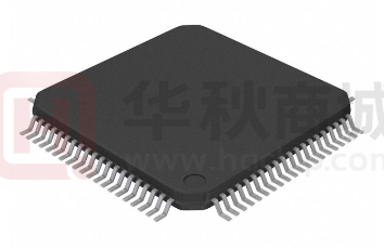


 工商网监
湘ICP备2023018690号
工商网监
湘ICP备2023018690号
