To our customers,
Old Company Name in Catalogs and Other Documents
On April 1st, 2010, NEC Electronics Corporation merged with Renesas Technology
Corporation, and Renesas Electronics Corporation took over all the business of both
companies. Therefore, although the old company name remains in this document, it is a valid
Renesas Electronics document. We appreciate your understanding.
Renesas Electronics website: http://www.renesas.com
April 1st, 2010
Renesas Electronics Corporation
Issued by: Renesas Electronics Corporation (http://www.renesas.com)
Send any inquiries to http://www.renesas.com/inquiry.
�Notice
1.
2.
3.
4.
5.
6.
7.
All information included in this document is current as of the date this document is issued. Such information, however, is
subject to change without any prior notice. Before purchasing or using any Renesas Electronics products listed herein, please
confirm the latest product information with a Renesas Electronics sales office. Also, please pay regular and careful attention to
additional and different information to be disclosed by Renesas Electronics such as that disclosed through our website.
Renesas Electronics does not assume any liability for infringement of patents, copyrights, or other intellectual property rights
of third parties by or arising from the use of Renesas Electronics products or technical information described in this document.
No license, express, implied or otherwise, is granted hereby under any patents, copyrights or other intellectual property rights
of Renesas Electronics or others.
You should not alter, modify, copy, or otherwise misappropriate any Renesas Electronics product, whether in whole or in part.
Descriptions of circuits, software and other related information in this document are provided only to illustrate the operation of
semiconductor products and application examples. You are fully responsible for the incorporation of these circuits, software,
and information in the design of your equipment. Renesas Electronics assumes no responsibility for any losses incurred by
you or third parties arising from the use of these circuits, software, or information.
When exporting the products or technology described in this document, you should comply with the applicable export control
laws and regulations and follow the procedures required by such laws and regulations. You should not use Renesas
Electronics products or the technology described in this document for any purpose relating to military applications or use by
the military, including but not limited to the development of weapons of mass destruction. Renesas Electronics products and
technology may not be used for or incorporated into any products or systems whose manufacture, use, or sale is prohibited
under any applicable domestic or foreign laws or regulations.
Renesas Electronics has used reasonable care in preparing the information included in this document, but Renesas Electronics
does not warrant that such information is error free. Renesas Electronics assumes no liability whatsoever for any damages
incurred by you resulting from errors in or omissions from the information included herein.
Renesas Electronics products are classified according to the following three quality grades: “Standard”, “High Quality”, and
“Specific”. The recommended applications for each Renesas Electronics product depends on the product’s quality grade, as
indicated below. You must check the quality grade of each Renesas Electronics product before using it in a particular
application. You may not use any Renesas Electronics product for any application categorized as “Specific” without the prior
written consent of Renesas Electronics. Further, you may not use any Renesas Electronics product for any application for
which it is not intended without the prior written consent of Renesas Electronics. Renesas Electronics shall not be in any way
liable for any damages or losses incurred by you or third parties arising from the use of any Renesas Electronics product for an
application categorized as “Specific” or for which the product is not intended where you have failed to obtain the prior written
consent of Renesas Electronics. The quality grade of each Renesas Electronics product is “Standard” unless otherwise
expressly specified in a Renesas Electronics data sheets or data books, etc.
“Standard”:
8.
9.
10.
11.
12.
Computers; office equipment; communications equipment; test and measurement equipment; audio and visual
equipment; home electronic appliances; machine tools; personal electronic equipment; and industrial robots.
“High Quality”: Transportation equipment (automobiles, trains, ships, etc.); traffic control systems; anti-disaster systems; anticrime systems; safety equipment; and medical equipment not specifically designed for life support.
“Specific”:
Aircraft; aerospace equipment; submersible repeaters; nuclear reactor control systems; medical equipment or
systems for life support (e.g. artificial life support devices or systems), surgical implantations, or healthcare
intervention (e.g. excision, etc.), and any other applications or purposes that pose a direct threat to human life.
You should use the Renesas Electronics products described in this document within the range specified by Renesas Electronics,
especially with respect to the maximum rating, operating supply voltage range, movement power voltage range, heat radiation
characteristics, installation and other product characteristics. Renesas Electronics shall have no liability for malfunctions or
damages arising out of the use of Renesas Electronics products beyond such specified ranges.
Although Renesas Electronics endeavors to improve the quality and reliability of its products, semiconductor products have
specific characteristics such as the occurrence of failure at a certain rate and malfunctions under certain use conditions. Further,
Renesas Electronics products are not subject to radiation resistance design. Please be sure to implement safety measures to
guard them against the possibility of physical injury, and injury or damage caused by fire in the event of the failure of a
Renesas Electronics product, such as safety design for hardware and software including but not limited to redundancy, fire
control and malfunction prevention, appropriate treatment for aging degradation or any other appropriate measures. Because
the evaluation of microcomputer software alone is very difficult, please evaluate the safety of the final products or system
manufactured by you.
Please contact a Renesas Electronics sales office for details as to environmental matters such as the environmental
compatibility of each Renesas Electronics product. Please use Renesas Electronics products in compliance with all applicable
laws and regulations that regulate the inclusion or use of controlled substances, including without limitation, the EU RoHS
Directive. Renesas Electronics assumes no liability for damages or losses occurring as a result of your noncompliance with
applicable laws and regulations.
This document may not be reproduced or duplicated, in any form, in whole or in part, without prior written consent of Renesas
Electronics.
Please contact a Renesas Electronics sales office if you have any questions regarding the information contained in this
document or Renesas Electronics products, or if you have any other inquiries.
(Note 1) “Renesas Electronics” as used in this document means Renesas Electronics Corporation and also includes its majorityowned subsidiaries.
(Note 2) “Renesas Electronics product(s)” means any product developed or manufactured by or for Renesas Electronics.
�PRELIMINARY PRODUCT INFORMATION
MOS INTEGRATED CIRCUIT
µPD78F9221CS, 78F9222CS
8-BIT SINGLE-CHIP MICROCONTROLLER
The µ PD78F9221CS, 78F9222CS are 8-bit single-chip microcontrollers of the 78K0S series.
These microcontrollers feature Single-voltage Self-programming Flash memory and many peripherals.
Detailed function descriptions are provided in the following user's manuals. Be sure to read them before
designing.
78K0S/KA1+ User’s Manual:
U16898E
78K/0S Series User's Manual Instruction:
U11047E
FEATURES
{ Minimum instruction execution time selectable from high speed (0.2 µs) to low speed (3.2 µs) (with CPU clock of
10 MHz)
{ General-purpose registers: 8 bits × 8 registers
{ ROM and RAM capacities
Item
Program Memory (Flash Memory)
Memory (Internal High-Speed RAM)
Part number
µPD78F9221CS
2 KB
128 bytes
µPD78F9222CS
4 KB
256 bytes
{ On-chip power-on clear (POC) circuit and low voltage detector (LVI)
{ On-chip watchdog timer (operable on internal low-speed internal oscillator clock)
{ I/O ports: 17
{ Timer: 4 channels
• 16-bit timer/event counter:
1 channel
• 8-bit timer:
2 channels
• Watchdog timer:
1 channel
{ Serial interface: UART (LIN (Local Interconnect Network) bus supported) 1 channel
{ 10-bit resolution A/D converter: 4 channels
{ Supply voltage: VDD = 2.0 to 5.5 VNote
{ Operating temperature range: TA = −40 to +85°C
Note Use this product in a voltage range of 2.2 to 5.5 V because the detection voltage (VPOC) of the power-on
clear (POC) circuit is 2.1 V ±0.1 V.
The information contained in this document is being issued in advance of the production cycle for the
product. The parameters for the product may change before final production or NEC Electronics
Corporation, at its own discretion, may withdraw the product prior to its production.
Not all products and/or types are availabe in every country. Please check with an NEC Electronics
sales representative for availability and additional information.
Document No. U18680EJ1V0PM00 (1st edition)
Date Published June 2007 NS CP(K)
Printed in Japan
2007
�µPD78F9221CS, 78F9222CS
APPLICATIONS
Automotive electronics, household appliances, toys, and industrial equipment
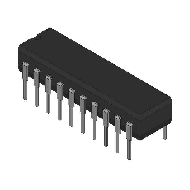
ORDERING INFORMATION
Part Number
µPD78F9221CS-CAC-A
µPD78F9222CS-CAC-A
Remark
2
Package
20-pin plastic SDIP (7.62 mm (300))
20-pin plastic SDIP (7.62 mm (300))
Products with -A at the end of the part number are lead-free products.
Preliminary Product Information U18680EJ1V0PM00
�µ PD78F9221CS, 78F9222CS
OVERVIEW OF FUNCTIONS
µPD78F9221CS
Item
Internal
memory
µPD78F9222CS
Flash memory
2 KB
4 KB
High-speed RAM
128 bytes
256 bytes
Memory space
64 KB
X1 input clock (oscillation frequency)
Crystal/ceramic/external clock input:
10 MHz (VDD = 2.0 to 5.5 V)
Internal
High speed (oscillation
oscillation
frequency)
clock
Low speed (for TMH1
Internal oscillation: 8 MHz (TYP.)
Internal oscillation: 240 kHz (TYP.)
and WDT)
General-purpose registers
8 bits × 8 registers
Instruction execution time
0.2 µs/0.4 µs/0.8 µs/1.6 µs/3.2 µs (X1 input clock: fX = 10 MHz)
I/O port
Total:
Timer
Timer output
17 pins
CMOS I/O:
15 pins
CMOS input:
1 pin
CMOS output:
1 pin
• 16-bit timer/event counter:
1 channel
• 8-bit timer (timer H1):
1 channel
• 8-bit timer (timer 80):
1 channel
• Watchdog timer:
1 channel
2 pins (PWM: 1 pin)
A/D converter
10-bit resolution × 4 channels
Serial interface
LIN-bus-supporting UART mode: 1 channel
Vectored
interrupt sources
External
4
Internal
9
• Reset by RESET pin
• Internal reset by watchdog timer
• Internal reset by power-on clear
Reset
• Internal reset by low-voltage detector
Note
Supply voltage
VDD = 2.0 to 5.5 V
Operating temperature range
TA = −40 to +85°C
Package
20-pin plastic SDIP
Note Use this product in a voltage range of 2.2 to 5.5 V because the detection voltage (VPOC) of the power-on- clear
(POC) circuit is 2.1 V ±0.1 V.
Preliminary Product Information U18680EJ1V0PM00
3
�µPD78F9221CS, 78F9222CS
PIN CONFIGURATION (Top View)
• 20-pin plastic SDIP
P23/ANI3
1
20
P130
P22/ANI2
2
19
P45
P21/ANI1
3
18
P44/RxD6
P20/ANI0
4
17
P43/TxD6/INTP1
AVREF
5
16
P42/TOH1
VSS
6
15
P41/INTP3
P121/X1
7
14
P40
P122/X2
8
13
P30/TI000/INTP0
P123
9
12
P31/TI010/TO00/INTP2
10
11
RESET/P34
VDD
Note In the µ PD78F9221CS, 78F9222CS, VSS functions alternately as the ground potential of the A/D converter.
Be sure to connect VSS to a stabilized GND (= 0 V).
ANI0 to ANI3:
4
Analog input
RESET:
Reset
AVREF:
Analog reference voltage
RxD6:
Receive data
INTP0 to INTP3:
External interrupt input
TI000, TI010:
Timer input
P20 to P23:
Port 2
TO00, TOH1:
Timer output
P30, P31, P34:
Port 3
TxD6:
Transmit data
P40 to P45:
Port 4
VDD:
Power supply
P121 to P123:
Port 12
VSS:
Ground
P130:
Port 13
X1, X2:
Crystal oscillator (X1 input clock)
Preliminary Product Information U18680EJ1V0PM00
�µ PD78F9221CS, 78F9222CS
BLOCK DIAGRAM
TO00/TI010/P31
Port 2
16-bit timer/event
counter 00
TI000/P30
Port 3
4
P20 to P23
2
P30, P31
P34
8-bit timer 80
TOH1/P42
8-bit timer H1
Low-speed
internal oscillator
78K0S
CPU
core
Flash
memory
Port 4
6
P40 to P45
Port 12
3
P121 to P123
Port 13
P130
Power on clear/
low voltage
indicator
POC/LVI
control
Watchdog timer
RxD6/P44
Serial interface
UART6
TxD6/P43
ANI0/P20 to
ANI3/P23
Internal
high-speed
RAM
4
Reset control
A/D converter
AVREF
RESET/P34
INTP0/P30
INTP1/P43
System control
Interrupt control
X1/P121
X2/P122
INTP2/P31
High-speed
internal oscillator
INTP3/P41
VDD
VSSNote
Note In the µ PD78F9221CS, 78F9222CS, VSS functions alternately as the ground potential of the A/D converter.
Be sure to connect VSS to a stabilized GND (= 0 V).
Preliminary Product Information U18680EJ1V0PM00
5
�µPD78F9221CS, 78F9222CS
CONTENTS
1.
PIN FUNCTIONS .................................................................................................................................. 7
1.1 Port Functions............................................................................................................................................. 7
1.2 Non-port Functions ..................................................................................................................................... 8
1.3 Pin I/O Circuits and Connection of Unused Pins ..................................................................................... 9
2.
ELECTRICAL SPECIFICATIONS (TARGET) ................................................................................... 11
3.
PACKAGE DRAWING ....................................................................................................................... 23
APPENDIX A. RELATED DOCUMENTS ................................................................................................. 24
6
Preliminary Product Information U18680EJ1V0PM00
�µ PD78F9221CS, 78F9222CS
1. PIN FUNCTIONS
1.1
Port Functions
Pin Name
I/O
Function
After Reset
AlternateFunction Pin
P20 to P23
I/O
Port 2.
Input
ANI0 to ANI3
Input
TI000/INTP0
4-bit I/O port.
Can be set to input or output mode in 1-bit units.
An on-chip pull-up resistor can be connected by setting software.
P30
I/O
Can be set to input or output mode in 1-
Port 3
bit units.
P31
TI010/TO00/
An on-chip pull-up resistor can be
INTP2
connected by setting software.
P34
Input
P40
I/O
Input only
Port 4.
Input
−
Input
6-bit I/O port.
P41
RESET
INTP3
Can be set to input or output mode in 1-bit units.
P42
TOH1
An on-chip pull-up resistor can be connected by setting software.
P43
TxD6/INTP1
P44
RxD6
−
P45
P121
I/O
Port 12.
Input
3-bit I/O port.
P122
X2
Can be set to input or output mode in 1-bit units.
P123
X1
−
An on-chip pull-up resistor can be connected only to P123 by
setting software.
P130
Output
Port 13.
Output
−
1-bit output-only port
Caution The P121/X1 and P122/X2 pins are pulled down during reset.
Preliminary Product Information U18680EJ1V0PM00
7
�µPD78F9221CS, 78F9222CS
1.2
Non-port Functions
Pin Name
I/O
Function
After Reset
AlternateFunction Pin
INTP0
Input
External interrupt input for which the valid edge (rising edge,
Input
falling edge, or both rising and falling edges) can be specified
INTP1
P30/TI000
P43/TxD6
INTP2
P31/TI010/TO00
INTP3
P41
RxD6
Input
Serial data input for asynchronous serial interface
Input
P44
TxD6
Output
Serial data output for asynchronous serial interface
Input
P43/INTP1
TI000
Input
External count clock input to 16-bit timer/event counter 00.
Input
P30/INTP0
Capture trigger input to capture registers (CR000 and CR010) of
16-bit timer/event counter 00
TI010
Capture trigger input to capture register (CR000) of 16-bit
P31/TO00/INTP2
timer/event counter 00
TO00
Output
16-bit timer/event counter 00 output
Input
P31/TI010/INTP2
TOH1
Output
8-bit timer H1 output
Input
P42
ANI0 to ANI3
Input
Analog input of A/D converter
Input
P20 to P23
AVREF
−
Reference voltage of A/D converter
−
−
RESET
Input
System reset input
−
P34
X1
Input
Connection of crystal/ceramic resonator for system clock
−
P121
−
P122
oscillation.
External clock input
X2
−
Connection of crystal/ceramic resonator for system clock
oscillation.
VDD
−
Positive power supply
−
−
VSS
−
Ground potential
−
−
Caution The P121/X1 and P122/X2 pins are pulled down during reset.
8
Preliminary Product Information U18680EJ1V0PM00
�µ PD78F9221CS, 78F9222CS
1.3
Pin I/O Circuits and Connection of Unused Pins
Table 1-1 shows I/O circuit type of each pin and the connections of unused pins.
For the configuration of the I/O circuit of each type, refer to Figure 1-1.
Table 1-1. Types of Pin I/O Circuits and Connection of Unused Pins
Pin Name
P20/ANI0 to P23/ANI3
I/O Circuit Type
I/O
I/O
11
Recommended Connection of Unused Pin
Input:
Independently connect to AVREF or VSS via a resistor.
Output: Leave open.
P30/TI000/INTP0
8-A
Input:
Independently connect to VDD or VSS via a resistor.
Output: Leave open.
P31/TI010/TO00/INTP2
P34/RESET
2
Input
P40
8-A
I/O
Connect to VDD via a resistor.
Input:
Independently connect to VDD or VSS via a resistor.
Output: Leave open.
P41/INTP3
P42/TOH1
P43/TxD6/INTP1
P44/RxD6
P45
P121/X1
16-B
Input:
P122/X2
P123
Independently connect to VSS via a resistor.
Output: Leave open.
8-A
Input:
Independently connect to VDD or VSS via a resistor.
Output: Leave open.
P130
AVREF
3-C
−
Output
Leave open.
Input
Directly connect to VDD.
Preliminary Product Information U18680EJ1V0PM00
9
�µPD78F9221CS, 78F9222CS
Figure 1-1. Pin I/O Circuits
Type 2
VDD
Type 11
Pull up
enable
P-ch
AVREF
Data
P-ch
IN
IN/OUT
Output
disable
N-ch
VSS
Schmitt-triggered input with hysteresis characteristics
Comparator
P-ch
+
N-ch
VSS
AVREF
Input
enable
Type 3-C
Type 16-B
Feedback
cut-off
P-ch
VDD
P-ch
Data
OUT
X1,
IN/OUT
OSC
enable
X2,
IN/OUT
N-ch
VSS
VDD
Data
P-ch
Type 8-A
Output
disable
VDD
N-ch
VSS
Pull up
enable
P-ch
VDD
Data
Data
P-ch
P-ch
IN/OUT
Output
disable
N-ch
Output
Disable
VSS
10
Preliminary Product Information U18680EJ1V0PM00
N-ch
VSS
�µ PD78F9221CS, 78F9222CS
2. ELECTRICAL SPECIFICATIONS (TARGET)
These specifications are only target values, and may not be satisfied by mass-produced products.
Absolute Maximum Ratings (TA = 25°C)
Parameter
Supply voltage
Input voltage
Symbol
Conditions
Ratings
Unit
VDD
−0.3 to +6.5
V
VSS
−0.3 to +0.3
V
AVREF
−0.3 to VDD + 0.3
VI1
−0.3 to VDD + 0.3
VI2
Note
P30, P31, P34, P40 to P45, P121 to P123
P20 to P23
Note
−0.3 to AVREF + 0.3
Note
V
V
V
and −0.3 to VDD + 0.3
Note
Output voltage
VO
−0.3 to VDD + 0.3
Analog input voltage
VAN
−0.3 to AVREF + 0.3
Note
Note
V
V
and −0.3 to VDD + 0.3
Note
Output current, high
Output current, low
Operating ambient
IOH
IOL
−10.0
mA
Total of pins other than P20 to P23
−44.0
mA
Total of P20 to P23
−44.0
mA
Per pin
20.0
mA
Total of all pins
44.0
mA
−40 to +85
°C
TA
In normal operation mode
Tstg
Flash memory blank status
−65 to +150
°C
Flash memory programming already performed
−40 to +125
°C
temperature
Storage temperature
Per pin
During flash memory programming
Note Must be 6.5 V or lower
Caution Product quality may suffer if the absolute maximum rating is exceeded even momentarily for any
parameter. That is, the absolute maximum ratings are rated values at which the product is on the
verge of suffering physical damage, and therefore the product must be used under conditions that
ensure that the absolute maximum ratings are not exceeded.
Remark
Unless specified otherwise, the characteristics of alternate-function pins are the same as those of port pins.
Preliminary Product Information U18680EJ1V0PM00
11
�µPD78F9221CS, 78F9222CS
X1 Oscillator Characteristics (TA = −40 to +85°C, VDD = 2.0 to 5.5 VNote 1, VSS = 0 V)
Resonator
Ceramic
Recommended Circuit
VSS X1
X2
VSS X1
Unit
2.0
10.0
MHz
X2
2.0
10.0
MHz
2.7 V ≤ VDD ≤ 5.5 V
2.0
10.0
MHz
2.0 V ≤ VDD < 2.7 V
2.0
5.0
2.7 V ≤ VDD ≤ 5.5 V
0.045
0.25
2.0 V ≤ VDD < 2.7 V
0.09
0.25
Oscillation
Note 2
frequency (fX)
C1
C2
X1
X1 input
Note 2
frequency (fX)
X1 input high/low-level width
(tXH, tXL)
Notes 1.
TYP.
C2
resonator
clock
MAX.
Oscillation
MIN.
frequency (fX)
C1
External
Conditions
Note 2
resonator
Crystal
Parameter
µs
Use this product in a voltage range of 2.2 to 5.5 V because the detection voltage (VPOC) of the power-onclear (POC) circuit is 2.1 V ±0.1 V.
2.
Indicates only oscillator characteristics. Refer to AC Characteristics for instruction execution time.
Caution When using the X1 oscillator, wire as follows in the area enclosed by the broken lines in the above
figures to avoid an adverse effect from wiring capacitance.
• Keep the wiring length as short as possible.
• Do not cross the wiring with the other signal lines.
• Do not route the wiring near a signal line through which a high fluctuating current flows.
• Always make the ground point of the oscillator capacitor the same potential as VSS.
• Do not ground the capacitor to a ground pattern through which a high current flows.
• Do not fetch signals from the oscillator.
Remark
For the resonator selection and oscillator constant, users are required to either evaluate the oscillation
themselves or apply to the resonator manufacturer for evaluation.
12
Preliminary Product Information U18680EJ1V0PM00
�µ PD78F9221CS, 78F9222CS
High-Speed Internal Oscillator Characteristics (TA = −40 to +85°C, VDD = 2.0 to 5.5 VNote 1, VSS = 0 V)
Resonator
Parameter
Conditions
High-speed internal
Oscillation frequency (fX = 8
oscillator
MHz
) deviation
Note 2
Oscillation frequency (fX)
Notes 1.
2.7 V ≤ VDD ≤ 5.5 V
Note 2
MAX.
Unit
TA = −10 to +80°C
±3
%
TA = −40 to +85°C
±5
%
2.0 V ≤ VDD < 2.7 V
MIN.
TYP.
5.5
MHz
Use this product in a voltage range of 2.2 to 5.5 V because the detection voltage (VPOC) of the power-onclear (POC) circuit is 2.1 V ±0.1 V.
2.
Indicates only oscillator characteristics. Refer to AC Characteristics for instruction execution time.
Low-Speed Internal Oscillator Characteristics (TA = −40 to +85°C, VDD = 2.0 to 5.5 VNote, VSS = 0 V)
Resonator
Low-speed internal
Parameter
Conditions
Oscillation frequency (fRL)
MIN.
TYP.
MAX.
Unit
120
240
480
kHz
oscillator
Note Use this product in a voltage range of 2.2 to 5.5 V because the detection voltage (VPOC) of the power-on-clear
(POC) circuit is 2.1 V ±0.1 V.
Preliminary Product Information U18680EJ1V0PM00
13
�µPD78F9221CS, 78F9222CS
DC Characteristics (TA = −40 to +85°C, VDD = 2.0 to 5.5 VNote, VSS = 0 V) (1/2)
Parameter
Output current, high
Symbol
IOH1
IOH2
Output current, low
Input voltage, high
Input voltage, low
Output voltage, high
IOL
Conditions
MIN.
TYP.
MAX.
Unit
Pins other than
Per pin
2.0 V ≤ VDD ≤ 5.5 V
–5
mA
P20 to P23
Total
4.0 V ≤ VDD ≤ 5.5 V
–25
mA
2.0 V ≤ VDD < 4.0 V
–15
mA
Per pin
2.0 V ≤ AVREF ≤ 5.5 V
–5
mA
Total
2.0 V ≤ AVREF ≤ 5.5 V
–15
mA
Per pin
2.0 V ≤ VDD ≤ 5.5 V
10
mA
Total of all pins
4.0 V ≤ VDD ≤ 5.5 V
30
mA
2.0 V ≤ VDD < 4.0 V
15
mA
0.8VDD
VDD
V
P20 to P23
VIH1
P30, P31, P34, P40 to P45, P123
VIH2
P20 to P23
0.7AVREF
AVREF
V
VIH3
P121, P122
0.8VDD
VDD
V
VIL1
P30, P31, P34, P40 to P45, P123
0
0.2VDD
V
VIL2
P20 to P23
0
0.3AVREF
V
VIL3
P121, P122
0
0.2VDD
V
VOH1
Total of pins other than
4.0 V ≤ VDD ≤ 5.5 V
P20 to P23
IOH1 = –5 mA
VDD − 1.0
V
VDD – 0.5
V
IOH1 = –15 mA
VOH2
IOH1 = –100 µA
2.0 V ≤ VDD < 4.0 V
Total of pins P20 to P23
4.0 V ≤ AVREF ≤ 5.5 V AVREF – 1.0
IOH2 = –10 mA
IOH2 = –5 mA
2.0 V ≤ AVREF < 4.0 V
V
AVREF – 0.5
V
IOH2 = –100 µA
Output voltage, low
VOL
Total of pins
4.0 V ≤ VDD ≤ 5.5 V
IOL = 30 mA
IOL = 10 mA
2.0 V ≤ VDD ≤ 4.0 V
1.3
V
0.4
V
IOL = 400 µA
Input leakage current, high ILIH1
VI = VDD
Pins other than X1
1
µA
Input leakage current, low
VI = 0 V
Pins other than X1
–1
µA
Output leakage current, high ILOH
VO = VDD
Pins other than X2
1
µA
Output leakage current, low
ILOL
VO = 0 V
Pins other than X2
–1
µA
Pull-up resistance
RPU
VI = 0 V
10
30
100
kΩ
Pull-down resistance
RPD
P121, P122, reset status
10
30
100
kΩ
ILIL1
Note Use this product in a voltage range of 2.2 to 5.5 V because the detection voltage (VPOC) of the power-on-clear
(POC) circuit is 2.1 V ±0.1 V.
Remark
14
Unless specified otherwise, the characteristics of alternate-function pins are the same as those of port pins.
Preliminary Product Information U18680EJ1V0PM00
�µ PD78F9221CS, 78F9222CS
DC Characteristics (TA = −40 to +85°C, VDD = 2.0 to 5.5 VNote 1, VSS = 0 V) (2/2)
Parameter
Symbol
Note 3
Supply
IDD1
Note 2
current
Conditions
Crystal/ceramic
fX = 10 MHz
oscillation, external
VDD = 5.0 V ±10%
fX = 6 MHz
clock input
oscillation operating
mode
Note 6
MIN. TYP. MAX. Unit
When A/D converter is stopped
6.1
12.2
When A/D converter is operating
7.6
15.2
When A/D converter is stopped
5.5
11.0
Note 4
Note 8
VDD = 5.0 V ±10%
When A/D converter is operating
fX = 5 MHz
When A/D converter is stopped
Note 4
Note 8
IDD2
3.0
6.0
When A/D converter is operating
4.5
9.0
Crystal/ceramic
fX = 10 MHz
When peripheral functions are stopped
1.7
3.8
oscillation, external
VDD = 5.0 V ±10%
When peripheral functions are operating
fX = 6 MHz
When peripheral functions are stopped
clock input HALT
mode
Note 6
Note 8
mA
14.0
VDD = 3.0 V ±10%
Note 5
mA
mA
mA
Note 4
VDD = 5.0 V ±10%
When peripheral functions are operating
fX = 5 MHz
When peripheral functions are stopped
6.7
1.3
3.0
mA
Note 4
VDD = 3.0 V ±10%
When peripheral functions are operating
High-speed internal
fX = 8 MHz
When A/D converter is stopped
oscillation operating
VDD = 5.0 V ±10%
High-speed internal
fX = 8 MHz
oscillation HALT
VDD = 5.0 V ±10%
When peripheral functions are operating
VDD = 5.0 V ±10%
When low-speed internal oscillation
6.0
0.48
1
mA
Note 5
Note 3
IDD3
5.0
10.0
When A/D converter is operating
6.5
13.0
When peripheral functions are stopped
1.4
3.2
Note 4
Note 7
2.1
Note 8
mA
mode
IDD4
mA
Note 4
Note 7
5.9
mode
IDD5
STOP mode
3.5
20.0
17.5
32.0
3.5
15.5
11.0
26.0
µA
is stopped
When low-speed internal oscillation
is operating
VDD = 3.0 V ±10%
When low-speed internal oscillation
µA
is stopped
When low-speed internal oscillation
is operating
Notes 1.
Use this product in a voltage range of 2.2 to 5.5 V because the detection voltage (VPOC) of the power-onclear (POC) circuit is 2.1 V ±0.1 V.
2.
Total current flowing through the internal power supply (VDD). Peripheral operation current is included
(however, the current that flows through the pull-up resistors of ports is not included).
3.
These currents include peripheral operation currents.
4.
When the processor clock control register (PCC) is set to 00H.
5.
When the processor clock control register (PCC) is set to 02H.
6.
When crystal/ceramic oscillation clock, external clock input is selected as the system clock source using
the option byte.
7.
When the high-speed internal oscillation clock is selected as the system clock source using the option
byte.
8.
The current that flows through the AVREF pin is included.
Preliminary Product Information U18680EJ1V0PM00
15
�µPD78F9221CS, 78F9222CS
AC Characteristics
(1) Basic operation (TA = −40 to +85°C, VDD = 2.0 to 5.5 VNote 1, VSS = 0 V)
Parameter
Symbol
Cycle time (minimum
TCY
instruction execution time)
Conditions
MIN.
low-level width
tTIH,
4.0 V ≤ VDD ≤ 5.5 V
0.2
16
µs
3.0 V ≤ VDD < 4.0 V
0.33
16
µs
2.7 V ≤ VDD < 3.0 V
0.4
16
µs
2.0 V ≤ VDD < 2.7 V
1
16
µs
High-speed internal
4.0 V ≤ VDD ≤ 5.5 V
0.23
4.22
µs
oscillation clock
2.7 V ≤ VDD < 4.0 V
0.47
4.22
µs
0.95
4.22
µs
4.0 V ≤ VDD ≤ 5.5 V
2/fsam+
0.1
2.0 V ≤ VDD < 4.0 V
tINTH,
tINTL
RESET input low-level
tRSL
µs
Note 2
2/fsam+
0.2
width, low-level width
Unit
clock, external clock input
tTIL
Interrupt input high-level
MAX.
Crystal/ceramic oscillation
2.0 V ≤ VDD < 2.7 V
TI000 input high-level width,
TYP.
µs
Note 2
1
µs
2
µs
width
Notes 1.
Use this product in a voltage range of 2.2 to 5.5 V because the detection voltage (VPOC) of the power-onclear (POC) circuit is 2.1 V ±0.1 V.
2.
Selection of fsam = fXP, fXP/4, or fXP/256 is possible using bits 0 and 1 (PRM000, PRM001) of prescaler
mode register 00 (PRM00). Note that when selecting the TI000 valid edge as the count clock, fsam = fXP.
CPU Clock Frequency, Peripheral Clock Frequency
Parameter
Conditions
CPU Clock (fCPU)
Ceramic resonator,
4.0 V ≤ VDD ≤ 5.5 V
125 kHz ≤ fCPU ≤ 10 MHz
crystal resonator,
3.0 V ≤ VDD < 4.0 V
125 kHz ≤ fCPU ≤ 6 MHz
external clock
2.7 V ≤ VDD < 3.0 V
2.0 V ≤ VDD < 2.7 V
High-speed internal
4.0 V ≤ VDD ≤ 5.5 V
oscillator
2.7 V ≤ VDD < 4.0 V
2.0 V ≤ VDD < 2.7 V
Peripheral Clock (fXP)
500 kHz ≤ fXP ≤ 10 MHz
125 kHz ≤ fCPU ≤ 5 MHz
Note
125 kHz ≤ fCPU ≤ 2 MHz
500 kHz ≤ fXP ≤ 5 MHz
500 kHz (Typ.) ≤ fCPU ≤ 8 MHz (Typ.)
2 MHz (Typ.) ≤ fXP ≤ 8 MHz (Typ.)
500 kHz (Typ.) ≤ fCPU ≤ 4 MHz (Typ.)
Note
500 kHz (Typ.) ≤ fCPU ≤ 2 MHz (Typ.)
2 M Hz (Typ.) ≤ fXP ≤ 4 MHz (Typ.)
Note Use this product in a voltage range of 2.2 to 5.5 V because the detection voltage (VPOC) of the power-on-clear
(POC) circuit is 2.1 V ±0.1 V.
16
Preliminary Product Information U18680EJ1V0PM00
�µ PD78F9221CS, 78F9222CS
TCY vs. VDD (Crystal/Ceramic Oscillation Clock, External Clock Input)
60
16
Cycle time TCY [µs]
10
Guaranteed
operation range
1.0
0.4
0.33
0.1
1
2
3
4
5
6
5.5
2.7
Supply voltage VDD [V]
TCY vs. VDD (High-Speed Internal Oscillation Clock)
60
Cycle time TCY [µs]
10
4.22
Guaranteed
operation range
1.0
0.95
0.47
0.23
0.1
1
2
3
4
5
6
2.7
5.5
Supply voltage VDD [V]
Preliminary Product Information U18680EJ1V0PM00
17
�µPD78F9221CS, 78F9222CS
(2) Serial interface (TA = −40 to +85°C, VDD = 2.0 to 5.5 VNote, VSS = 0 V)
UART mode (UART6, dedicated baud rate generator output)
Parameter
Symbol
Conditions
MIN.
Transfer rate
TYP.
MAX.
Unit
312.5
kbps
Note Use this product in a voltage range of 2.2 to 5.5 V because the detection voltage (VPOC) of the power-on-clear
(POC) circuit is 2.1 V ±0.1 V.
AC Timing Test Points (Excluding X1 Input)
0.8VDD
0.8VDD
Test points
0.2VDD
0.2VDD
Clock Timing
1/fX
tXL
tXH
X1 input
TI000 Timing
tTIL
tTIH
TI000
Interrupt Input Timing
tINTL
tINTH
INTP0 to INTP3
RESET Input Timing
tRSL
RESET
18
Preliminary Product Information U18680EJ1V0PM00
�µ PD78F9221CS, 78F9222CS
A/D Converter Characteristics (TA = −40 to +85°C, 2.7 V ≤ AVREF ≤ VDD ≤ 5.5 V, VSS = 0 VNote 1)
Parameter
Symbol
Conditions
Resolution
Notes 2, 3
Overall error
AINL
Conversion time
tCONV
MIN.
TYP.
MAX.
Unit
10
10
10
bit
±0.2
±0.4
%FSR
±0.3
4.0 V ≤ AVREF ≤ 5.5 V
±0.6
%FSR
4.5 V ≤ AVREF ≤ 5.5 V
3.0
100
µs
4.0 V ≤ AVREF < 4.5 V
4.8
100
µs
2.85 V ≤ AVREF < 4.0 V
6.0
100
µs
2.7 V ≤ AVREF < 2.85 V
14.0
2.7 V ≤ AVREF < 4.0 V
Notes 2, 3
Zero-scale error
Notes 2, 3
Full-scale error
Integral non-linearity error
100
µs
4.0 V ≤ AVREF ≤ 5.5 V
±0.4
%FSR
2.7 V ≤ AVREF < 4.0 V
±0.6
%FSR
Efs
4.0 V ≤ AVREF ≤ 5.5 V
±0.4
%FSR
2.7 V ≤ AVREF < 4.0 V
±0.6
%FSR
ILE
4.0 V ≤ AVREF ≤ 5.5 V
±2.5
LSB
2.7 V ≤ AVREF < 4.0 V
±4.5
LSB
4.0 V ≤ AVREF ≤ 5.5 V
±1.5
LSB
±2.0
LSB
AVREF
V
Ezs
Note 2
Note 2
Differential non-linearity error
DLE
Analog input voltage
VAIN
2.7 V ≤ AVREF < 4.0 V
Notes 1.
Note 1
VSS
In the 78K0S/KA1+, VSS functions alternately as the ground potential of the A/D converter. Be sure to
connect VSS to a stabilized GND (= 0 V).
2.
Excludes quantization error (±1/2 LSB).
3.
This value is indicated as a ratio (%FSR) to the full-scale value.
Caution The conversion accuracy may be degraded when the analog input pin is used as an alternate I/O
port or if a port is changed during A/D conversion.
Preliminary Product Information U18680EJ1V0PM00
19
�µPD78F9221CS, 78F9222CS
POC Circuit Characteristics (TA = −40 to +85°C)
Parameter
Symbol
Conditions
VPOC
Detection voltage
MIN.
TYP.
MAX.
Unit
2.0
2.1
2.2
V
µs
tPTH
VDD: 0 V → 2.1 V
Note 1
tPTHD
When power supply rises, after reaching
detection voltage (MAX.)
3.0
ms
Response delay time 2
Note 2
tPD
When power supply falls
1.0
ms
Minimum pulse width
tPW
Power supply boot time
Response delay time 1
Notes 1.
2.
1.5
0.2
ms
Time required from voltage detection to internal reset release.
Time required from voltage detection to internal reset signal generation.
POC Circuit Timing
Supply voltage
(VDD)
Detection voltage (MAX.)
Detection voltage (TYP.)
Detection voltage (MIN.)
tPW
tPTH
tPTHD
tPD
Time
20
Preliminary Product Information U18680EJ1V0PM00
�µ PD78F9221CS, 78F9222CS
LVI Circuit Characteristics (TA = −40 to +85°C)
Parameter
Symbol
Detection voltage
Note 1
MIN.
TYP.
MAX.
Unit
VLVI0
4.1
4.3
4.5
V
VLVI1
3.9
4.1
4.3
V
VLVI2
3.7
3.9
4.1
V
VLVI3
3.5
3.7
3.9
V
VLVI4
3.3
3.5
3.7
V
VLVI5
3.15
3.3
3.45
V
VLVI6
2.95
3.1
3.25
V
VLVI7
2.7
2.85
3.0
V
VLVI8
2.5
2.6
2.7
V
VLVI9
2.25
2.35
2.45
V
0.2
2.0
Response time
tLD
Minimum pulse width
tLW
Operation stabilization wait time
Notes 1.
2.
Note 2
Conditions
0.2
tLWAIT
ms
ms
0.1
0.2
ms
Time required from voltage detection to interrupt output or internal reset signal generation.
Time required from setting LVION to 1 to operation stabilization.
Remarks 1. VLVI0 > VLVI1 > VLVI2 > VLVI3 > VLVI4 > VLVI5 > VLVI6 > VLVI7 > VLVI8 > VLVI9
2. VPOC < VLVIm (m = 0 to 9)
LVI Circuit Timing
Supply voltage
(VDD)
Detection voltage (MAX.)
Detection voltage (TYP.)
Detection voltage (MIN.)
tLW
tLWAIT
LVION
tLD
1
Time
Data Memory STOP Mode Low Supply Voltage Data Retention Characteristics (TA = −40 to +85°C)
Parameter
Symbol
Conditions
MIN.
Data retention supply voltage
VDDDR
2.0
Release signal set time
tSREL
0
Preliminary Product Information U18680EJ1V0PM00
TYP.
MAX.
5.5
Unit
V
µs
21
�µPD78F9221CS, 78F9222CS
Flash Memory Programming Characteristics (TA = –40 to +85°C, 2.7 V ≤ VDD ≤ 5.5 V, VSS = 0 V)
Parameter
Supply current
Note 1
Erasure count
Symbol
Conditions
MIN.
TYP.
MAX.
Unit
7.0
mA
IDD
VDD = 5.5 V
NERASE
TA = −40 to +85°C
TCERASE
TA = −10 to +85°C,
4.5 V ≤ VDD ≤ 5.5 V
0.8
s
NERASE ≤ 100
3.5 V ≤ VDD < 4.5 V
1.0
s
2.7 V ≤ VDD < 3.5 V
1.2
s
TA = −10 to +85°C,
4.5 V ≤ VDD ≤ 5.5 V
4.8
s
NERASE ≤ 1000
3.5 V ≤ VDD < 4.5 V
5.2
s
2.7 V ≤ VDD < 3.5 V
6.1
s
TA = −40 to +85°C,
4.5 V ≤ VDD ≤ 5.5 V
1.6
s
NERASE ≤ 100
3.5 V ≤ VDD < 4.5 V
1.8
s
2.7 V ≤ VDD < 3.5 V
2.0
s
TA = −40 to +85°C,
4.5 V ≤ VDD ≤ 5.5 V
9.1
s
NERASE ≤ 1000
3.5 V ≤ VDD < 4.5 V
10.1
s
2.7 V ≤ VDD < 3.5 V
12.3
s
TA = −10 to +85°C,
4.5 V ≤ VDD ≤ 5.5 V
0.4
s
NERASE ≤ 100
3.5 V ≤ VDD < 4.5 V
0.5
s
2.7 V ≤ VDD < 3.5 V
0.6
s
TA = −10 to +85°C,
4.5 V ≤ VDD ≤ 5.5 V
2.6
s
NERASE ≤ 1000
3.5 V ≤ VDD < 4.5 V
2.8
s
2.7 V ≤ VDD < 3.5 V
3.3
s
1000
Times
(per 1 block)
Chip erase time
Block erase time
TBERASE
TA = −40 to +85°C,
4.5 V ≤ VDD ≤ 5.5 V
0.9
s
NERASE ≤ 100
3.5 V ≤ VDD < 4.5 V
1.0
s
2.7 V ≤ VDD < 3.5 V
1.1
s
TA = −40 to +85°C,
4.5 V ≤ VDD ≤ 5.5 V
4.9
s
NERASE ≤ 1000
3.5 V ≤ VDD < 4.5 V
5.4
s
2.7 V ≤ VDD < 3.5 V
6.6
s
Byte write time
TWRITE
TA = −40 to +85°C, NERASE ≤ 1000
150
µs
Internal verify
TVERIFY
Per 1 block
6.8
ms
Per 1 byte
27
µs
Blank check
TBLKCHK
Per 1 block
480
µs
Retention years
, NERASE ≤ 1000
Note 2
TA = 85°C
10
Years
Notes 1. Depending on the erasure count (NERASE), the erase time varies. Refer to the chip erase time and block
erase time parameters.
2. When the average temperature when operating and not operating is 85°C.
Remark When a product is first written after shipment, “erase → write” and “write only” are both taken as one rewrite.
22
Preliminary Product Information U18680EJ1V0PM00
�µ PD78F9221CS, 78F9222CS
3. PACKAGE DRAWING
20-PIN PLASTIC SDIP (7.62mm (300))
D
11
20
E
10
1
B
A
e1
A2
C
L
A1
b2
b1
Z
b
e
x
M
θ
c
C A B
A
(UNIT:mm)
ITEM
DIMENSIONS
D
17.57 MAX.
E
6.60
A
A1
A2
e
3.70 MAX.
0.65 ± 0.10
2.80
1.778
e1
7.62
b
0.52 ± 0.10
b1
1.02 ± 0.10
b2
0.77 ± 0.10
c
0.27 ± 0.07
L
2.86 ± 0.20
x
0.25
θ
Z
0° to 5°
0.609
P20CS-70-CAC
NEC Electronics Corporation 2007
Preliminary Product Information U18680EJ1V0PM00
23
�µPD78F9221CS, 78F9222CS
APPENDIX A. RELATED DOCUMENTS
The related documents indicated in this publication may include preliminary versions.
However, preliminary
versions are not marked as such.
Documents Related to Devices
Document Name
Document No.
µPD78F9221CS, 78F9222CS Preliminary Product Information
This manual
78K0S/KA1+ User’s Manual
U16898E
78K/0S Series Instructions User’s Manual
U11047E
Documents Related to Development Software Tools (User’s Manuals)
Document Name
RA78K0S Assembler Package
Document No.
Operation
U16656E
Language
U14877E
Structured Assembly Language
U11623E
Operation
U16654E
Language
U14872E
ID78K0S-NS Ver. 2.52 Integrated Debugger
Operation
U16584E
ID78K0S-QB Ver. 2.81 Integrated Debugger
Operation
U17287E
CC78K0S C Compiler
PM plus Ver. 5.20
U16934E
Documents Related to Development Hardware Tools (User’s Manuals)
Document Name
Document No.
IE-78K0S-NS In-Circuit Emulator
U13549E
IE-78K0S-NS-A In-Circuit Emulator
U15207E
QB-78K0SKX1MINI In-Circuit Emulator
U17272E
QB-78K0SKX1 In-Circuit Emulator
U18219E
QB-MINI2 On-Chip Debug Emulator with Programming Function
U18371E
Documents Related to Flash Memory Writing (User’s Manuals)
Document Name
Document No.
PG-FP4 Flash Memory Programmer
U15260E
PG-FPL2 Flash Memory Programmer
U17307E
Caution
The related documents listed above are subject to change without notice. Be sure to use the latest
version of each document for designing.
24
Preliminary Product Information U18680EJ1V0PM00
�µ PD78F9221CS, 78F9222CS
Other Related Documents
Document Name
Document No.
SEMICONDUCTOR SELECTION GUIDE - Products and Packages -
X13769X
Semiconductor Device Mount Manual
Note
Quality Grades on NEC Semiconductor Devices
C11531E
NEC Semiconductor Device Reliability/Quality Control System
C10983E
Guide to Prevent Damage for Semiconductor Devices by Electrostatic Discharge (ESD)
C11892E
Note See the “Semiconductor Device Mount Manual” website (http://www.necel.com/pkg/en/mount/index.html).
Caution
The related documents listed above are subject to change without notice. Be sure to use the latest
version of each document for designing.
Preliminary Product Information U18680EJ1V0PM00
25
�µPD78F9221CS, 78F9222CS
NOTES FOR CMOS DEVICES
1
VOLTAGE APPLICATION WAVEFORM AT INPUT PIN
Waveform distortion due to input noise or a reflected wave may cause malfunction. If the input of the
CMOS device stays in the area between VIL (MAX) and VIH (MIN) due to noise, etc., the device may
malfunction. Take care to prevent chattering noise from entering the device when the input level is fixed,
and also in the transition period when the input level passes through the area between VIL (MAX) and
VIH (MIN).
2
HANDLING OF UNUSED INPUT PINS
Unconnected CMOS device inputs can be cause of malfunction. If an input pin is unconnected, it is
possible that an internal input level may be generated due to noise, etc., causing malfunction. CMOS
devices behave differently than Bipolar or NMOS devices. Input levels of CMOS devices must be fixed
high or low by using pull-up or pull-down circuitry. Each unused pin should be connected to VDD or GND
via a resistor if there is a possibility that it will be an output pin. All handling related to unused pins must
be judged separately for each device and according to related specifications governing the device.
3
PRECAUTION AGAINST ESD
A strong electric field, when exposed to a MOS device, can cause destruction of the gate oxide and
ultimately degrade the device operation. Steps must be taken to stop generation of static electricity as
much as possible, and quickly dissipate it when it has occurred.
Environmental control must be
adequate. When it is dry, a humidifier should be used. It is recommended to avoid using insulators that
easily build up static electricity. Semiconductor devices must be stored and transported in an anti-static
container, static shielding bag or conductive material. All test and measurement tools including work
benches and floors should be grounded.
The operator should be grounded using a wrist strap.
Semiconductor devices must not be touched with bare hands. Similar precautions need to be taken for
PW boards with mounted semiconductor devices.
4
STATUS BEFORE INITIALIZATION
Power-on does not necessarily define the initial status of a MOS device. Immediately after the power
source is turned ON, devices with reset functions have not yet been initialized. Hence, power-on does
not guarantee output pin levels, I/O settings or contents of registers. A device is not initialized until the
reset signal is received. A reset operation must be executed immediately after power-on for devices
with reset functions.
5
POWER ON/OFF SEQUENCE
In the case of a device that uses different power supplies for the internal operation and external
interface, as a rule, switch on the external power supply after switching on the internal power supply.
When switching the power supply off, as a rule, switch off the external power supply and then the
internal power supply. Use of the reverse power on/off sequences may result in the application of an
overvoltage to the internal elements of the device, causing malfunction and degradation of internal
elements due to the passage of an abnormal current.
The correct power on/off sequence must be judged separately for each device and according to related
specifications governing the device.
6
INPUT OF SIGNAL DURING POWER OFF STATE
Do not input signals or an I/O pull-up power supply while the device is not powered. The current
injection that results from input of such a signal or I/O pull-up power supply may cause malfunction and
the abnormal current that passes in the device at this time may cause degradation of internal elements.
Input of signals during the power off state must be judged separately for each device and according to
related specifications governing the device.
26
Preliminary Product Information U18680EJ1V0PM00
�µ PD78F9221CS, 78F9222CS
SuperFlash is a registered trademark of Silicon Storage Technology, Inc. in several countries including the
United States and Japan.
Caution: This product uses SuperFlash® technology licensed from Silicon Storage Technology, inc.
• The information contained in this document is being issued in advance of the production cycle for the
product. The parameters for the product may change before final production or NEC Electronics
Corporation, at its own discretion, may withdraw the product prior to its production.
• Not all products and/or types are available in every country. Please check with an NEC Electronics sales
representative for availability and additional information.
• No part of this document may be copied or reproduced in any form or by any means without the prior written consent
of NEC Electronics. NEC Electronics assumes no responsibility for any errors that may appear in this document.
• NEC Electronics does not assume any liability for infringement of patents, copyrights or other intellectual property
rights of third parties by or arising from the use of NEC Electronics products listed in this document or any other
liability arising from the use of such products. No license, express, implied or otherwise, is granted under any
patents, copyrights or other intellectual property rights of NEC Electronics or others.
• Descriptions of circuits, software and other related information in this document are provided for illustrative purposes
in semiconductor product operation and application examples. The incorporation of these circuits, software and
information in the design of a customer's equipment shall be done under the full responsibility of the customer. NEC
Electronics assumes no responsibility for any losses incurred by customers or third parties arising from the use of
these circuits, software and information.
• While NEC Electronics endeavors to enhance the quality, reliability and safety of NEC Electronics products,
customers agree and acknowledge that the possibility of defects thereof cannot be eliminated entirely. To minimize
risks of damage to property or injury (including death) to persons arising from defects in NEC Electronics products,
customers must incorporate sufficient safety measures in their design, such as redundancy, fire-containment and
anti-failure features.
• NEC Electronics products are classified into the following three quality grades: "Standard", "Special" and "Specific".
The "Specific" quality grade applies only to NEC Electronics products developed based on a customer-designated
"quality assurance program" for a specific application. The recommended applications of an NEC Electronics
products depend on its quality grade, as indicated below. Customers must check the quality grade of each NEC
Electronics product before using it in a particular application.
"Standard": Computers, office equipment, communications equipment, test and measurement equipment, audio and
visual equipment, home electronic appliances, machine tools, personal electronic equipment and
industrial robots.
"Special": Transportation equipment (automobiles, trains, ships, etc.), traffic control systems, anti-disaster
systems, anti-crime systems, safety equipment and medical equipment (not specifically designed for life
support).
"Specific": Aircraft, aerospace equipment, submersible repeaters, nuclear reactor control systems, life support
systems and medical equipment for life support, etc.
The quality grade of NEC Electronics products is "Standard" unless otherwise expressly specified in NEC
Electronics data sheets or data books, etc. If customers wish to use NEC Electronics products in applications
not intended by NEC Electronics, they must contact an NEC Electronics sales representative in advance to
determine NEC Electronics' willingness to support a given application.
(Note)
(1) "NEC Electronics" as used in this statement means NEC Electronics Corporation and also includes its
majority-owned subsidiaries.
(2) "NEC Electronics products" means any product developed or manufactured by or for NEC Electronics (as
defined above).
M5D 02. 11-1
Preliminary Product Information U18680EJ1V0PM00
27
�µPD78F9221CS, 78F9222CS
For further information,
please contact:
NEC Electronics Corporation
1753, Shimonumabe, Nakahara-ku,
Kawasaki, Kanagawa 211-8668,
Japan
Tel: 044-435-5111
http://www.necel.com/
[America]
[Europe]
[Asia & Oceania]
NEC Electronics America, Inc.
2880 Scott Blvd.
Santa Clara, CA 95050-2554, U.S.A.
Tel: 408-588-6000
800-366-9782
http://www.am.necel.com/
NEC Electronics (Europe) GmbH
Arcadiastrasse 10
40472 Düsseldorf, Germany
Tel: 0211-65030
http://www.eu.necel.com/
NEC Electronics (China) Co., Ltd
7th Floor, Quantum Plaza, No. 27 ZhiChunLu Haidian
District, Beijing 100083, P.R.China
Tel: 010-8235-1155
http://www.cn.necel.com/
Hanover Office
Podbielskistrasse 166 B
30177 Hannover
Tel: 0 511 33 40 2-0
Munich Office
Werner-Eckert-Strasse 9
81829 München
Tel: 0 89 92 10 03-0
Stuttgart Office
Industriestrasse 3
70565 Stuttgart
Tel: 0 711 99 01 0-0
United Kingdom Branch
Cygnus House, Sunrise Parkway
Linford Wood, Milton Keynes
MK14 6NP, U.K.
Tel: 01908-691-133
Succursale Française
9, rue Paul Dautier, B.P. 52
78142 Velizy-Villacoublay Cédex
France
Tel: 01-3067-5800
Sucursal en España
Juan Esplandiu, 15
28007 Madrid, Spain
Tel: 091-504-2787
Tyskland Filial
Täby Centrum
Entrance S (7th floor)
18322 Täby, Sweden
Tel: 08 638 72 00
Filiale Italiana
Via Fabio Filzi, 25/A
20124 Milano, Italy
Tel: 02-667541
Shanghai Branch
Room 2509-2510, Bank of China Tower,
200 Yincheng Road Central,
Pudong New Area, Shanghai, P.R.China P.C:200120
Tel:021-5888-5400
http://www.cn.necel.com/
Shenzhen Branch
Unit 01, 39/F, Excellence Times Square Building,
No. 4068 Yi Tian Road, Futian District, Shenzhen,
P.R.China P.C:518048
Tel:0755-8282-9800
http://www.cn.necel.com/
NEC Electronics Hong Kong Ltd.
Unit 1601-1613, 16/F., Tower 2, Grand Century Place,
193 Prince Edward Road West, Mongkok, Kowloon, Hong Kong
Tel: 2886-9318
http://www.hk.necel.com/
NEC Electronics Taiwan Ltd.
7F, No. 363 Fu Shing North Road
Taipei, Taiwan, R. O. C.
Tel: 02-8175-9600
http://www.tw.necel.com/
NEC Electronics Singapore Pte. Ltd.
238A Thomson Road,
#12-08 Novena Square,
Singapore 307684
Tel: 6253-8311
http://www.sg.necel.com/
NEC Electronics Korea Ltd.
11F., Samik Lavied’or Bldg., 720-2,
Yeoksam-Dong, Kangnam-Ku,
Seoul, 135-080, Korea
Tel: 02-558-3737
http://www.kr.necel.com/
Branch The Netherlands
Steijgerweg 6
5616 HS Eindhoven
The Netherlands
Tel: 040 265 40 10
G0706
�


 工商网监
湘ICP备2023018690号
工商网监
湘ICP备2023018690号
