DATASHEET
X9221A
FN8163
Rev 2.00
August 30, 2006
64 Taps, 2-Wire Serial Bus Dual Digitally Controlled Potentiometer (XDCP™)
FEATURES
DESCRIPTION
• Two XDCPs in one package
• 2-wire serial interface
• Register oriented format, 8 registers total
—Directly write wiper position
—Read wiper position
—Store as many as four positions per pot
• Instruction format
—Quick transfer of register contents to resistor
array
• Direct write cell
—Endurance–100,000 writes per bit per register
• Resistor array values
—2k, 10k, 50k
• Resolution: 64 taps each pot
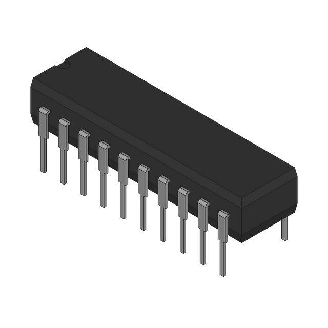
• 20 Ld plastic DIP and 20 Ld SOIC packages
• Pb-free plus anneal available (RoHS compliant)
The X9221A integrates two digitally controlled potentiometers (XDCP) on a monolithic CMOS integrated
microcircuit.
The digitally controlled potentiometer is implemented
using 63 resistive elements in a series array. Between
each element are tap points connected to the wiper
terminal through switches. The position of the wiper on
the array is controlled by the user through the 2-wire
bus interface. Each potentiometer has associated with
it a volatile Wiper Counter Register (WCR) and 2 nonvolatile Data Registers (DR0:DR1) that can be directly
written to and read by the user. The contents of the
WCR controls the position of the wiper on the resistor
array through the switches. Power up recalls the contents of DR0 to the WCR.
The XDCP can be used as a three-terminal potentiometer or as a two-terminal variable resistor in a wide
variety of applications including control, parameter
adjustments, and signal processing.
BLOCK DIAGRAM
Pot 0
VCC
VSS
R0 R1
R2 R3
SCL
SDA
A0
A1
A2
A3
Interface
and
Control
Circuitry
VL0/RL0
VW0/RW0
8
Data
R0 R1
R2 R3
FN8163 Rev 2.00
August 30, 2006
VH0/RH0
Wiper
Counter
Register
(WCR)
VH1/RH1
Wiper
Counter
Register
(WCR)
Register
Array
Pot 1
VL1/RL1
VW1/RW1
Page 1 of 15
�X9221A
Ordering Information
PART NUMBER
PART MARKING
VCC LIMITS
(V)
RTOTAL (k)
TEMP
RANGE (°C)
PKG.
DWG. #
5 ±10%
2
0 to +70
20 Ld SOIC (300MIL)
MDP0027
0 to +70
20 Ld SOIC (300MIL) (Pb-Free)
MDP0027
PACKAGE
X9221AYS
X9221AYS
X9221AYSZ (Note)
X9221AYS Z
X9221AYSI*
X9221AYSI
-40 to +85
20 Ld SOIC (300MIL)
MDP0027
X9221AYSIZ* (Note)
X9221AYSI Z
-40 to +85
20 Ld SOIC (300MIL) (Pb-Free)
MDP0027
X9221AWS*
X9221AWS
0 to +70
20 Ld SOIC (300MIL)
MDP0027
X9221AWSZ* (Note)
X9221AWS Z
0 to +70
20 Ld SOIC (300MIL) (Pb-Free)
MDP0027
X9221AWSI*
X9221AWSI
-40 to +85
20 Ld SOIC (300MIL)
MDP0027
X9221AWSIZ* (Note)
X9221AWSI Z
-40 to +85
20 Ld SOIC (300MIL) (Pb-Free)
MDP0027
X9221AUP
X9221AUP
0 to +70
20 Ld PDIP
MDP0031
X9221AUPZ (Note)
X9221AUPZ
0 to +70
20 Ld PDIP (Pb-Free)
MDP0031
X9221AUPI
X9221AUPI
-40 to +85
20 Ld PDIP
MDP0031
X9221AUPIZ (Note)
X9221AUPIZ
-40 to +85
20 Ld PDIP (Pb-Free)
MDP0031
X9221AUSI*
X9221AUSI
-40 to +85
20 Ld SOIC (300MIL)
MDP0027
X9221AUSIZ* (Note)
X9221AUSI Z
-40 to +85
20 Ld SOIC (300MIL) (Pb-Free)
MDP0027
10
50
*Add "T1" suffix for tape and reel.
NOTE: Intersil Pb-free plus anneal products employ special Pb-free material sets; molding compounds/die attach materials and
100% matte tin plate termination finish, which are RoHS compliant and compatible with both SnPb and Pb-free soldering operations.
Intersil Pb-free products are MSL classified at Pb-free peak reflow temperatures that meet or exceed the Pb-free requirements of
IPC/JEDEC J STD-020.
PIN DESCRIPTIONS
Potentiometer Pins
Host Interface Pins
VH/RH(VH0/RH0-VH1/RH1), VL/RL (VL0/RL0-VL1/RL1)
Serial Clock (SCL)
The VH/RH and VL/RL inputs are equivalent to the terminal connections on either end of a mechanical potentiometer.
The SCL input is used to clock data into and out of the
X9221A.
Serial Data (SDA)
SDA is a bidirectional pin used to transfer data into and
out of the device. It is an open drain output and may be
wire-ORed with any number of open drain or open collector outputs. An open drain output requires the use of
a pull-up resistor. For selecting typical values, refer to
the guidelines for calculating typical values on the bus
pull-up resistors graph.
Address
The Address inputs are used to set the least significant 4
bits of the 8-bit slave address. A match in the slave
address serial data stream must be made with the
Address input in order to initiate communication with the
X9221A
FN8163 Rev 2.00
August 30, 2006
VW/RW (VW0/RW0-VW1/RW1)
The wiper outputs are equivalent to the wiper output of a
mechanical potentiometer.
PIN CONFIGURATION
DIP/SOIC
VW0/RW0
1
20
VCC
VL0/RL0
2
19
RES
VH0/RL0
3
18
RES
A0
4
17
RES
A2
5
16
A1
VW1/RW1
6
15
A3
X9221A
VL1/RL1
7
14
SCL
VH1/RH1
8
13
RES
SDA
9
12
RES
VSS
10
11
RES
Page 2 of 15
�X9221A
Acknowledge
PIN NAMES
Symbol
Description
SCL
Serial Clock
SDA
Serial Data
A0–A3
Address
VH0/RH0-VH1/RH1,
VL0/RH0-VL1/RL0
Potentiometers
(terminal equivalent)
VW0/RW0-VW1/RW1
Potentiometers
(wiper equivalent)
RES
Reserved (Do not connect)
PRINCIPLES OF OPERATION
The X9221A is a highly integrated microcircuit incorporating two resistor arrays, their associated registers and
counters and the serial interface logic providing direct
communication between the host and the XDCP potentiometers.
Serial Interface
The X9221A supports a bidirectional bus oriented protocol. The protocol defines any device that sends data
onto the bus as a transmitter and the receiving device as
the receiver. The device controlling the transfer is a
master and the device being controlled is the slave. The
master will always initiate data transfers and provide the
clock for both transmit and receive operations. Therefore, the X9221A will be considered a slave device in all
applications.
Clock and Data Conventions
Data states on the SDA line can change only during SCL
LOW periods (tLOW). SDA state changes during SCL
HIGH are reserved for indicating start and stop conditions.
Start Condition
All commands to the X9221A are preceded by the start
condition, which is a HIGH to LOW transition of SDA
while SCL is HIGH (tHIGH). The X9221A continuously
monitors the SDA and SCL lines for the start condition,
and will not respond to any command until this condition
is met.
Acknowledge is a software convention used to provide a
positive handshake between the master and slave
devices on the bus to indicate the successful receipt of
data. The transmitting device, either the master or the
slave, will release the SDA bus after transmitting eight
bits. The master generates a ninth clock cycle and
during this period the receiver pulls the SDA line LOW to
acknowledge that it successfully received the eight bits
of data. See Figure 7.
The X9221A will respond with an acknowledge after recognition of a start condition and its slave address and
once again after successful receipt of the command
byte. If the command is followed by a data byte the
X9221A will respond with a final acknowledge.
Array Description
The X9221A is comprised of two resistor arrays. Each
array contains 63 discrete resistive segments that are
connected in series. The physical ends of each array are
equivalent to the fixed terminals of a mechanical potentiometer (VH/RH and VL/RL inputs).
At both ends of each array and between each resistor
segment is a FET switch connected to the wiper
(VW/RW) output. Within each individual array only one
switch may be turned on at a time. These switches are
controlled by the Wiper Counter Register (WCR). The
six least significant bits of the WCR are decoded to
select, and enable, one of sixty-four switches.
The WCR may be written directly, or it can be changed
by transferring the contents of one of four associated
data registers into the WCR. These data registers and
the WCR can be read and written by the host system.
Device Addressing
Following a start condition the master must output the
address of the slave it is accessing. The most significant
four bits of the slave address are the device type identifier (refer to Figure 1 below). For the X9221A this is fixed
as 0101[B].
Figure 1. Slave Address
Device Type
Identifier
Stop Condition
All communications must be terminated by a stop condition, which is a LOW to HIGH transition of SDA while
SCL is HIGH.
FN8163 Rev 2.00
August 30, 2006
0
1
0
1
A3
A2
A1
A0
Device Address
Page 3 of 15
�X9221A
The next four bits of the slave address are the device
address. The physical device address is defined by the
state of the A0-A3 inputs. The X9221A compares the
serial data stream with the address input state; a successful compare of all four address bits is required for
the X9221A to respond with an acknowledge.
Acknowledge Polling
The disabling of the inputs, during the internal nonvolatile write operation, can be used to take advantage of the
typical 5ms EEPROM write cycle time. Once the stop
condition is issued to indicate the end of the nonvolatile
write command the X9221A initiates the internal write
cycle. ACK polling can be initiated immediately. This
involves issuing the start condition followed by the
device slave address. If the X9221A is still busy with the
write operation no ACK will be returned. If the X9221A
has completed the write operation an ACK will be
returned and the master can then proceed with the next
operation.
Flow 1. ACK Polling Sequence
Nonvolatile Write
Command Completed
Enter ACK Polling
Issue
START
Issue Slave
Address
ACK
Returned?
Issue STOP
NO
YES
Further
Operation?
NO
YES
Issue
Instruction
Issue STOP
Proceed
Proceed
Instruction Structure
The next byte sent to the X9221A contains the instruction and register pointer information. The four most significant bits are the instruction. The next four bits point to
one of two pots and when applicable they point to one of
four associated registers. The format is shown below in
Figure 2.
Figure 2. Instruction Byte Format
t
Potentiometer
Select
I3
I2
I1
Instructions
I0
0
P0
R1
R0
Register
Select
The four high order bits define the instruction. The sixth
bit (P0) selects which one of the two potentiometers is to
be affected by the instruction. The last two bits (R1 and
R0) select one of the four registers that is to be acted
upon when a register oriented instruction is issued.
Four of the nine instructions end with the transmission of
the instruction byte. The basic sequence is illustrated in
Figure 3. These two-byte instructions exchange data
between the WCR and one of the data registers. A transfer from a data register to a WCR is essentially a write to
a static RAM. The response of the wiper to this action
will be delayed tSTPWV. A transfer from WCR’s current
wiper position to a data register is a write to nonvolatile
memory and takes a minimum of tWR to complete. The
transfer can occur between either potentiometer and
their associated registers or it may occur between both
of the potentiometers and one of their associated registers.
Four instructions require a three-byte sequence to complete. These instructions transfer data between the host
and the X9221A; either between the host and one of the
data registers or directly between the host and the WCR.
These instructions are: Read WCR, read the current
wiper position of the selected pot; Write WCR, change
current wiper position of the selected pot; Read Data
Register, read the contents of the selected nonvolatile
register; Write Data Register, write a new value to the
selected data register. The sequence of operations is
shown in Figure 4.
The Increment/Decrement command is different from
the other commands. Once the command is issued and
the X9221A has responded with an acknowledge, the
master can clock the selected wiper up and/or down in
one segment steps; thereby, providing a fine tuning
capability to the host. For each SCL clock pulse (tHIGH)
FN8163 Rev 2.00
August 30, 2006
Page 4 of 15
�X9221A
the VL/RL terminal. A detailed illustration of the
sequence and timing for this operation are shown in Figures 5 and 6 respectively.
while SDA is HIGH, the selected wiper will move one
resistor segment towards the VH/RH terminal. Similarly,
for each SCL clock pulse while SDA is LOW, the
selected wiper will move one resistor segment towards
Figure 3. Two-Byte Command Sequence
SCL
SDA
S
T
A
R
T
0
1
0
1
A3
A2
A1
A0
A
C
K
I3
I2
I1
I0
0
P0
0
0
R1 R0
A
C
K
S
T
O
P
Figure 4. Three-Byte Command Sequence
SCL
SDA
S
T
A
R
T
0
1
0
1 A3 A2 A1 A0 A
C
K
I3 I2
I1 I0
0
P0 R1 R0 A
C
K
D5 D4 D3 D2 D1 D0 A
C
K
S
T
O
P
Figure 5. Increment/Decrement Command Sequined
e
SCL
X
SDA
S
T
A
R
0
1
T
FN8163 Rev 2.00
August 30, 2006
0
1
A3 A2 A1 A0
A
C
K
I3
I2
I1
I0
0
X
P0 R1 R0 A
C
K
I
N
C
1
I
N
C
2
I
N
C
n
D
E
C
1
D
E
C
n
S
T
O
P
Page 5 of 15
�X9221A
Figure 6. Increment/Decrement Timing Limits
INC/DEC
CMD
Issued
tCLWV
SCL
SDA
Voltage Out
VW/RW
Table 1. Instruction Set
Instruction Format
Instruction
I3
I2
I1
I0
0
Read WCR
1
0
0
1
0
Write WCR
1
0
1
0
Read Data Register
1
0
1
Write Data Register
1
1
XFR Data Register to
WCR
1
XFR WCR to Data
Register
R0
Operation
1/0
N/A(7)
N/A
Read the contents of the Wiper Counter Register
pointed to by P0
0
1/0
N/A
N/A
Write new value to the Wiper Counter Register
pointed to by P0
1
0
1/0
1/0
1/0
Read the contents of the Register pointed to by
P0 and R1–R0
0
0
0
1/0
1/0
1/0
Write new value to the Register pointed to by P0
and R1–R0
1
0
1
0
1/0
1/0
1/0
Transfer the contents of the Register pointed to
by P0 and R1–R0 to its associated WCR
1
1
1
0
0
1/0
1/0
1/0
Transfer the contents of the WCR pointed to by
P0 to the Register pointed to by R1–R0
Global XFR Data
Register to WCR
0
0
0
1
N/A
N/A
1/0
1/0
Transfer the contents of the Data Registers
pointed to by R1–R0 of both pots to their
respective WCR
Global XFR WCR
to Data Register
1
0
0
0
N/A
N/A
1/0
1/0
Transfer the contents of all WCRs to their
respective data Registers pointed to by R1–R0
of both pots
Increment/Decrement
Wiper
0
0
1
0
0
1/0
N/A
N/A
Enable Increment/decrement of the WCR pointed to by P0
Note:
P0
R1
(7) N/A = Not applicable or don’t care; that is, a data register is not involved in the operation and need not be addressed (typical)
FN8163 Rev 2.00
August 30, 2006
Page 6 of 15
�X9221A
Figure 7. Acknowledge Response from Receiver
SCL from
Master
1
8
9
Data Output
from Transmitter
Data Output
from Receiver
START
DETAILED OPERATION
Both XDCP potentiometers share the serial interface
and share a common architecture. Each potentiometer
is comprised of a resistor array, a wiper counter register
and four data registers. A detailed discussion of the register organization and array operation follows.
Wiper Counter Register
The X9221A contains two wiper counter registers
(WCR), one for each XDCP potentiometer. The WCR
can be envisioned as a 6-bit parallel and serial load
counter with its outputs decoded to select one of sixtyfour switches along its resistor array. The contents of the
WCR can be altered in four ways: it may be written
directly by the host via the Write WCR instruction (serial
load); it may be written indirectly by transferring the contents of one of four associated data registers via the
XFR Data Register instruction (parallel load); it can be
modified one step at a time by the Increment/ Decrement instruction; finally, it is loaded with the contents of
its data register zero (R0) upon power-up.
FN8163 Rev 2.00
August 30, 2006
Acknowledge
The WCR is a volatile register; that is, its contents are
lost when the X9221A is powered-down. Although the
register is automatically loaded with the value in R0
upon power-up, it should be noted this may be different
from the value present at power-down.
Data Registers
Each potentiometer has four nonvolatile data registers.
These can be read or written directly by the host and
data can be transferred between any of the four data
registers and the WCR. It should be noted all operations
changing data in one of these registers is a nonvolatile
operation and will take a maximum of 10ms.
If the application does not require storage of multiple
settings for the potentiometer, these registers can be
used as regular memory locations that could possibly
store system parameters or user preference data.
Page 7 of 15
�X9221A
Figure 8. Detailed Potentiometer Block Diagram
Serial Data Path
Serial
Bus
Input
From Interface
Circuitry
Register 0
Register 1
8
Register 2
If WCR = 00[H] then VW/RW = VL/RL
If WCR = 3F[H] then VW/RW = VH/RH
VH/RH
6
Register 3
UP/DN
Modified SCL
Parallel
Bus
Input
Wiper
Counter
Register
INC/DEC
Logic
UP/DN
CLK
C
o
u
n
t
e
r
D
e
c
o
d
e
VL/RL
VW/RW
FN8163 Rev 2.00
August 30, 2006
Page 8 of 15
�X9221A
ABSOLUTE MAXIMUM RATINGS
COMMENT
Temperature Under Bias ................... -65°C to +135°C
Storage Temperature ........................ -65°C to +150°C
Voltage on SCK, SCL or Any Address
Input With Respect to VSS ...................... -1V to +7V
Voltage on Any VH/RH, VW/RW or VL/RL
Referenced to VSS ................................. +6V / -4.3V
V = |VH/RH–VL/RL|........................................... 10.3V
Lead Temperature (soldering, 10s) ................. +300°C
IW (10s) ..............................................................±6mA
Stresses above those listed under “Absolute Maximum
Ratings” may cause permanent damage to the device.
This is a stress rating only; functional operation of the
device (at these or any other conditions above those
indicated in the operational sections of this specification)
is not implied. Exposure to absolute maximum rating
conditions for extended periods may affect device reliability.
RECOMMENDED OPERATING CONDITIONS
Temp
Commercial
Industrial
Min.
0C
-40C
Max.
Supply Voltage
X9221A
+70C
+85C
Limits
5V ± 10%
ANALOG CHARACTERISTICS (Over recommended operating conditions unless otherwise stated.)
Limits
Symbol
RTOTAL
Parameter
End to End Resistance
Min.
Typ.
-20
Power Rating
IW
Wiper Current
RW
Wiper Resistance
VTERM
Voltage on any VH/RH, VW/RW or
VL/RL Pin
-3
40
-3.0
Noise
Resolution
Absolute Linearity(1)
Relative Linearity(2)
Temperature Coefficient
FN8163 Rev 2.00
August 30, 2006
Unit
+20
%
50
mW
+3
mA
130
+5
V
120
dBV
1.6
%
-1
-0.2
+1
MI(3)
+0.2
MI(3)
±300
Radiometric Temperature Coefficient
CH/CL/CW Potentiometer Capacitances
Max.
±20
10/10/25
Test Conditions
+25°C, each pot
Wiper Current = ±1mA
Ref: 1V
See Note 5
Vw(n)(actual - Vw(n)(expected)
Vw(n + 1) - [Vw(n) + MI]
ppm/°C
See Note 5
ppm/°C
See Note 5
pF
See circuit #3
Page 9 of 15
�X9221A
D.C. OPERATING CHARACTERISTICS (Over recommended operating conditions unless otherwise stated.)
Limits
Symbol
Parameter
lCC
Supply Current (Active)
ISB
VCC Current (Standby)
Min. Typ.
200
Max.
Unit
Test Conditions
3
mA
fSCL = 100kHz, SDA = Open, Other Inputs = VSS
500
µA
SCL = SDA = VCC, Addr. = VSS
ILI
Input Leakage Current
10
µA
VIN = VSS to VCC
ILO
Output Leakage Current
10
µA
VOUT = VSS to VCC
VIH
Input HIGH Voltage
2
VCC + 1
V
VIL
Input LOW Voltage
-1
0.8
V
VOL
Output LOW Voltage
0.4
V
IOL = 3mA
Notes: (1) Absolute Linearity is utilized to determine actual wiper voltage versus expected voltage as determined by wiper position when used as
a potentiometer.
(2) Relative Linearity is utilized to determine the actual change in voltage between two successive tap positions when used as a potentiometer. It is a measure of the error in step size.
(3) MI = RTOT/63 or (VH/RH–VL/RL)/63, single pot
ENDURANCE AND DATA RETENTION
Parameter
Min.
Unit
Minimum endurance
100,000
Data changes per bit per register
Data retention
100
years
CAPACITANCE
Symbol
(5)
(5)
CI/O
CIN
Parameter
Max.
Unit
Test Conditions
Input/output capacitance (SDA)
8
pF
VI/O = 0V
Input capacitance (A0, A1, A2, A3 and SCL)
6
pF
VIN = 0V
POWER-UP TIMING
Symbol
Parameter
Max.
Unit
Power-up to initiation of read operation
1
ms
Power-up to initiation of write operation
5
ms
50
V/ms
(6)
tPUW(6)
tRVCC
VCC Power-up ramp rate
tPUR
Min.
0.2
Notes: (5) This parameter is periodically sampled and not 100% tested.
(6) tPUR and tPUW are the delays required from the time VCC is stable until the specified operation can be initiated. These parameters are
periodically sampled and not 100% tested.
Power Up Requirements (Power up sequencing can affect correct recall of the wiper registers)
The preferred power-on sequence is as follows: First VCC, then the potentiometer pins. It is suggested that VCC
reach 90% of its final value before power is applied to the potentiometer pins. The VCC ramp rate specification should
be met, and any glitches or slope changes in the VCC line should be held to


 工商网监
湘ICP备2023018690号
工商网监
湘ICP备2023018690号
