RF2713
RF2713
Quadrature
Modulator/Demodulator
QUADRATURE MODULATOR/DEMODULATOR
RoHS Compliant & Pb-Free Product
Package Style: SOIC-14
I INPUT A 1
Features
3V to 6V Operation
Modulation or Demodulation
IF From 100kHz to 250MHz
Baseband From DC to 50MHz
Digital LO Quadrature Divider
Low Power and Small Size
I INPUT B 2
Q INPUT A 3
Q INPUT B 4
D
8 Q OUT
Functional Block Diagram
Product Description
The RF2713 is a monolithic integrated quadrature modulator/demodulator. The demodulator is used to recover the I and Q baseband signals from
the amplified and filtered IF. Likewise, the inputs and outputs can be
reconfigured to modulate I/Q signals onto an RF carrier. The RF2713 is
intended for IF systems where the IF frequency ranges from 100kHz to
250MHz, and the LO frequency is two times the IF. The IC contains all of
the required components to implement the modulation/demodulation
function and contains a digital divider type 90° phase shifter, two double
balanced mixers, and baseband amplifiers designed to interface with Analog to Digital Converters. The unit operates from a single 3V to 6V power
supply.
N
ot
Fo
Q IF OUT 7
ew
9 I OUT
rN
12 GND
10 GND
I IF OUT 6
Digital and Analog Receivers
and Transmitters
High Data Rate Digital Communications
Spread-Spectrum Communication Systems
Interactive Cable Systems
Portable Battery-Powered
Equipment
13 LO INPUT
11 GND
BG OUT 5
Applications
QUAD
DIV.
BY 2
es
ig
n
14 VCC
Ordering Information
RF2713
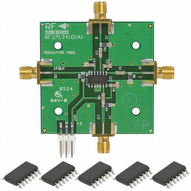
RF2713 PCBA-D
RF2713 PCBA-M
Quadrature Modulator/Demodulator
Fully Assembled Evaluation Board (Demodulator)
Fully Assembled Evaluation Board (Modulator)
Optimum Technology Matching® Applied
GaAs HBT
GaAs MESFET
InGaP HBT
SiGe BiCMOS
9Si BiCMOS
SiGe HBT
GaAs pHEMT
Si CMOS
Si BJT
GaN HEMT
RF MICRO DEVICES®, RFMD®, Optimum Technology Matching®, Enabling Wireless Connectivity™, PowerStar®, POLARIS™ TOTAL RADIO™ and UltimateBlue™ are trademarks of RFMD, LLC. BLUETOOTH is a trademark owned by Bluetooth SIG, Inc., U.S.A. and licensed for use by RFMD. All other trade names, trademarks and registered trademarks are the property of their respective owners. ©2006, RF Micro Devices, Inc.
Rev A7 DS130405
7628 Thorndike Road, Greensboro, NC 27409-9421 · For sales or technical
support, contact RFMD at (+1) 336-678-5570 or sales-support@rfmd.com.
1 of 16
�RF2713
Absolute Maximum Ratings
Parameter
Supply Voltage
IF Input Level
Rating
Unit
-0.5 to 7.0
VDC
500
mVPP
Operating Ambient Temperature
-40 to +85
°C
Storage Temperature
-40 to +150
°C
Caution! ESD sensitive device.
Exceeding any one or a combination of the Absolute Maximum Rating conditions may
cause permanent damage to the device. Extended application of Absolute Maximum
Rating conditions to the device may reduce device reliability. Specified typical performance or functional operation of the device under Absolute Maximum Rating conditions is not implied.
RoHS status based on EUDirective2002/95/EC (at time of this document revision).
Min.
Specification
Typ.
Max.
es
ig
n
Parameter
The information in this publication is believed to be accurate and reliable. However, no
responsibility is assumed by RF Micro Devices, Inc. ("RFMD") for its use, nor for any
infringement of patents, or other rights of third parties, resulting from its use. No
license is granted by implication or otherwise under any patent or patent rights of
RFMD. RFMD reserves the right to change component circuitry, recommended application circuitry and specifications at any time without prior notice.
Unit
T=25°C, VCC =3.0V, IF=100MHz,
LO=200MHz, FMOD =500kHz
IF Frequency Range
0.1
Baseband Frequency Range
DC
Level
rN
Frequency
0.06
Input Impedance
MHz
N
ot
:
Twice (2x) the IF frequency. For IF frequencies
below ~2.5MHz, the LO should be a square
wave. IF frequencies lower than 100kHz are
attainable if the LO is a square wave and sufficiently large DC blocking capacitors are used.
VPP
170 || 1pF
:
2.5
VPP
24
25.1
dB
VCC =3.0V
VCC =5.0V
dB
Single Sideband, IF Input of device reactively
matched
dB
Single Sideband, 50: shunt resistor at IF Input
24
Input Third Order Intercept Point
(IIP3)
-22
dBm
-11
dBm
33
Each output, IOUT and QOUT @ 1MHz
Saturated
dB
Noise Figure
28
Each input, single-ended
IFIN =28mVPP, LO=200mVPP, ZLOAD =10k:
20
22.5
For IF frequencies below ~2.5MHz, the LO
should be a square wave. IF frequencies lower
than 100kHz are attainable if the LO is a
square wave and sufficiently large DC blocking
capacitors are used.
:
Fo
Voltage Gain
0.8
500 || 1pF
Demodulator Configuration
Output Impedance
50
1200 || 1pF
LO
Maximum Output
MHz
ew
Input Impedance
265
D
Overall
VCC =3.0V, IF Input of device reactively
matched
VCC =3.0V, 50: shunt resistor at IF Input
VCC =5.0V, IF Input of device reactively
matched
-19
2 of 16
Condition
-8
dBm
VCC =5.0V, 50: shunt resistor at IF Input
-28
dBm
VCC =5.0V, IF Input of device reactively
matched, ZLOAD =50:
7628 Thorndike Road, Greensboro, NC 27409-9421 · For sales or technical
support, contact RFMD at (+1) 336-678-5570 or sales-support@rfmd.com.
Rev A7 DS130405
�RF2713
Parameter
Min.
Specification
Typ.
Max.
Unit
Demodulator Configuration,
cont.
Condition
IFIN =28mVPP, LO=200mVPP, ZLOAD =10k:
-21
-18.5
0.1
Quadrature Phase Error
DC Output
2.0
DC Offset
dBm
0.5
VCC =5.0V, 50: shunt at IF Input
dB
1
°
800
mV
VCC =3.0V, IOUT and QOUT to GND
VCC =5.0V, IOUT and QOUT to GND
2.4
2.8
V


 工商网监
湘ICP备2023018690号
工商网监
湘ICP备2023018690号
