ib technology
Data Sheet
UNI_RS232_USB.pdf
9 Pages
Last Revised 03/09/09
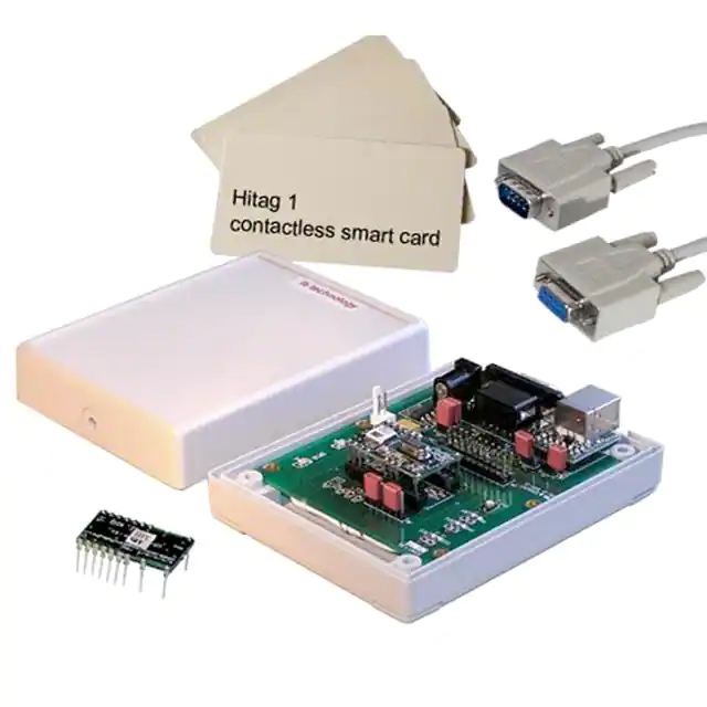
Universal RFID Socket board with RS232 / USB interface
The Universal RFID Socket board is the baseboard for the MicroRWD RFID reader modules
from IB Technology.
82 mm
75
mm
MicroRWD modules are low-cost, pin compatible and host command compatible Proximity
reader modules for Hitag 1, Hitag S256/2048, Hitag 2, Mifare 1k/4k/Ultralight, ICODE SLI
and EM400X/4102 RFID tags and contactless smart cards. The module solutions only require
a 5v supply and an antenna coil to be fully featured read/write systems with optimised easy to
use host commands. All modules use the same universal 24 pin DIP package so customers can
migrate between different transponder technology with the minimum of design change.
Mifare
Hitag 2
Quad Tag
ICODE
Hitag 1/S
EM Marin
The Universal Socket board provides the
antenna, power supply regulation and RS232 /
USB interfaces to the MicroRWD module
itself. Specifically the board has a 24 pin DIP
socket for the appropriate MicroRWD module
to be plugged into, LEDS for visual status
indication, selectable PCB and coil based
antenna for 13.56MHz and 125kHz operation
and voltage regulation allowing 9-12v DC
power supplies to be used.
The Universal Socket board with the
appropriate MicroRWD module fitted is a
complete “ready-to-use” RFID reader system
and is used in the SDK/Evaluation kit together
with sample tags/cards and CDROM containing
all the data sheets and Windows applications
(executable and C source).
1
�ib technology
Universal socket board (with 125kHz coil antenna mounted on the underside) was designed to
fit in the Evatron EVA73 plastic case giving the option of a fully enclosed product.
The Universal socket board can be powered directly from a stabilised 5 volt supply, from the
9-12 volt DC connector or from the USB bus. The MicroRWD module itself has a low
average current (approximately 15-20ma) but consumes up to 200ma in a short burst every
polling cycle when the RF is turned on for the brief communication period. The Universal
socket board uses a 470uF capacitor across the supply rails to smooth these current pulses and
so the entire board consumes around 60 ma and can operate directly from a USB bus with no
external power supply.
Universal socket board link options
The board has link options to select the on-board 13.56MHz PCB antenna or the external
125kHz antenna coil and various options for supplying power to the board and interfaces.
CON J6, 125kHz antenna connections
CON J8, 125kHz or 13.56MHz
antenna selection
AN3
AN1
AN5
AN4
CON J3, 0.1, 2-way pin
header, 5v stabilised supply
(GND, +5v)
RED GREEN LEDS
J7 connects power to
MAX202 RS232
converter
CON J1, 9-12v
DC, 2.5mm
Power Socket
(+ve centre pin)
RWD
Pin 1
AN2
AN6
RED LED
GRN LED
OP3
OP2
USB SLEEP
USB CLK
USB PWREN
USB RESET
0v GND
5v
J2 connects power from
regulator to board.
CON J10,
RS232 socket
(9-way female
D-type connector)
OP1
OP0
MCLR / (VPP)
RX / (DATA)
USB connector
TX / (CLK)
GND
CTS
SW1
0v GND
5v
CON J9, 2 x 10 x 0.1 inch pin header
J4 connects power to USB module
(all available signals, 5v supply and GND) J5 connects external USB bus 5v to board
1
2
�ib technology
Connector and link descriptions
a) CON J1 (2.5mm Power Socket (+ve centre pin):
Connector for external 9-12v DC supply.
b) Link J2 (2 pin, 0.1 inch header):
Connects 5 volt output from on-board voltage regulator to the rest of the board.
c) CON J3 (2 pin , 0.1 inch polarised connector):
Connector for external 5v stabilised power supply to board.
d) Link J4 (2 pin, 0.1 inch header):
Connects 5 volt supply on board to USB module.
e) Link J5 (2 pin, 0.1 inch header):
Connects external USB bus 5 volt supply to the rest of the board.
f) CON J6 (2 pin, 0.1 inch header):
Connection for external 125kHz, 700 uH antenna coil.
g) Link J7 (2 pin, 0.1 inch header):
Connects 5 volt supply on board to MAX202 RS232 level converter.
h) Links J8 (6 pin, 0.1 inch header):
Selects on-board 13.56MHz PCB antenna or external 125kHz antenna coil.
AN3
AN3
For 125 kHz antenna
link AN1-AN5
AN5
AN2-AN6
AN4
AN1
AN1
AN5
AN4
For 13.56 MHz antenna
link AN1-AN3
AN2-AN4
AN2
AN2
AN6
AN6
i) CON J9 (2 x 10 way, 0.1 inch header):
RED LED
GRN LED
OP3
OP2
USB SLEEP
USB CLK
USB PWREN
USB RESET
0v GND
5v
OP1
OP0
MCLR / (VPP)
RX / (DATA)
TX / (CLK)
GND
CTS
SW1
0v GND
5v
All available interface signals from
RWD module and USB module.
1
j) CON J10 (9 pin female, D-type):
RS232 connector (1, 4, 6 joined, 2 – Tx, 3 – Rx, 5 – GND, 8 – CTS)
3
�ib technology
Operation of MicroRWD module only with 5 volt external supply
With a MicroRWD module fitted and the 13.56MHz or 125kHz antenna selected, the module
can be powered from an external 5 volt stabilised supply connected to CON J3 or CON J9.
The interface and communication pins can also be accessed directly from CON J9. For this
case the links J2, J4, J5, J7 can be removed to ensure that only the MicroRWD module is
powered and the MAX202 and the USB module (if fitted) are OFF.
Operation of MicroRWD module using RS232 interface
The MicroRWD module can be powered from an external 5 volt stabilised or 9-12 volt unregulated supply (Link J2 set accordingly). For RS232 communication, link J7 should be
closed to power the MAX202 device. A standard RS232 extension cable (straight-through,
pin-to-pin) is used to connect CON J10 to a PC COM port or other host RS232 interface.
Operation of MicroRWD module using USB interface (if fitted)
The MicroRWD module can be connected to and powered from an external USB bus.
To ensure the board consumes minimum power, links J2 and J7 should be removed to
disconnect the MAX202 power and regulator supply. Links J4 and J5 should then be closed
to connect the external USB bus 5 volt supply to the USB module and the MicroRWD itself.
The Universal RFID socket board uses the low-cost FTDI (Future Technology Devices
International Ltd) MM232R “serial to USB converter” module. If not already fitted, the
module can be purchased on-line from http://www.ftdichip.com/
FTDI USB – serial interface module MM232R
The USB module should be connected to the PC USB port using a standard USB connecting
cable. All the Windows applications for the MicroRWD module currently communicate with
the serial COM ports and assume RS232 connection. FTDI provide a VCP (Virtual COM
Port) driver for the MM232R module that allows standard RS232 communication programs to
operate over the USB bus. The VCP drivers for various Operating Systems can be
downloaded from http://www.ftdichip.com/Drivers/VCP.htm and installed according to the
supplied instructions (VCP driver file: CDM 2.00.00 or later). With the Universal RFID
board connected to the USB bus, the Windows applications can be run in the usual manner
with a COM port selected higher than the maximum COM port number on the PC being used.
4
�ib technology
FTDI MM232R USB Module pin out and PCB pad layout
+5v
Link J4
2-way pin header
FTDI MM232R
USB/RS232 module, MOD1
C7
Rx
Connected to MicroRWD CTS,
Tx and Rx pins
Tx
CTS
USB SLEEP
USB CLK12
USB PWREN
USB RESET
0v GND
Link J5
2-way pin header
For USB powered RFID board, short linksJ4 and J5
For external 5v supply, short link J4, open link J5
5
�ib technology
RS232 interface circuit and connector pin out
(DCD, DTR, DSR joined)
MicroRWD CTS (BUSY) connected to CTS
+5v
1, 4, 6 - joined
2 – Tx
3 – Rx
5 – GND
8 - CTS
CON J7
2-way pin header
CTS
Tx
1
Rx
6
C15
Connected to MicroRWD CTS,
Tx and Rx pins
C14
+
C3
C17
C16
C18
1
16
2
15
MAX20214
3
U2
4
13
5
Rx 12
CTS 11
Tx 10
6
7
8
9
0v Ground Plane
6
9
5
CON J10, 9 way
D-Type socket
RS232 connector
�ib technology
MicroRWD module interface circuit and pin out
RWD +5v
D2
R1, R3 1k Red LED
24
1
CTS
Tx
D1, Green LED
MCLR/Vpp
Rx
RWD +5v
SW1
Micro
RWD
(MOD2)
OP3
R2, R8
OP2
0v GND
RWD +5v
AN3
AN1
AN5
AN4
OP0
R4, R9
OP1
CON J9, 2 x 10 x 0.1 inch
pin header
AN1
Red LED
Grn LED
OP3
OP2
USB SLEEP
USB CLK
USB PWREN
USB RESET
0v GND
5v
AN2
AN2
12
AN6
13
CON J8
For 125kHz antenna link AN1-AN5, AN2-AN6
For 13.56MHz ant’ link AN1-AN3, AN2, AN4
0v GND
C12 = 22pF
1 uH PCB antenna (L2)
C19, 5-50pF
trimming
capacitor
1
AN3
R6, 0R
C10 = 180pF
C11 = 220pF
AN4
R7, 0R
R5
C13 = 22pF
C8, C9
AN5
ANT1, L3
700uH Antenna
27R
47pF
AN6
47pF
Through hole solder pads for wire coil connection.
CON J3, 0.1, 2-way pin
header, 5v stabilised supply
RWD+5v
L1, 22uH
C2, 470uF
low ESR
+5v
47nF
C6
C5
C20
47nF
0v GND
C1
C4
CON J1, 9-12v DC, 2.5mm Power Jack
Socket (+ve centre pin)
Link J2
0.1, 2-way pin header
LM1117 REG (U1)
7
OP1
OP0
MCLR/Vpp
Rx(Data)
Tx(Clk)
GND
CTS
SW1
0v GND
5v
�ib technology
MicroRWD pin out
Pin Name
DIP No.
I/O Type
Buffer Type
LED1
LED2
RESET
1
2
3
O
O
I
TTL
TTL
ST
SW1
OP3
OP2
GND
VCC
AN1
AN2
GND
OP1
OP0
VCC
RX
TX
CTS
Description
Red LED connection. 25ma max sink current
Green LED connection. 25ma max sink current
Reset pin internally pulled high. Active low.
Normally not connected
4
I
ST
Switch input to override output drives or select baud
rate. Internally pulled high. Active low
5
O
TTL
Aux output drive. 25ma max sink current.
6
O
TTL
Aux output drive. 25ma max sink current.
7
P
Ground reference for logic and analogue pins
8
P
+5v Positive supply
9
P
AN
Antenna connection. Up to 200ma peak current. +/100v peak voltage. 125kHz or 13.56Mhz drive into
700 uH or 1 uH antenna.
10
Not connected
11
Not connected
12
P
AN
Antenna connection.
13
P
Ground reference for logic and analogue pins.
Normally used for antenna screen connection
14
Not connected
15
Not connected
16
Not connected
17
Not connected
18
Not connected
19
O
TTL
Aux output drive. 25ma max sink current.
20
O
TTL
Aux output drive. 25ma max sink current.
21
P
+5v Positive supply
22
I
TTL
Serial communication Receive line. 9600 baud, 8 bit,
1 stop, no parity
23
O
TTL
Serial communication Transmit line
24
O
TTL
Serial communication CTS handshake. RX enabled
when CTS low and disabled when high.
(I/O = Input/Output, AN = Antenna output, P = Power, ST = Schmitt Trigger input, TTL = TTL logic I/O)
Standard 0.1 inch / 2.54 mm
pitch. “wide” 24 pin DIL layout.
30.5 mm
24
1
Pins mounted to hybrid
flush with substrate.
Micro
RWD
PCB Row Spacing
17.5 mm
12
Unconnected pin pads
13
17.5mm
8
�ib technology
Universal RFID socket board specifications
Basic preliminary electrical specifications.
Parameter
Typical Value
Supply Voltage
Operating temperature
Average current consumption: MicroRWD + LEDs ONLY
(default 100ms RF-OFF polling delay)
Average current consumption: MicroRWD + LEDs +
RS232 interface.
Average current consumption: MicroRWD + LEDs + USB
interface.
Maximum board current (MicroRWD + all interfaces active)
Peak antenna voltage (optimum antenna tuning)
Peak antenna current (optimum tuning)
Communication time for Tag authentication
Communication time for 32 bit WRITE operation
Maximum data rate (between Tag and RWD)
Range (dependent on antenna dimensions and tuning)
Auxiliary output drive current
Switch input (pulled up)
Serial Interface
Communication Parameters (depending on MicroRWD type)
5v DC regulated or
9-12v DC unregulated.
-25 deg C to + 70 deg C
Approx 20ma
Approx 25ma
Approx 25ma
Approx 60ma
Up to +/- 100v (200v
peak-to-peak)
Up to 200ma
20ms (Hitag)
30ms (Hitag)
4k baud or 53 / 106k baud
Up to 20cm (125kHz) or
10cm (13.56MHz)
Up to 25ma sink
Active low
TTL level RS232 or +/12v RS232
9600/38400 baud, 8 data
bits, no parity, 1 stop bit
protocol with CTS
handshake
No responsibility is taken for the method of integration or final use of MicroRWD
More information on the Micro RWD and other products can be found at the Internet web site:
http://www.ibtechnology.co.uk
Or alternatively contact IB Technology by email at:
sales@ibtechnology.co.uk
9
�


 工商网监
湘ICP备2023018690号
工商网监
湘ICP备2023018690号
