®
RT8525D
Current Mode Boost Controller
General Description
Features
The RT8525D is a wide input operating voltage range step
up controller. High voltage output and large output current
are feasible by using an external N-MOSFET. The RT8525D
input operating range is from 4.5V to 25V.
The RT8525D is an optimized design for wide output voltage
range applications. The output voltage of the RT8525D can
be adjusted by the FB pin.
Ordering Information
Programmable Soft-Start Time
Programmable Boost SW Frequency from 50kHz to
600kHz
Output Over Voltage Protection
Output Under Voltage Protection
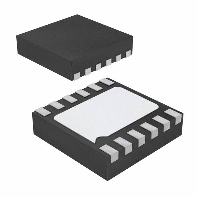
12-Lead WDFN Package
RoHS Compliant and Halogen Free
Applications
RT8525D
Package Type
QW : WDFN-12L 3x3 (W-Type)
(Exposed Pad-Option 2)
Lead Plating System
G : Green (Halogen Free and Pb Free)
Note :
LCD TV, Monitor Display Backlight
LED Driver Application
High Current High Output Voltage DC/DC Converters
High Input Voltage DC/DC Converters
Pin Configurations
(TOP VIEW)
RoHS compliant and compatible with the current require-
VDC
VIN
COMP
SS
FSW
FAULT
ments of IPC/JEDEC J-STD-020.
Suitable for use in SnPb or Pb-free soldering processes.
Marking Information
13
12
11
10
9
8
7
EN
DRV
GND
ISW
OVP
FB
WDFN-12L 3x3
0F= : Product Code
0F=YM
DNN
1
2
3
4
5
6
GND
Richtek products are :
VIN Range : 4.5V to 25V
YMDNN : Date Code
Simplified Application Circuit
L1
VIN
CIN
VDC
ISW
CDC
VOUT
M1
RSLP
RS
COMP
GND
CC2
RFB1
FSW
CC1
SS
RSW
CSS
Chip Enable
FB
FAULT
RFLT
ROVP1
12V
RFB2
OVP
EN
Copyright © 2014 Richtek Technology Corporation. All rights reserved.
DS8525D-01 August 2014
COUT
RT8525D
VIN
DRV
CVIN
RC
D1
COVP
ROVP2
is a registered trademark of Richtek Technology Corporation.
www.richtek.com
1
�RT8525D
Functional Pin Description
Pin No.
Pin Name
Pin Function
1
VDC
Output of Internal Pre-Regulator.
2
VIN
IC Power Supply.
3
COMP
Compensation for Error Amplifier. Connect a compensation network to ground.
4
SS
External Capacitor to Adjust Soft-Start Time.
5
FSW
Frequency Adjust Pin. This pin allows setting the switching frequency with a
resistor from 50kHz to 600kHz.
6
FAULT
Open Drain Output for Fault Detection.
7
FB
Feedback to Error Amplifier Input.
8
OVP
Sense Output Voltage for Over Voltage Protection and Under Voltage Protection.
9
ISW
External MOSFET Switch Current Sense Pin. Connect the current sense resistor
between the external N-MOSFET switch and ground.
10,
GND
13 (Exposed Pad)
Ground of Boost Controller. The exposed pad must be soldered to a large PCB
and connected to GND for maximum power dissipation.
11
DRV
Drive Output for the N-MOSFET.
12
EN
Chip Enable (Active High).
Copyright © 2014 Richtek Technology Corporation. All rights reserved.
www.richtek.com
2
is a registered trademark of Richtek Technology Corporation.
DS8525D-01 August 2014
�RT8525D
Function Block Diagram
FSW
VIN
VDC
UVLO
+
OTP
OVP/OUVP
Logic
12V LDO
FAULT
Protection
OSC
+
OC
-
EN
S
Q
R
Q
+
-
DRV
Blanking
+
-
PWM
Controller
2.5V
0.4V
VOS
GND
OVP
+
-
FAULT
0.1V
-
+
EA
-
4µA
ISW
1.25V
FB
COMP
SS
Operation
The RT8525D is a wide input operating voltage range and
current mode step up controller. High voltage output and
large output current are feasible by using an external NMOSFET.
The error amplifier EA adjusts COMP voltage by comparing
the feedback signal from the output voltage with the internal
1.25V reference.
Blanking
N-MOSFET current is measured by external RS. The slope
compensator works together with sensing voltage of
RSENSE to the ISW pin. There is need blanking time to
avoid noise and parasitism effect.
Fault Protection
The protection functions include output over voltage, output
under voltage, over temperature protection. The FAULT
pin will be pulled low once a protection is triggered, and a
suitable pulled-high RFLT is required. The detail description
can refer to the Figure 2. Fault Protection Function Block.
Copyright © 2014 Richtek Technology Corporation. All rights reserved.
DS8525D-01 August 2014
is a registered trademark of Richtek Technology Corporation.
www.richtek.com
3
�RT8525D
Absolute Maximum Ratings
(Note 1)
VIN to GND ------------------------------------------------------------------------------------------------------------------VDC, DRV, FAULT to GND -----------------------------------------------------------------------------------------------EN, COMP, SS, FSW, FB, OVP, ISW to GND ---------------------------------------------------------------------Power Dissipation, PD @ TA = 25°C
WDFN-12L 3x3 -------------------------------------------------------------------------------------------------------------Package Thermal Resistance (Note 2)
WDFN-12L 3x3, θJA -------------------------------------------------------------------------------------------------------WDFN-12L 3x3, θJC -------------------------------------------------------------------------------------------------------Lead Temperature (Soldering, 10 sec.) -------------------------------------------------------------------------------Junction Temperature -----------------------------------------------------------------------------------------------------Storage Temperature Range --------------------------------------------------------------------------------------------ESD Susceptibility (Note 3)
HBM (Human Body Model) ----------------------------------------------------------------------------------------------MM (Machine Model) ------------------------------------------------------------------------------------------------------
Recommended Operating Conditions
−0.3V to 26.4V
−0.3V to 13.2V
−0.3V to 6V
1.667W
60°C/W
8.2°C/W
260°C
150°C
−65°C to 150°C
2kV
200V
(Note 4)
Supply Input Voltage, VIN ------------------------------------------------------------------------------------------------ 4.5V to 25V
Junction Temperature Range --------------------------------------------------------------------------------------------- −40°C to 125°C
Ambient Temperature Range --------------------------------------------------------------------------------------------- −40°C to 85°C
Electrical Characteristics
(VIN = 21V, CIN = 10μF, TA = 25°C, unless otherwise specified)
Parameter
Symbol
Test Conditions
Min
Typ
Max Unit
Input Power Supply
Quiescent Current
IQ
No Switching, RSW = 56k
--
1.3
2
mA
Shutdown Current
Under Voltage Lockout
Threshold
Under Voltage Lockout
Hysteresis
12V Regulator
ISHDN
VEN = 0V
--
10
--
A
VUVLO
VIN Rising
--
3.8
--
V
--
500
--
mV
11.4
12
12.6
V
--
500
--
mV
--
270
--
mA
VUVLO
13.5V < VIN < 16V, 1mA < ILOAD < 100mA
Regulator Output Voltage
VDC
16V < VIN < 20V, 1mA < ILOAD < 50mA
20V < VIN < 25V, 1mA < ILOAD < 20mA
Dropout Voltage
VDROP
Short-Circuit Current Limit
ISC
VIN VDC, VIN = 12V, ILOAD = 100mA
VDC Short to GND
Control Input
EN Threshold Logic-High
Voltage
Logic-Low
VIH
2
--
--
VIL
--
--
0.8
EN Sink Current
IIH
--
5
--
VEN = 5V
Copyright © 2014 Richtek Technology Corporation. All rights reserved.
www.richtek.com
4
V
A
is a registered trademark of Richtek Technology Corporation.
DS8525D-01 August 2014
�RT8525D
Parameter
Shutdown
Delay
Symbol
Test Conditions
Min
Typ
Max
Unit
tSLEEP
RSW = 56k, EN = L, 12V Regular
Shutdown
55
--
--
ms
Shutdown Mode tSHDN
RSW = 56k, EN = L, IC Shutdown
110
--
--
ms
--
200
--
kHz
--
250
--
ns
90
--
--
%
Sleeping Mode
Boost Controller
Switching Frequency
fSW
RSW = 56k
Minimum On-Time
tMON
Maximum Duty
DMAX
Feedback Voltage
VFB
--
1.25
--
V
ISLOPE, PK
--
50
--
A
ISS
3
4
5
A
Switching
Slope Compensation
Peak Magnitude of Slope
Compensation Current
Soft-Start
Soft-Start Current
Gate Driver
RDS(ON)_N
ISINK = 100mA (N-MOSFET)
--
1
--
RDS(ON)_P
ISOURCE = 100mA (P-MOSFET)
--
1.5
--
Peak Sink Current
IPEAKsk
CLOAD = 1nF
--
2.2
--
A
Peak Source Current
IPEAKsr
CLOAD = 1nF
--
2.55
--
A
Rise Time
tr
CLOAD = 1nF
--
6
--
ns
Fall Time
tf
CLOAD = 1nF
--
5
--
ns
OCP Threshold
VOCP
Including Slope Compensation
Magnitude
--
0.4
--
V
VOUT OVP Threshold
VOVP
--
2.5
--
V
VOUT UVP Threshold
Thermal Shutdown
Temperature
Thermal Shutdown Hysteresis
VUVP
--
0.1
--
V
TSD
--
150
--
C
TSD
--
50
--
C
DRV On-Resistance
Protection Function
Note 1. Stresses beyond those listed “Absolute Maximum Ratings” may cause permanent damage to the device. These are
stress ratings only, and functional operation of the device at these or any other conditions beyond those indicated in
the operational sections of the specifications is not implied. Exposure to absolute maximum rating conditions may
affect device reliability.
Note 2. θJA is measured at TA = 25°C on a high effective thermal conductivity four-layer test board per JEDEC 51-7. θJC is
measured at the exposed pad of the package.
Note 3. Devices are ESD sensitive. Handling precaution is recommended.
Note 4. The device is not guaranteed to function outside its operating conditions..
Copyright © 2014 Richtek Technology Corporation. All rights reserved.
DS8525D-01 August 2014
is a registered trademark of Richtek Technology Corporation.
www.richtek.com
5
�RT8525D
Typical Application Circuit
VIN
5V
L1
10µH
CIN
22µF
2
CVIN
1µF
1
RT8525D
11
DRV
VIN
VDC
ISW
CDC
3 COMP
RC
5.6k
CC1
27nF
GND
CC2
RSW
56k
FAULT
12 EN
Copyright © 2014 Richtek Technology Corporation. All rights reserved.
www.richtek.com
6
9
M1
RSLP
2.4k
10,
13 (Exposed Pad)
OVP
RFLT
6 100k
VOUT
12V
COUT
22µF x 2
RS
50m
RFB1
43k
FB 7
5 FSW
4 SS
CSS
0.33µF
Chip Enable
D1
ROVP1
62k
12V
RFB2
3k
8
COVP
ROVP2
6k
is a registered trademark of Richtek Technology Corporation.
DS8525D-01 August 2014
�RT8525D
Typical Application Circuit
Quiescent Current vs. Temperature
3.0
2.5
2.5
Quiescent Current (mA)
Quiescent Current (mA)
Quiescent Current vs. Input Voltage
3.0
2.0
1.5
1.0
0.5
No Switching
9
14
19
24
1.5
1.0
0.5
No Switching
0.0
0.0
4
2.0
-50
29
-25
0
Feedback Voltage vs. Input Voltage
75
100
125
Feedback Voltage vs. Temperature
1.5
1.5
1.4
1.4
Feedback Voltage (V)
Feedback Voltage (V)
50
Temperature (°C)
Input Voltage (V)
1.3
1.2
1.1
1.0
1.3
1.2
1.1
1.0
4
9
14
19
24
29
-50
-25
0
25
50
75
100
125
Temperature (°C)
Input Voltage (V)
Boost Efficiency vs. Load Current
Switching Frequency vs. Temperature
300
100
260
90
Efficiency (%)
Switching Frequency (kHz)1
25
220
180
80
70
60
140
RSW = 56kΩ
VIN = 5V, VOUT = 12V, RSW = 56kΩ
50
100
-50
-25
0
25
50
75
100
Temperature (°C)
Copyright © 2014 Richtek Technology Corporation. All rights reserved.
DS8525D-01 August 2014
125
0
0.4
0.8
1.2
1.6
2
Load Current (A)
is a registered trademark of Richtek Technology Corporation.
www.richtek.com
7
�RT8525D
Applications Information
The RT8525D is a wide input operating voltage range step
up controller. High voltage output and large output current
are feasible by using an external N-MOSFET. The
protection functions include output over voltage, output
under voltage, over temperature and current limiting
protection.
Boost Output Voltage Setting
The regulated output voltage is set by an external resistor
divider according to the following equation :
R
VOUT = VFB 1+ FB1 , where VFB = 1.25V (typ.)
RFB2
The recommended value of RFB2 should be at least 1kΩ
for saving sacrificing. Moreover, placing the resistor divider
as close as possible to the chip can reduce noise
sensitivity.
Boost Switching Frequency
The RT8525D boost driver switching frequency is able to
be adjusted by a resistor RSW ranging from 18kΩ to
220kΩ. The following figure illustrates the corresponding
switching frequency within the resistor range.
Switching Frequency vs. RSW
600
f SW (kHz)
500
400
300
200
100
0
0
50
100
150
200
250
RSW (kΩ)
Figure 1. Boost Switching Frequency
Boost Loop Compensation
The voltage feedback loop can be compensated by an
external compensation network consisted of RC, CC1 and
CC2. Choose RC to set high frequency gain for fast
Copyright © 2014 Richtek Technology Corporation. All rights reserved.
www.richtek.com
8
transient response. Select CC1 and CC2 to set the zero
and pole to maintain loop stability. A typical compensation
for the RT8525D is choosing 3kΩ for RC and 27nF for CC1.
Soft-Start
The soft-start of the RT8525D can be achieved by
connecting a capacitor from the SS pin to GND. The builtin soft-start circuit reduces the start-up current spike and
output voltage overshoot. The external capacitor charged
by an internal 4μA constant charging current determines
the soft-start time. The SS pin limits the rising rate of the
COMP pin voltage and thereby limits the peak switch
current. The soft-start interval is set by the soft-start
capacitor according to the following equation :
tSS CSS 5 105
A typical value for the soft-start capacitor is 0.33μF. The
soft-start capacitor is discharged when EN voltage falls
below its threshold after shutdown delay or UVLO occurs.
Slope Compensation and Current Limiting
A slope compensation is applied to avoid sub-harmonic
oscillation in current-mode control. The slope
compensation voltage is generated by the internal ramp
current flow through a slope compensation resistor RSLP.
The inductor current is sensed by the sensing resistor
RS. Both of them are added and presented on the ISW
pin. The internal ramp current is rising linearly form zero
at the beginning of each switching cycle to 50μA in
maximum on-time of each cycle. The slope compensation
resistor RSLP can be calculated by the following equation :
VOUT VIN RS
RSLP >
2 L 50μ fSW
where RS is current sensing resistor, L is inductor value,
and fSW is boost switching frequency.
The current flow through inductor during charging period
is detected by a sensing resistor RS. Besides, the slope
compensation voltage also attributes magnitude to ISW.
As the voltage at the ISW pin is over 0.4V, the DRV will
be pulled low and turn off the external N-MOSFET. So
that the inductor will be forced to leave charging stage
and enter discharging stage to prevent over current. The
current limiting can be calculated by the following equation:
is a registered trademark of Richtek Technology Corporation.
DS8525D-01 August 2014
�RT8525D
0.4 DMAX RSLP 50μ
IL, PK
where IL, PK is peak inductor current, and DMAX is maximum
duty.
RS <
Output Over Voltage Protection
The output voltage can be clamped at the voltage level
determined by the following equation :
R
VOUT (OVP) = VOVP 1+ OVP1 ,
ROVP2
where VOVP = 2.5V (typ.)
where ROVP1 and ROVP2 are the voltage divider connected
to the OVP pin.
Fault Protection
The FAULT pin will be pulled low once a protection is
triggered, and a suitable pulled-high RFLT is required. The
suggested RFLT is 100kΩ if the pulled-high voltage was
12V. The following figure illustrates the fault protection
function block. If one of the OUVP and OTP occurs, the
switch 1 will be turned on, and the voltage at node A will
be under 0.25V. Then the protection function will perform
12V
action 2 to turn off the driver. When protection function is
released, the RT8525D will re-start.
On the other hand, if the triggered protection is OVP, the
voltage at node A will be decided by voltage divider
composed of RFLT and the internal 8kΩ resistor. This
voltage must be designed between 0.25V and 1.25V by
choosing RFLT appropriately. Once the OVP turns on the
Switch 2, the divided FAULT voltage will activate action 1
to turn off the driver without resetting soft-start. Therefore,
when protection function OVP is released, the RT8525D
will be in normal operation.
Power MOSFET Selection
For the applications operating at high output voltage,
switching losses dominate the overall power loss.
Therefore, the power N-MOSFET switch is typically
chosen for drain voltage, VDS, rating and low gate charge.
Consideration of switch on-resistance RDS(ON) is usually
secondary. The VDC regulator in the RT8525D has a fixed
output current limit to protect the IC and provide 12V DRV
voltage for N-MOSFET switch gate driver.
RFLT
100k
FAULT
8k
OUVP, OTP
+
OVP
+
Action 1
1.25V Node A - Comparator 1
+
+
Switch 1
Switch 2
0.25V
-
Action 2
Comparator 2
Figure 2. Fault Protection Function Block
Inductor Selection
The boundary value of the inductance L between
Discontinuous Conduction Mode (DCM) and Continuous
Conduction Mode (CCM) can be approximated by the
following equation :
2
D 1 D VOUT
L=
2 fSW IOUT
where
VOUT is the maximum output voltage,
VIN is the minimum input voltage,
fsw is the operating frequency,
IOUT is the sum of current from all LED strings,
Copyright © 2014 Richtek Technology Corporation. All rights reserved.
DS8525D-01 August 2014
and D is the duty cycle calculated by the following
equation :
V
VIN
D = OUT
VOUT
The boost converter operates in DCM over the entire input
voltage range if the inductor value is less than the boundary
value L. With an inductance greater than L, the converter
operates in CCM at the minimum input voltage and may
transit to DCM at higher voltages. The inductor must be
selected with a saturated current rating greater than the
peak current provided by the following equation :
V
I
ILPK = OUT OUT VIN D T
2L
VIN
where η is the efficiency of the power converter.
is a registered trademark of Richtek Technology Corporation.
www.richtek.com
9
�RT8525D
Diode Selection
Schottky diodes are recommended for most applications
because of their fast recovery time and low forward voltage.
The power dissipation, reverse voltage rating and pulsating
peak current are the important parameters for Schottky
diode selection. Make sure that the diode's peak current
rating exceeds ILPK, and reverse voltage rating exceeds
the maximum output voltage.
ΔIL
Input Current
Output Current
Time
(1-D)TS
Capacitor Selection
Output ripple voltage is an important index for estimating
the performance. This portion consists of two parts, one
is the product of input current and ESR of output capacitor,
another part is formed by charging and discharging
process of output capacitor. Refer to figure 3, evaluate
ΔVOUT1 by ideal energy equalization. According to the
definition of Q, the Q value can be calculated as following
equation :
V
Q = 1 IIN 1 IL IOUT IIN 1 IL IOUT IN
2
2
2
VOUT
1 = COUT VOUT1
fSW
where fSW is the switching frequency, and ΔIL is the
inductor ripple current. Move COUT to the left side to
estimate the value of ΔVOUT1 as the following equation :
D IOUT
VOUT1 =
COUT fSW
Finally, by taking ESR into consideration, the overall output
ripple voltage can be determined as the following
equation :
D IOUT
VOUT = IIN ESR
η COUT fSW
Inductor Current
Output Ripple
Voltage (ac)
Time
ΔVOUT1
Figure 3. The Output Ripple Voltage without the
Contribution of ESR
Thermal Considerations
For continuous operation, do not exceed absolute
maximum junction temperature. The maximum power
dissipation depends on the thermal resistance of the IC
package, PCB layout, rate of surrounding airflow, and
difference between junction and ambient temperature. The
maximum power dissipation can be calculated by the
following formula :
PD(MAX) = (TJ(MAX) − TA) / θJA
where TJ(MAX) is the maximum junction temperature, TA is
the ambient temperature, and θJA is the junction to ambient
thermal resistance.
For recommended operating condition specifications, the
maximum junction temperature is 125°C. The junction to
ambient thermal resistance, θJA, is layout dependent. For
WDFN-12L 3x3 package, the thermal resistance, θJA, is
60°C/W on a standard JEDEC 51-7 four-layer thermal test
board. The maximum power dissipation at TA = 25°C can
be calculated by the following formula :
PD(MAX) = (125°C − 25°C) / (60°C/W) = 1.667W for
WDFN-12L 3x3 package
The maximum power dissipation depends on the operating
ambient temperature for fixed T J(MAX) and thermal
Copyright © 2014 Richtek Technology Corporation. All rights reserved.
www.richtek.com
10
is a registered trademark of Richtek Technology Corporation.
DS8525D-01 August 2014
�RT8525D
resistance, θJA. The derating curve in Figure 4 allows the
designer to see the effect of rising ambient temperature
on the maximum power dissipation.
Maximum Power Dissipation (W)1
1.80
Layout Considerations
PCB layout is very important for designing switching power
converter circuits. The following layout guides should be
strictly followed for best performance of the RT8525D.
Four-Layer PCB
1.65
The power components L1, D1, CIN, COUT, M1 and RS
must be placed as close as possible to reduce current
loop. The PCB trace between power components must
be as short and wide as possible.
Place components R FB1 and R FB2 close to IC as
possible. The trace should be kept away from the power
loops and shielded with a ground trace to prevent any
noise coupling.
The compensation circuit should be kept away from
the power loops and should be shielded with a ground
trace to prevent any noise coupling. Place the
compensation components to the COMP pin as close
as possible, no matter the compensation is RC, CC1 or
1.50
1.35
1.20
1.05
0.90
0.75
0.60
0.45
0.30
0.15
0.00
0
25
50
75
100
125
Ambient Temperature (°C)
Figure 4. Derating Curve of Maximum Power Dissipation
CC2.
Place the power components as Close as
possible. The traces should be wide and
short especially for the high current loop.
CC2
VDC
VIN
COMP
SS
RC
FSW
CC1 FAULT
1
2
3
4
5
6
VIN
GND
CIN
GND
The compensation circuit should be
kept away from the power loops and
should be shielded with a ground
trace to prevent any noise coupling.
13
12
11
10
9
8
7
EN
DRV
GND
ISW
OVP
FB
VIN
RSLP
VOUT
D1
L1
M1
RS
COUT
GND
RFB2
RFB1
GND
VOUT
The feedback voltage divider resistors must near the
feedback pin. The divider center trace must be shorter
and avoid the trace near any switching nodes.
Figure 5. PCB Layout Guide
Copyright © 2014 Richtek Technology Corporation. All rights reserved.
DS8525D-01 August 2014
is a registered trademark of Richtek Technology Corporation.
www.richtek.com
11
�RT8525D
Outline Dimension
2
1
2
1
DETAIL A
Pin #1 ID and Tie Bar Mark Options
Note : The configuration of the Pin #1 identifier is optional,
but must be located within the zone indicated.
Symbol
D2
Dimensions In Millimeters
Min.
Max.
Min.
Max.
A
0.700
0.800
0.028
0.031
A1
0.000
0.050
0.000
0.002
A3
0.175
0.250
0.007
0.010
b
0.150
0.250
0.006
0.010
D
2.950
3.050
0.116
0.120
Option1
2.300
2.650
0.091
0.104
Option2
1.970
2.070
0.078
0.081
2.950
3.050
0.116
0.120
Option1
1.400
1.750
0.055
0.069
Option2
1.160
1.260
0.046
0.050
E
E2
Dimensions In Inches
e
L
0.450
0.350
0.018
0.450
0.014
0.018
W-Type 12L DFN 3x3 Package
Richtek Technology Corporation
14F, No. 8, Tai Yuen 1st Street, Chupei City
Hsinchu, Taiwan, R.O.C.
Tel: (8863)5526789
Richtek products are sold by description only. Richtek reserves the right to change the circuitry and/or specifications without notice at any time. Customers should
obtain the latest relevant information and data sheets before placing orders and should verify that such information is current and complete. Richtek cannot
assume responsibility for use of any circuitry other than circuitry entirely embodied in a Richtek product. Information furnished by Richtek is believed to be
accurate and reliable. However, no responsibility is assumed by Richtek or its subsidiaries for its use; nor for any infringements of patents or other rights of third
parties which may result from its use. No license is granted by implication or otherwise under any patent or patent rights of Richtek or its subsidiaries.
www.richtek.com
12
DS8525D-01 August 2014
�


 工商网监
湘ICP备2023018690号
工商网监
湘ICP备2023018690号
