®
RT9625B
Dual-Channel Synchronous Rectified MOSFET Driver
General Description
Features
The RT9625B is a high frequency, synchronous rectified,
two phase MOSFET driver designed for normal MOSFET
driving applications and high performance CPU VR driving
capabilities.
z
The RT9625B can be supplied from 4.5V to 13.2V. The
applicable power stage VIN range is from 5V to 23V. The
RT9625B also builds in internal power switches to replace
external bootstrap diodes.
The RT9625B can support switching frequency efficiently
up to 500kHz. The RT9625B has the UGATE and LGATE
driving circuits for synchronous rectified DC/DC converter
applications. The shoot through protection mechanism is
designed to prevent shoot through between high side and
low side power MOSFETs. The RT9625B has tri-state
PWM input with shutdown function, which can force driver
to output low UGATE and LGATE signals.
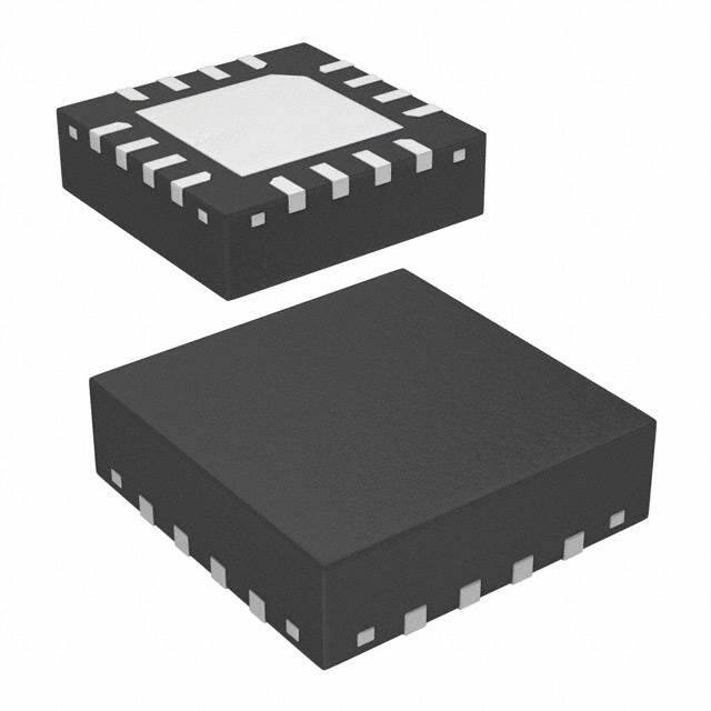
The RT9625 comes in a small footprint with WQFN-16L
4x4 package.
z
z
z
z
z
z
z
Drive Four N-MOSFETs for Two-Phase PWM Control
Shoot Through Protection
Embedded Bootstrap Diode
Support High Switching Frequency
Fast Output Rising Time
Tri-State PWM Input for Output Shutdown
Small 16-Lead WQFN Package
RoHS Compliant and Halogen Free
Applications
z
z
z
z
Core Voltage Supplies for Desktop, Motherboard CPU
High Frequency Low Profile DC/DC Converters
High Current Low Voltage DC/DC Converters
Core Voltage Supplies for GFX Card
Marking Information
09 : Product Code
YMDNN : Date Code
09 YM
DNN
Simplified Application Circuit
VIN
12V
VCC
RT9625B
L1
PHASE1
PWM1
PWM1
PWM2
PWM2
VOUT
L2
PHASE2
GND
Copyright © 2013 Richtek Technology Corporation. All rights reserved.
DS9625B-03
June 2013
is a registered trademark of Richtek Technology Corporation.
www.richtek.com
1
�RT9625B
Ordering Information
Pin Configurations
RT9625B
Note :
Richtek products are :
LGATE2
GND
Lead Plating System
Z : ECO (Ecological Element with
Halogen Free and Pb free)
PHASE2
Package Type
QW : WQFN-16L 4x4 (W-Type)
UGATE2
(TOP VIEW)
16
15
14
13
BOOT2
1
12
VCC
11
LGATE1
10
PHASE1
9
UGATE1
GND
2
PWM2
3
NC
4
GND
`
Suitable for use in SnPb or Pb-free soldering processes.
5
6
7
POR
ments of IPC/JEDEC J-STD-020.
8
BOOT1
RoHS compliant and compatible with the current require-
PWM1
`
NC
17
WQFN-16L 4x4
Function Pin Description
Pin No.
Pin Name
1
BOOT2
8
BOOT1
2,
13 (Exposed Pad)
GND
3
PWM2
6
PWM1
4, 5
Pin Function
Bootstrap Power Pins for Channel 2 and Channel 1. This pin powers the high
side MOSFET driver. Connect this pin to the junction of the bootstrap
capacitor and the cathode of the bootstrap diode.
Ground. The exposed pad must be soldered to a large PCB and connected to
GND for maximum power dissipation.
PWM Signal Input. Connect this pin to the PWM output of the controller.
NC
No Internal Connection.
7
POR
Power On Reset Signal.
9
UGATE1
16
UGATE2
High Side Gate Drive Outputs for channel 1 and channel 2. Connect this pin
to Gate of high side power MOSFET.
10
PHASE1
15
PHASE2
11
LGATE1
14
LGATE2
12
VCC
Switch Nodes of High Side Driver 1 and Driver 2. Connect this pin to the high
side MOSFET Source together with the low side MOSFET Drain and the
inductor.
Low Side Gate Drive Output for Channel 1 and Channel 2. This pin drives the
Gate of low side MOSFET.
Supply Input. VCC supplies current for Channel 1 and Channel 2 gate
drivers.
Copyright © 2013 Richtek Technology Corporation. All rights reserved.
www.richtek.com
2
is a registered trademark of Richtek Technology Corporation.
DS9625B-03
June 2013
�RT9625B
Function Block Diagram
VCC
POR
Bootstrap
Control
POR
BOOT1
Internal
VDD
Tri-State
Detect
PWM1
Shoot-Through
Protection
UGATE1
Turn Off
Detection
PHASE1
VCC
Shoot-Through
Protection
LGATE1
GND
VCC1
Bootstrap
Control
BOOT2
Internal
VDD
Tri-State
Detect
PWM2
Shoot-Through
Protection
UGATE2
Turn Off
Detection
PHASE2
VCC
Shoot-Through
Protection
LGATE2
GND
Copyright © 2013 Richtek Technology Corporation. All rights reserved.
DS9625B-03
June 2013
is a registered trademark of Richtek Technology Corporation.
www.richtek.com
3
�RT9625B
Operation
POR (Power On Reset)
Bootstrap Control
POR block detects the voltages at VCC pin. When the
VCC pin voltage is higher than POR rising threshold, POR
pin output voltage (POR output) is high. POR output is
low when VCC is not higher than POR rising threshold.
When the POR pin voltage is high, UGATEx and LGATEx
can be controlled by PWMx input voltage. If the POR pin
voltage is low, both UGATEx and LGATEx will be pulled
to low.
Bootstrap control block controls the integrated bootstrap
switch. When LGATEx is high (low side MOSFET is
turned on), the bootstrap switch is turned on to charge
the bootstrap capacitor connected to BOOTx pin. When
LGATEx is low (low side MOSFET is turned off), the
bootstrap switch is turned off to disconnect VCC pin and
BOOTx pin.
Turn-Off Detection
Tri-State Detect
When both POR block output and ENx pin voltages are
high, UGATEx and LGATEx can be controlled by PWMx
input. There are three PWMx input modes, which are high,
low, and shutdown state. If PWMx input is within the
shutdown window, both UGATEx and LGATEx output are
low. When PWMx input is higher than its rising threshold,
UGATEx is high and LGATEx is low. When PWMx input
is lower than its falling threshold, UGATEx is low and
LGATEx is high.
Copyright © 2013 Richtek Technology Corporation. All rights reserved.
www.richtek.com
4
Turn-off detection block detects whether high side
MOSFET is turned off by monitoring PHASEx pin voltage.
To avoid shoot through between high side and low side
MOSFETs, low side MOSFET can be turned on only after
high side MOSFET is effectively turned off.
Shoot-Through Protection
Shoot-through protection block implements the dead time
when both high side and low side MOSFETs are turned
off. With shoot-through protection block, high side and
low side MOSFET are never turned on simultaneously.
Thus, shoot through between high side and low side
MOSFETs is prevented.
is a registered trademark of Richtek Technology Corporation.
DS9625B-03
June 2013
�RT9625B
Absolute Maximum Ratings
z
z
z
z
z
z
z
z
z
z
z
z
z
(Note 1)
Supply Voltage, VCC -------------------------------------------------------------------------------- −0.3V to 15V
BOOTx to PHASEx ---------------------------------------------------------------------------------- −0.3V to 15V
PHASEx to GND
DC -------------------------------------------------------------------------------------------------------- −0.3V to 30V
< 20ns --------------------------------------------------------------------------------------------------- −10V to 35V
LGATEx to GND
DC -------------------------------------------------------------------------------------------------------- −0.3V to (VCC + 0.3V)
< 20ns --------------------------------------------------------------------------------------------------- −2V to (VCC + 0.3V)
UGATEx to GND
DC -------------------------------------------------------------------------------------------------------- (VPHASE − 0.3V) to (VBOOT + 0.3V)
< 20ns --------------------------------------------------------------------------------------------------- (VPHASE − 2V) to (VBOOT + 0.3V)
PWMx to GND ---------------------------------------------------------------------------------------- −0.3V to 7V
POR to GND ------------------------------------------------------------------------------------------- −0.3V to 5V
Power Dissipation, PD @ TA = 25°C
WQFN-16L 4x4 --------------------------------------------------------------------------------------- 1.852W
Package Thermal Resistance (Note 2)
WQFN-16L 4x4, θJA ---------------------------------------------------------------------------------- 54°C/W
WQFN-16L 4x4, θJC --------------------------------------------------------------------------------- 7°C/W
Lead Temperature (Soldering, 10 sec.) ---------------------------------------------------------- 260°C
Junction Temperature -------------------------------------------------------------------------------- 150°C
Storage Temperature Range ----------------------------------------------------------------------- −65°C to 150°C
ESD Susceptibility (Note 3)
HBM (Human Body Model) ------------------------------------------------------------------------- 2kV
Recommended Operating Conditions
z
z
z
z
(Note 4)
Supply Voltage, VCC -------------------------------------------------------------------------------- 4.5V to 13.2V
Input Voltage, (VIN + VCC) ------------------------------------------------------------------------- < 35V
Junction Temperature Range ----------------------------------------------------------------------- −40°C to 125°C
Ambient Temperature Range ----------------------------------------------------------------------- −40°C to 85°C
Electrical Characteristics
(VCC = 12V, TA = 25°C unless otherwise specified)
Parameter
Symbol
Test Conditions
Min
Typ
Max
Unit
4.5
--
13.2
V
Power Supply Voltage
VCC
Power Supply Current
I VCC
VBOOTx = 12V, PWMx Floating
--
180
--
μA
POR Rising Threshold
VPOR_r
VCC Rising
--
4
4.4
V
POR Falling Threshold
VPOR_f
VCC Falling
3
3.5
--
V
POR Pin High Voltage
VPOR_H
--
3.5
4
V
POR Pin Low Voltage
VPOR_L
--
--
0.5
V
Power On Reset (POR)
Copyright © 2013 Richtek Technology Corporation. All rights reserved.
DS9625B-03
June 2013
is a registered trademark of Richtek Technology Corporation.
www.richtek.com
5
�RT9625B
Parameter
Symbol
Test Conditions
Min
Typ
Max
Unit
PWM Input
Maximum Input Current
IPWM
VPWMx = 0V or 5V
--
160
--
μA
PWMx Floating Voltage
VPWM_fl
PWMx = Open
--
1.8
--
V
PWMx Rising Threshold
VPWM_rth
2.3
2.8
3.2
V
PWMx Falling Threshold
VPWM_fth
0.7
1.1
1.4
V
Timing
UGATEx Rising Time
tUGATEr
3nF load
--
25
--
ns
UGATEx Falling Time
tUGATEf
3nF load
--
12
--
ns
LGATEx Rising Time
tLGATEr
3nF load
--
24
--
ns
LGATEx Falling Time
tLGATEf
3nF load
--
10
--
ns
tUGATEpdh
VBOOTx − VPHASEx = 12V
See Timing Diagram
--
60
--
--
22
--
--
30
--
--
8
--
Propagation Delay
tUGATEpdl
tLGATEpdh
tLGATEpdl
See Timing Diagram
ns
ns
Output
UGATEx Drive Source
RUGATEsr
VBOOT − VPHASE = 12V, I Source = 100mA
--
1.7
--
Ω
UGATEx Drive Sink
RUGATEsk
VBOOT − VPHASE = 12V, I Sink = 100mA
--
1.4
--
Ω
LGATEx Drive Source
RLGATEsr
ISource = 100mA
--
1.6
--
Ω
LGATEx Drive Sink
RLGATEsk
ISink = 100mA
--
1.1
--
Ω
Note 1. Stresses beyond those listed “Absolute Maximum Ratings” may cause permanent damage to the device. These are
stress ratings only, and functional operation of the device at these or any other conditions beyond those indicated in
the operational sections of the specifications is not implied. Exposure to absolute maximum rating conditions may
affect device reliability.
Note 2. θJA is measured at TA = 25°C on a high effective thermal conductivity four-layer test board per JEDEC 51-7. θJC is
measured at the exposed pad of the package.
Note 3. Devices are ESD sensitive. Handling precaution is recommended.
Note 4. The device is not guaranteed to function outside its operating conditions.
Copyright © 2013 Richtek Technology Corporation. All rights reserved.
www.richtek.com
6
is a registered trademark of Richtek Technology Corporation.
DS9625B-03
June 2013
�RT9625B
Typical Application Circuit
RT9625B
12V
R1
2.2
12 VCC2
C1
1µF
BOOT1 8
UGATE1
PHASE1
7
POR
LGATE1
6
PWM1
PWM1
3 PWM2
PWM2
C3
1µF
9
R3
2.2
VIN
12V
C2
270µF x 2
Q1
L1
10
R4
0
11
BOOT2 1
UGATE2
R2
1
16
R6
1
C6
1µF
R7
2.2
Q2
C4
3.3nF
VIN
Q3
L2
PHASE2 15
2, 13, 17 (Exposed Pad)
GND
LGATE2
14
VOUT
C5
820µF x 3
R5
2.2
R8
0
R9
2.2
Q4
C7
3.3nF
Timing Diagram
PWMx
LGATEx
tLGATEpdl
90%
tUGATEpdl
1.5V
1.5V
1.5V
90%
1.5V
UGATEx
tUGATEpdh
Copyright © 2013 Richtek Technology Corporation. All rights reserved.
DS9625B-03
June 2013
tLGATEpdh
is a registered trademark of Richtek Technology Corporation.
www.richtek.com
7
�RT9625B
Typical Operating Characteristics
PWM Rising Edge
PWM Falling Edge
PWM
(10V/Div)
PWM
(10V/Div)
UGATE
(20V/Div)
UGATE
(20V/Div)
LGATE
(10V/Div)
LGATE
(10V/Div)
PHASE
(10V/Div)
PHASE
(10V/Div)
Time (20ns/Div)
Time (20ns/Div)
Dead Time
Dead Time
UGATE
UGATE
PHASE
PHASE
LGATE
LGATE
(5V/Div)
(5V/Div)
Full Load
Full Load
Time (20ns/Div)
Time (20ns/Div)
Dead Time
Dead Time
UGATE
UGATE
PHASE
PHASE
LGATE
(5V/Div)
LGATE
(5V/Div)
No Load
Time (20ns/Div)
Copyright © 2013 Richtek Technology Corporation. All rights reserved.
www.richtek.com
8
No Load
Time (20ns/Div)
is a registered trademark of Richtek Technology Corporation.
DS9625B-03
June 2013
�RT9625B
Short Pulse
UGATE
LGATE
PHASE
(5V/Div)
UGATE − PHASE
No Load
Time (20ns/Div)
Copyright © 2013 Richtek Technology Corporation. All rights reserved.
DS9625B-03
June 2013
is a registered trademark of Richtek Technology Corporation.
www.richtek.com
9
�RT9625B
Application Information
The RT9625B is a high frequency, two-channel
synchronous rectified MOSFET driver containing Richtek's
advanced MOSFET driver technologies. The RT9625B is
designed to be able to adapt from normal MOSFET driving
applications to high performance CPU VR driving
capabilities.
Bootstrap Power Switch
Supply Voltage and Power On Reset
Non-overlap Control
The RT9625B can be utilized under both VCC = 5V or VCC
= 12V applications which may happen in different fields of
electronics application circuits. In terms of efficiency,
higher VCC equals higher driving voltage of UGATEx/
LGATEx which may result in higher switching loss and
lower conduction loss of power MOSFETs. The choice of
VCC = 12V or VCC = 5V can be a tradeoff to optimize
system efficiency.
To prevent the overlap of the gate drivers during the
UGATEx pull low and the LGATEx pull high, the non-overlap
circuit monitors the voltages at the PHASEx node and
high side gate drive (UGATEx − PHASEx). When the
PWMx input signal goes low, UGATEx begins to pull low
(after propagation delay). Before LGATEx is pulled high,
the non-overlap protection circuit ensures that the
monitored voltages have gone below 1.1V. Once the
monitored voltages fall below 1.1V, LGATEx begins to turn
high. By waiting for the voltages of the PHASEx pin and
high side gate driver to fall below 1.1V, the non-overlap
protection circuit ensures that UGATEx is low before
LGATEx pulls high.
The RT9625B controls both high side and low side NMOSFETs of two half-bridge power according to two
external input PWMx control signals. It has Power On
Reset (POR) function which held UGATEx and LGATEx
low before the VCC voltage rises to higher than rising
threshold voltage. When VCC exceeds the POR threshold
voltage, the voltage at the POR pin will be pulled high.
Tri-state PWM Input
After the initialization, the PWMx signal takes the control.
The rising PWMx signal first forces the LGATEx signal to
turn low then UGATEx signal is allowed to go high just
after a non-overlapping time to avoid shoot through current.
The falling of PWMx signal first forces UGATEx to go low.
When UGATEx and PHASEx signal reach a
predetermined low level, LGATEx signal is allowed to turn
high.
The PWMx signal is acted as “ High” if the signal is above
the rising threshold and acted as “ Low” if the signal is
below the falling threshold. When PWM signal level enters
and remains within the shutdown window, the output drivers
are disabled and both MOSFET gates are pulled and held
low. If the PWMx signal is left floating, the pin will be kept
around 1.8V by the internal divider and provide the PWMx
controller with a recognizable level.
Copyright © 2013 Richtek Technology Corporation. All rights reserved.
www.richtek.com
10
The RT9625B builds in internal bootstrap power switches
to replace external bootstrap diode, and this can facilitate
PCB design and reduce total BOM cost of the system.
Hence, no external bootstrap diode is required in real
applications.
Also to prevent the overlap of the gate drivers during
LGATEx pull low and UGATEx pull high, the non-overlap
circuit monitors the LGATEx voltage. When LGATEx goes
below 1.1V, UGATEx goes high after propagation delay.
Driving Power MOSFETs
The DC input impedance of the power MOSFET is
extremely high. When Vgs1 or Vgs2 is at 12V or 5V, the
gate draws the current only for few nano-amperes. Thus
once the gate has been driven up to “ ON” level, the
current could be negligible.
However, the capacitance at the gate to source terminal
should be considered. It requires relatively large currents
to drive the gate up and down 12V (or 5V) rapidly. It is
also required to switch drain current on and off with the
required speed. The required gate drive currents are
calculated as follows.
is a registered trademark of Richtek Technology Corporation.
DS9625B-03
June 2013
�RT9625B
d1
s1
VPHASEx
VIN
L
VOUT
Cgs1
Cgd1
Cgd2
Igs1
Igd1
Ig1
g1
low side is turned on. From Figure 1, the body diode “ D2”
will be turned on before high side MOSFETs turn on.
dV
12
Igd1 = Cgd1
= Cgd1
(3)
dt
tr1
d2
Ig2 Igd2
g2
D2
Igs2
Cgs2
s2
GND
Vg1
Before the low side MOSFET is turned on, the Cgd2 have
been charged to VIN. Thus, as Cgd2 reverses its polarity
and g2 is charged up to 12V, the required current is
Igd2 = Cgd2
VPHASEx +12V
12V
t
Figure 1. Equivalent Circuit and Waveforms (VCC = 12V)
Igs1 =
In Figure 1, the current Ig1 and Ig2 are required to move the
gate up to 12V. The operation consists of charging Cgd1,
Cgd2 , Cgs1 and Cgs2. Cgs1 and Cgs2 are the capacitors from
gate to source of the high side and the low side power
MOSFETs, respectively. In general data sheets, the Cgs1
and C gs2 are referred as “ Ciss” which are the input
capacitors. Cgd1 and Cgd2 are the capacitors from gate to
drain of the high side and the low side power MOSFETs,
respectively and referred to the data sheets as “ Crss” the
reverse transfer capacitance. For example, tr1 and tr2 are
the rising time of the high side and the low side power
MOSFETs respectively, the required current Igs1 and Igs2,
are shown as below :
dVg1 Cgs1 x 12
(1)
Igs1 = Cgs1
=
dt
tr1
Igs2 =
Igs2 = Cgs1
dVg2
dt
=
Cgs1 x 12
(4)
1660 x 10-12 x 12
14 x 10-9
2200 x 10-12 x 12
30 x 10-9
= 1.428
= 0.88
(5)
(A)
(A)
(6)
from equation. (3) and (4)
Igd1 =
Igd2 =
380 x 10-12 x 12
14 x 10-9
= 0.326 (A)
500 x 10-12 x (12+12 )
30 x 10
-9
(7)
= 0.4 (A)
(8)
the total current required from the gate driving source can
be calculated as following equations.
Ig1 = Igs1 + Igd1 = (1.428 + 0.326 ) = 1.754 (A)
Ig2 = Igs2 + Igd2 = ( 0.88 + 0.4 ) = 1.28 (A)
(9)
(10)
By a similar calculation, we can also get the sink current
required from the turned off MOSFET.
(2)
tr2
Copyright © 2013 Richtek Technology Corporation. All rights reserved.
DS9625B-03
VIN + 12
dV
= Cgd2
dt
tr2
It is helpful to calculate these currents in a typical case.
Assume a synchronous rectified Buck converter, input
voltage VIN = 12V, Vgs1 = 12V, Vgs2 = 12V.The high side
MOSFET is PHB83N03LT whose C iss = 1660pF,
Crss = 380pF, and tr = 14ns. The low side MOSFET is
PHB95N03LT whose Ciss = 2200pF, Crss = 500pF and
tr = 30ns, from the equation (1) and (2) we can obtain
t
Vg2
Before driving the gate of the high side MOSFET up to
12V, the low side MOSFET has to be off; and the high
side MOSFET will be turned off before the
June 2013
is a registered trademark of Richtek Technology Corporation.
www.richtek.com
11
�RT9625B
CBOOT
1µF
Select the Bootstrap Capacitor
Figure 2 shows part of the bootstrap circuit of the
RT9625B. The VCB (the voltage difference between BOOTx
and PHASEx on RT9625B) provides a voltage to the gate
of the high side power MOSFET. This supply needs to be
ensured that the MOSFET can be driven. For this, the
capacitance CBOOT has to be selected properly. It is
determined by the following constraints.
10
12V
1µF
BOOTx
UGATEx
VCC
2N7002
RT9625B
CU
3nF
POR
POR
12V
PHASEx
2N7002
PWNx
PWMx
VIN
20
LGATEx
GND
CL
3nF
BOOTx
UGATEx
PHASEx
CBOOT
Figure 3. Power Dissipation Test Circuit
+
VCB
-
VCC
LGATEx
GND
Figure 4 shows the power dissipation of the RT9625B as
a function of frequency and load capacitance when VCC =
12V. The value of CU and CL are the same and the frequency
is varied from 100kHz to 1MHz.
Power Dissipation vs. Frequency
1000
Figure 2. Part of Bootstrap Circuit of RT9625B
Power Dissipation
To prevent driving the IC beyond the maximum
recommended operating junction temperature of 125°C,
it is necessary to calculate the power dissipation
appropriately. This dissipation is a function of switching
frequency and total gate charge of the selected MOSFET.
Figure 3 shows the power dissipation test circuit. CL and
C U are the UGATEx and LGATEx load capacitors,
respectively. The bootstrap capacitor value is 1μF.
Power Dissipation (mW)
In practice, a low value capacitor CBOOT will lead to the
over charging that could damage the IC. Therefore, to
minimize the risk of overcharging and to reduce the ripple
on VCB, the bootstrap capacitor should not be smaller than
0.1μF, and the larger the better. In general design, using
1μF can provide better performance. At least one low-ESR
capacitor should be used to provide good local de-coupling.
It is recommended to adopt a ceramic or tantalum
capacitor.
900
800
CU = CL = 3nF
700
600
CU = CL = 2nF
500
400
300
200
CU = CL = 1nF
100
VCC = 12V
0
0
200
400
600
800
1000
Frequency (kHz)
Figure 4. Power Dissipation vs. Frequency
The operating junction temperature can be calculated from
the power dissipation curves (Figure 4). Assume VCC =
12V, operating frequency is 200kHz and CU = CL = 1nF
which emulate the input capacitances of the high side
and low side power MOSFETs. From Figure 4, the power
dissipation is 100mW. Thus, for example, with the SOP8 package, the package thermal resistance θJA is 120°C/
W. The operating junction temperature is then calculated
as :
TJ = (120°C/W x 100mW) + 25°C = 37°C
(11)
where the ambient temperature is 25°C.
Copyright © 2013 Richtek Technology Corporation. All rights reserved.
www.richtek.com
12
is a registered trademark of Richtek Technology Corporation.
DS9625B-03
June 2013
�RT9625B
Thermal Considerations
Layout Consideration
For continuous operation, do not exceed absolute
maximum junction temperature. The maximum power
dissipation depends on the thermal resistance of the IC
package, PCB layout, rate of surrounding airflow, and
difference between junction and ambient temperature. The
maximum power dissipation can be calculated by the
following formula :
Figure 6 shows the schematic circuit of a synchronous
buck converter to implement the RT9625B. The converter
operates from 5V to 12V of input Voltage.
PD(MAX) = (TJ(MAX) − TA) / θJA
where TJ(MAX) is the maximum junction temperature, TA is
the ambient temperature, and θJA is the junction to ambient
thermal resistance.
For recommended operating condition specifications of
the RT9625B, the maximum junction temperature is 125°C.
The junction to ambient thermal resistance, θJA, is layout
dependent. For WQFN-16L 4x4 packages, the thermal
resistance, θJA, is 54°C/W on a standard JEDEC 51-7
Next, the trace from UGATEx, and LGATEx should also
be short to decrease the noise of the driver output signals.
PHASEx signals from the junction of the power MOSFET,
carrying the large gate drive current pulses, should be as
heavy as the gate drive trace. The bypass capacitor CVCC
should be connected to GND directly. Furthermore, the
bootstrap capacitors (CBOOTx) should always be placed as
close to the pins of the IC as possible.
VIN
12V
LIN
12V
+
four-layer thermal test board. The maximum power
dissipation at TA = 25°C can be calculated by the following
formula :
For the PCB layout, it should be very careful. The power
circuit section is the most critical one. If not configured
properly, it will generate a large amount of EMI. The location
of QUGx, QLGx, Lx should be very close.
CIN
CIN2
RVCC
CBOOTx
PD(MAX) = (125°C - 25°C) / (54°C/W) = 1.852W for
WQFN-16L 4x4 package
Maximum Power Dissipation (W)
2.0
Four-Layer PCB
VCC
RT9625B
PHASEx
COUT
QLGx
CVCC
UGATEx
PHB83N03LT
+
The maximum power dissipation depends on the operating
ambient temperature for fixed T J(MAX) and thermal
resistance, θJA. The derating curve in Figure 5 allows the
designer to see the effect of rising ambient temperature
on the maximum power dissipation.
QUGx
Lx
VOUT
BOOTx
PHB95N03LT LGATEx
PWMx
PWMx
GND
Figure 6. Synchronous Buck Converter Circuit
1.8
1.6
1.4
1.2
1.0
0.8
0.6
0.4
0.2
0.0
0
25
50
75
100
125
Ambient Temperature (°C)
Figure 5. Derating Curve of Maximum Power Dissipation
Copyright © 2013 Richtek Technology Corporation. All rights reserved.
DS9625B-03
June 2013
is a registered trademark of Richtek Technology Corporation.
www.richtek.com
13
�RT9625B
Outline Dimension
D
SEE DETAIL A
D2
L
1
E
E2
e
b
A
A1
1
1
2
2
DETAIL A
Pin #1 ID and Tie Bar Mark Options
A3
Note : The configuration of the Pin #1 identifier is optional,
but must be located within the zone indicated.
Symbol
Dimensions In Millimeters
Dimensions In Inches
Min
Max
Min
Max
A
0.700
0.800
0.028
0.031
A1
0.000
0.050
0.000
0.002
A3
0.175
0.250
0.007
0.010
b
0.250
0.380
0.010
0.015
D
3.950
4.050
0.156
0.159
D2
2.000
2.450
0.079
0.096
E
3.950
4.050
0.156
0.159
E2
2.000
2.450
0.079
0.096
e
L
0.650
0.500
0.026
0.600
0.020
0.024
W-Type 16L QFN 4x4 Package
Richtek Technology Corporation
5F, No. 20, Taiyuen Street, Chupei City
Hsinchu, Taiwan, R.O.C.
Tel: (8863)5526789
Richtek products are sold by description only. Richtek reserves the right to change the circuitry and/or specifications without notice at any time. Customers should
obtain the latest relevant information and data sheets before placing orders and should verify that such information is current and complete. Richtek cannot
assume responsibility for use of any circuitry other than circuitry entirely embodied in a Richtek product. Information furnished by Richtek is believed to be
accurate and reliable. However, no responsibility is assumed by Richtek or its subsidiaries for its use; nor for any infringements of patents or other rights of third
parties which may result from its use. No license is granted by implication or otherwise under any patent or patent rights of Richtek or its subsidiaries.
www.richtek.com
14
DS9625B-03
June 2013
�


 工商网监
湘ICP备2023018690号
工商网监
湘ICP备2023018690号
