®
RTQ8577B
High Voltage 4-CH LED Driver
General Description
Features
The RTQ8577B is an 4-CH LED driver capable of delivering
120mA for each channel. The RTQ8577B is a current mode
boost converter with an adjustable switching frequency
via the RT pin from 200kHz to 2.1MHz and a wide VIN
range from 5.5V to 40V.
Wide Input Supply Voltage Range : 5.5V to 40V
Adjustable Boost Controller Switching Frequency
from 200kHz to 2.1MHz
Programmable Channel Current
Channel Current Matching : ±1.5%
External Dimming Control
Boost MOSFET Over Current Protection
Automatic LED Open/Short Protection to Avoid
Output Over Voltage
VCC Under Voltage Lockout
Adjustable Over Voltage Protection
Thermal Shutdown Protection
Abnormal Status Indicator for OVP/Short/OTP
Condition
AEC-Q100 Grade 2 Certification
RoHS Compliant and Halogen Free
Applications
RTQ8577B
Package Type
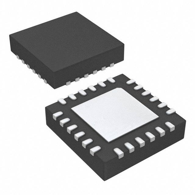
QW : WQFN-20L 5x5 (W-Type)
Lead Plating System
G : Green (Halogen Free and Pb Free)
Pin Configuration
(TOP VIEW)
Suitable for use in SnPb or Pb-free soldering processes.
Marking Information
RTQ8577BGQW : Product Number
YMDNN : Date Code
20
19
18
17
16
GND
1
15
STATUS
GND
2
14
VCC
GND
3
13
NC
LED3
4
12
CREG
LED4
5
11
DRV
GND
21
6
OVP
RTQ8577B
GQW
YMDNN
VC
ments of IPC/JEDEC J-STD-020.
PWM
RoHS compliant and compatible with the current require-
NC
LED1
Richtek products are :
LED2
Note :
7
8
9
10
EN
Ordering Information
Automotive Infotainment
LCD TV, Monitor Display Backlight
LED Driver Application
General Purpose Constant Current Source
SEN
When an abnormal situation (OVP/short/OTP) occurs, a
status signal will be sent to the system to shut down the
IC.
RT
matched LED currents on all channels are simply
programmed with a resistor. A very high contrast ratio true
digital PWM dimming can be achieved by driving the PWM
pin with a PWM signal.
RISET
The PWM output voltage loop selects and regulates the
LED pin with the highest voltage string to 0.6V, hence
allowing voltage mismatches between LED strings. The
RTQ8577B automatically detects and disconnects any
unconnected and/or broken strings during operation from
PWM loop to prevent VOUT from over voltage. The 1.5%
WQFN-20L 5x5
Copyright © 2016 Richtek Technology Corporation. All rights reserved.
DSQ8577B-00
December 2016
is a registered trademark of Richtek Technology Corporation.
www.richtek.com
1
�RTQ8577B
Functional Pin Description
Pin No.
Pin Name
1, 2, 3,
GND
21 (Exposed pad)
4, 5
LED4, LED3
Pin Function
Ground. The exposed pad must be soldered to a large PCB and connected to
GND for maximum power dissipation.
Channel 3 and channel 4 LED current sinks. Leave the pins unconnected if not
used.
Over-voltage detection input. The Boost converter turns off when VOVP goes
higher than 2V.
6
OVP
7
RISET
LED current set pin. a resistor or a current from DAC on this pin programs the
full LED current.
8
RT
Switching frequency set. Connect a resistor between RT and GND to set the
boost converter switching frequency.
9
EN
Enable control input. When EN is pulled low, the chip will be shut down.
10
SEN
Current sense input. During normal operation, this pin senses the voltage
across the external inductor current sensing resistor for peak current mode
control and also to limit the inductor current during every switching cycle.
11
DRV
Boost converter power switch gate output. This pin drives the external power
N-MOSFET device.
12
CREG
Regulator output for chip internal use only. A 1F capacitor should be placed on
this pin to stabilize the 5V output of the internal regulator.
NC
No internal connection.
14
VCC
Power supply of the chip. For good bypass, a low ESR capacitor close to the pin
is required.
15
STATUS
Status indicator output. This pin will be pulled to low if fault happens.
16
VC
PWM boost converter loop compensation node.
17
PWM
Dimming control input.
19
LED1
Channel 1 LED current sink, leave this pin unconnected if it is not used.
20
LED2
Channel 2 LED current sink, leave this pin unconnected if it is not used.
13, 18
Copyright © 2016 Richtek Technology Corporation. All rights reserved.
www.richtek.com
2
is a registered trademark of Richtek Technology Corporation.
DSQ8577B-00
December 2016
�RTQ8577B
Functional Block Diagram
DRV SEN
OSC
RT
VCC
STATUS
OVP
-
UVLO
S
+
OTP
R
OVP
+
2V
LED Short
R
-
LED1
-
1.2V
+
+
-
Shutdown
+
-
CREG
5V
LDO
VC
5V
VOUT
Regulation
Unit
PWM
…………………
EN
LED4
+
-
+
GND
-
RISET
Operation
The RTQ8577B integrated a current-mode Boost PWM
controller and 4 LED drivers. When EN and PWM are high
and VIN is higher than the UVLO threshold voltage, the
controller starts operation. In normal operation, the DRV
pin turns high when the gate driver is set by the oscillator
and the DRV pin turns low when the gate driver is reset by
the current comparator. When the DRV pin turns high to
turn on the external MOSFET, the inductor current will
rise up. Once the SEN pin voltage reaches the level of the
VC pin, the current comparator will reset the gate driver
and turn off the MOSFET. The DRV pin is then set to high
again by OSC and repeats in the next switching cycle.
The oscillator frequency can be set by an external resistor
at the RT pin.
Copyright © 2016 Richtek Technology Corporation. All rights reserved.
DSQ8577B-00
December 2016
The output voltage of the Boost converter supports LED
current and regulation voltage at the LEDx pin. The LED
current is set by an external resistor at the RISET pin. A
PWM dimming function is provided to control the LED
brightness through the PWM pin. If OVP, OTP or shorted
LED happens, the STATUS pin will be pulled to low as a
fault indicator.
is a registered trademark of Richtek Technology Corporation.
www.richtek.com
3
�RTQ8577B
Absolute Maximum Ratings
(Note 1)
Supply Voltage, VCC, STATUS ----------------------------------------------------------------------------------------LED1 to LED4 --------------------------------------------------------------------------------------------------------------PWM, EN, DRV, SEN, VC, RT, CREG, OVP, RISET -------------------------------------------------------------Power Dissipation, PD @ TA = 25°C
WQFN-20L 5x5 ------------------------------------------------------------------------------------------------------------Package Thermal Resistance (Note 2)
WQFN-20L 5x5, θJA -------------------------------------------------------------------------------------------------------WQFN-20L 5x5, θJC ------------------------------------------------------------------------------------------------------Junction Temperature -----------------------------------------------------------------------------------------------------Lead Temperature (Soldering, 10 sec.) -------------------------------------------------------------------------------Storage Temperature Range --------------------------------------------------------------------------------------------ESD Susceptibility (Note 3)
HBM (Human Body Model) ----------------------------------------------------------------------------------------------MM (Machine Model) ------------------------------------------------------------------------------------------------------
Recommended Operating Conditions
−0.3V to 45V
−0.3V to 50V
−0.3V to 5.6V
3.54W
28.2°C/W
7.1°C/W
150°C
260°C
−65°C to 150°C
2kV
200V
(Note 4)
Supply Voltage, VCC -----------------------------------------------------------------------------------------------------LED1 to LED4 --------------------------------------------------------------------------------------------------------------ILED1 to ILED4 ----------------------------------------------------------------------------------------------------------------Junction Temperature Range --------------------------------------------------------------------------------------------Ambient Temperature Range ---------------------------------------------------------------------------------------------
5.5V to 40V
45V
20mA to 120mA
−40°C to 125°C
−40°C to 105°C
Electrical Characteristics
(VCC = 12V, TA = −40°C to 105°C, unless otherwise specified)
Parameter
Symbol
Test Conditions
Min
Typ
Max
Unit
Supply Voltage
Supply Current
IVCC
Switching Off
--
5
--
mA
Shutdown Current
ISHDN
VEN 0.7V
--
10
--
A
VDD LDO Output
VCREG
4.5
5
5.5
V
VDD LDO Capability
ICREG
30
--
--
mA
VCC UVLO Threshold
VUVLO
VCC Rising
--
4.5
--
Hysteresis
--
0.3
--
EN Threshold
Voltage
Logic-High
VENH
1.5
--
--
Logic-Low
VENL
--
--
0.8
V
V
LED Current Programming
LED Current Accuracy
RISET = 15k, VPWM 1.2V
ILED = 80mA
ILED = (20mA, 120mA) (Note 5)
76
80
84
mA
LED Current Matching
ILEDx ILED_AVE
100%
ILED_AVE
--
1.5
3
%
Copyright © 2016 Richtek Technology Corporation. All rights reserved.
www.richtek.com
4
is a registered trademark of Richtek Technology Corporation.
DSQ8577B-00
December 2016
�RTQ8577B
Parameter
Symbol
Test Conditions
Min
Typ
Max
Unit
LED1 to LED4 Regulation
Voltage
ILED = 80mA
--
0.86
--
V
VLED Threshold
No Connection
--
0.1
--
V
--
1.2
--
V
RISET Pin Voltage
Dimming
Logic-High
VPWMH
1.2
--
--
Logic-Low
VPWML
--
--
0.52
RRT = 20k
1.8
2.1
2.4
MHz
RRT = Open
--
200
--
kHz
Working
--
40
60
ns
80
--
--
%
0.3
0.5
0.6
V
Gate Driver Source
0.9
2.5
3.5
A
Gate Driver Sink
1.6
3
7
A
1.9
2
2.1
V
PWM Threshold
Voltage
V
PWM Boost Controller
Switching Frequency
f SW
Minimum On Time
tON
Maximum Duty Cycle
Dmax
SEN Current Sense Limit
Input Current Limit
OVP, SCP, OTP
OVP Threshold
VOVP
SCP Threshold
VSCP
LED1 to LED4
--
7
--
V
Thermal Shutdown Temperature
TSD
Lockout Temperature Point
--
150
--
C
Thermal Shutdown Hysteresis
TSD
Resume Temperature Point
--
20
--
C
STATUS Low Voltage
VSTATUS
Open Drain at 1mA
--
--
0.5
V
Note 1. Stresses beyond those listed “Absolute Maximum Ratings” may cause permanent damage to the device. These are
stress ratings only, and functional operation of the device at these or any other conditions beyond those indicated in the
operational sections of the specifications is not implied. Exposure to absolute maximum rating conditions may affect
device reliability.
Note 2. θJA is measured under natural convection (still air) at TA = 25°C with the component mounted on a high effective-thermalconductivity four-layer test board on a JEDEC 51-7 thermal measurement standard. θJC is measured at the exposed pad
of the package.
Note 3. Devices are ESD sensitive. Handling precaution is recommended.
Note 4. The device is not guaranteed to function outside its operating conditions.
Note 5. The LED current matching at 20mA and 120mA is guaranteed by design and not production tested.
Copyright © 2016 Richtek Technology Corporation. All rights reserved.
DSQ8577B-00
December 2016
is a registered trademark of Richtek Technology Corporation.
www.richtek.com
5
�RTQ8577B
Typical Application Circuit
L1
10µH
VIN
5.5V to 40V
R1
D1
CIN
20µF
CVCC
1µF
MSW
RF1
100
RSENSE
100m
Enable
RC
560
CC
0.22µF
SEN
11 DRV
STATUS
RPWM
1k 17
PWM
RENA
1k
RISET
RT
9 EN
16
:
:
:
:
RSTATUS
100k
15
:
:
: …… :
:
:
:
:
:
:
:
:
COUT
4.7µF x 6
VIN
FLT
7
RISET
9.1k
8
RRT 56k
CREG 12
CREG 1µF
VC
GND
1, 2, 3,
21 (Exposed Pad)
ILED (Note 5)
RISET
120mA
10k
80mA
15k
20mA
68k
Copyright © 2016 Richtek Technology Corporation. All rights reserved.
www.richtek.com
6
19
LED1
20
LED2
4
LED3
5
LED4
CF
1nF
External PWM
ROVP1
100k
RTQ8577B
10
RDRV
5
ROVP2
2.1M
OVP 6
14 VCC
VOUT
45V (MAX)
is a registered trademark of Richtek Technology Corporation.
DSQ8577B-00
December 2016
�RTQ8577B
Timing Diagram
Power On/Off Sequence
LED driver is without power sequence concern. Mode1,
Mode2 and Mode3 are different power sequences
respectively. There is no concern in the above condition.
Mode1 : Delay Time of PWM vs VOUT
VIN
VOUT
EN
100ns
PWM
Mode2 : Delay Time of EN vs VOUT
VIN
VOUT
100µs
EN
PWM
Mode3 : Delay Time of VIN vs VOUT
VIN
UVLO
UVLO
VOUT
EN
PWM
Figure 1. Power On/Off Sequence
Copyright © 2016 Richtek Technology Corporation. All rights reserved.
DSQ8577B-00
December 2016
is a registered trademark of Richtek Technology Corporation.
www.richtek.com
7
�RTQ8577B
Typical Operating Characteristics
LED Current vs. Input Voltage
LED Current vs. PWM Duty Cycle
160
120
100
LED Current (mA)
LED Current (mA)
140
120
LED1
LED2
LED3
LED4
100
80
80
PWM = 200Hz
PWM = 1kHz
PWM = 10kHz
60
40
20
48LEDs, RISET = 10kΩ
VIN = 12V, 48LEDs, RISET = 10kΩ
60
0
8
10
12
14
16
18
20
22
24
26
28
0
10
20
30
40
50
60
70
80
90
Input Voltage (V)
PWM Duty Cycle (%)
Efficiency vs. Input Voltage
Start up with Minimum PWM Duty
100
100
Efficiency (%)
95
90
VOUT
(10V/Div)
85
VIN
(5V/Div)
80
IOUT
(50mA/Div)
75
PWM
(2V/Div)
48LEDs, RISET = 10kΩ
70
8
10
12
14
16
18
20
22
24
26
f = 400Hz, PWM Duty = 1%
Time (50ms/Div)
28
Input Voltage (V)
OVP Protection
LED Short Delay Time
VIN = 12V, Short 3LEDs,
48LEDs, RISET = 10kΩ
OVP
(1V/Div)
OVP Trigger by LED remove,
VIN = 12V, VOUT = 48LEDS
VLEDx
(10V/Div)
VOUT
(5V/Div)
STATUS
(5V/Div)
STATUS
(5V/Div)
DRV
(5V/Div)
DRV
(5V/Div)
Time (100μs/Div)
Copyright © 2016 Richtek Technology Corporation. All rights reserved.
www.richtek.com
8
IOUT
(100mA/Div)
Time (25μs/Div)
is a registered trademark of Richtek Technology Corporation.
DSQ8577B-00
December 2016
�RTQ8577B
LED Short Protection
LED Short Protection
IOUT
(100mA/Div)
IOUT
(100mA/Div)
STATUS
(5V/Div)
Before Short
STATUS
(5V/Div)
VLEDx
(10V/Div)
VLEDx
(10V/Div)
DRV
(5V/Div)
DRV
(5V/Div)
VIN = 12V, Short 3LEDs
Time (2.5ms/Div)
Power On from EN
Power Off from EN
EN
(2V/Div)
DRV
(5V/Div)
DRV
(5V/Div)
I IN
(1A/Div)
I IN
(1A/Div)
VIN = 12V, 48LEDs, RISET = 10kΩ
VIN = 12V, 48LEDs, RISET = 10kΩ
Time (10ms/Div)
Time (25ms/Div)
Power On from VIN
Power Off from VIN
VIN
(10V/Div)
VIN
(10V/Div)
DRV
(5V/Div)
DRV
(5V/Div)
VIN = 12V, 48LEDs, RISET = 10kΩ
Time (10ms/Div)
Copyright © 2016 Richtek Technology Corporation. All rights reserved.
DSQ8577B-00
VIN = 12V, Short 3LEDs
Time (2.5ms/Div)
EN
(2V/Div)
I IN
(1A/Div)
After Short
December 2016
I IN
(1A/Div)
VIN = 12V, 48LEDs, RISET = 10kΩ
Time (25ms/Div)
is a registered trademark of Richtek Technology Corporation.
www.richtek.com
9
�RTQ8577B
Power On from PWM
Power Off from PWM
PWM
(2V/Div)
PWM
(2V/Div)
DRV
(5V/Div)
DRV
(5V/Div)
I IN
(1A/Div)
I IN
(1A/Div)
VIN = 12V, 48LEDs, RISET = 10kΩ
Time (10ms/Div)
Copyright © 2016 Richtek Technology Corporation. All rights reserved.
www.richtek.com
10
VIN = 12V, 48LEDs, RISET = 10kΩ
Time (10ms/Div)
is a registered trademark of Richtek Technology Corporation.
DSQ8577B-00
December 2016
�RTQ8577B
Application information
The RTQ8577B is an 4-CH driver controller that delivers
well matched LED current to each channel of LED strings.
The external N-MOSFET current source will accommodate
the power dissipation difference among channels resulting
from the forward voltage difference between the LED
strings. With high speed current source N-MOSFET
drivers, the RTQ8577B features highly accurate current
matching, while also providing very fast turn-on and turnoff times. This allows a very narrow minimum on or off
pulse. The RTQ8577B integrates adjustable switching
frequency and provides circuitry for over temperature, over
voltage, under voltage and current limit protection.
Compensation
The regulator loop can be compensated by adjusting the
external components connected to the VC pin. The VC
pin is the output of the internal error amplifier. The
compensation capacitor will adjust the integrator zero to
maintain stability and the resistor value will adjust the
frequency integrator gain for fast transient response.
Typical values of the compensation components are RC =
560Ω, CC = 0.22μF.
LED Connection
The RTQ8577B equips 4-CH LED drivers and each channel
supports up to 15 LEDs. The LED strings are connected
from the output of the boost converter to pin LEDx (x = 1
to 4) respectively. If one of the LED channel is not in use,
the LED pin should be opened directly.
Setting and Regulation of LED current
The LED current can be calculated by the following
equation :
1200
ILED
40mA < ILED 120mA
RISET
ILED
1360
20mA < ILED 40mA
RISET
where RISET is the resistor between the RISET pin and
GND. This setting is the reference for the LED current at
pin LEDx and represents the sensed LED current for each
string. The DC/DC converter regulates the LED current
according to the setting.
Copyright © 2016 Richtek Technology Corporation. All rights reserved.
DSQ8577B-00
December 2016
Over Voltage Protection
The RTQ8577B integrates Over Voltage Protection (OVP)
. When the voltage at the OVP pin rises above the
threshold voltage of approximately 2V, the internal switch
will be turned off and STATUS pin will be pulled to low.
The internal switch will be turned on again once the voltage
at the OVP pin returns to normal range. The output voltage
can be clamped at a certain voltage level and can be
calculated by the following equations :
R
VOUT(OVP) = VOVP 1 + OVP2
ROVP1
where ROVP1 and ROVP2 are the resistors in the resistive
voltage divider connected to the OVP pin. If at least one
string is in normal operation, the controller will
automatically ignore the open strings and continue to
regulate the current for the strings in normal operation.
Suggested value for ROVP2 is up to 3.6MΩ to prevent loading
effect.
LED Short Circuit Protection
The RTQ8577B integrates LED Short Circuit Protection
(SCP). If one of the LED1 to LED4 pin voltages exceeds
a threshold of approximately 7V during normal operation,
the STATUS pin will be pulled low for a fault signal.
STATUS
The RTQ8577B provides a fault status indicator with an
open drain STATUS pin. If fault condition (LED Short/OVP/
OTP) occurs, the STATUS will be reset after VIN or EN is
re-applied.
Setting the Switching Frequency
The RTQ8577B switching frequency is programmable from
200kHz to 2.1MHz by adjusting the oscillator resistor,
RRT. The switching frequency can be calculated by the
following equation :
fSW 200k +
38 109
RRT
is a registered trademark of Richtek Technology Corporation.
www.richtek.com
11
�RTQ8577B
Current Limit Protection
Over Temperature Protection
The RTQ8577B can sense the RSENSE voltage between
the SEN pin and GND to achieve over current protection.
The boost converter senses the inductor current during
the on period. The duty cycle depends on the current
signal and internal slope compensation compared with
the error signal. The external switch will be turned off when
the current signal is larger than the internal slope
compensation. In the off period, the inductor current will
decrease until the internal switch is turned on by the
oscillator. The current limit value can be calculated by the
following equation :
0.5V
Current Limit (A)
RSENSE
The RTQ8577B has over temperature protection function
to prevent the IC from overheating due to excessive power
dissipation. The IC will shut down and the STATUS pin
will be pulled low when junction temperature exceeds
150°C. Main converter starts switching after junction
temperature cools down by approximately 20°C.
Inductor Selection
The value of the inductance, L, can be approximated by
the following equation, where the transition is from
Discontinuous Conduction Mode (DCM) to Continuous
Conduction Mode (CCM) :
2
L=
Brightness Control
The RTQ8577B features a digital dimming control scheme.
A very high contrast ratio true digital PWM dimming is
achieved by driving the PWM pin with a PWM signal. The
recommended PWM frequency is 100Hz to 10kHz, but
the LED current cannot be 100% proportional to duty cycle,
especially for high frequency and low duty ratio because
of physical limitation caused by inductor rising time.
Please refer to Table 1.
Table 1.
Dimming Frequency (Hz) Duty (Min.)
100 < f PWM 500
0.2%
500 < f PWM 1k
0.4%
1k < f PWM 2k
0.8%
2k < f PWM 5k
1.5%
5k < f PWM 10k
3%
Duty (Max.)
100%
100%
100%
100%
100%
Note : The minimum duty in Table 1 is based on the application
circuit and does not consider the deviation of current linearity.
Copyright © 2016 Richtek Technology Corporation. All rights reserved.
www.richtek.com
12
D 1 D VOUT
2 f IOUT
The duty cycle can be calculated as the following
equation :
V
VIN
D = OUT
VOUT
where VOUT is the maximum output voltage, VIN is the
minimum input voltage, f is the operating frequency, and
IOUT is the sum of current from all LED strings.
The boost converter operates in DCM over the entire input
voltage range when the inductor value is less than this
value, L. With an inductance greater than L, the converter
operates in CCM at the minimum input voltage and may
be discontinuous at higher voltages.
The inductor must be selected with a saturated current
rating that is greater than the peak current as provided by
the following equation :
V
I
V D T
IPEAK = OUT OUT IN
η VIN
2L
where η is the efficiency of the power converter.
is a registered trademark of Richtek Technology Corporation.
DSQ8577B-00
December 2016
�RTQ8577B
Schottky diodes are recommended for most applications
because of their fast recovery time and low forward voltage.
Power dissipation, reverse voltage rating, and pulsating
peak current are important parameters for consideration
when making a Schottky diode selection. Make sure that
the diode's peak current rating exceeds IPEAK and reverse
voltage rating exceeds the maximum output voltage.
Capacitor Selection
The input capacitor reduces current spikes from the input
supply and minimizes noise injection to the converter. For
general applications, six 4.7μF ceramic capacitors are
sufficient. A value higher or lower may be used depending
on the noise level from the input supply and the input
current to the converter.
WQFN-20L 5x5, the thermal resistance, θJA, is 28.2°C/W
on a standard JEDEC 51-7 high effective-thermalconductivity four-layer test board. The maximum power
dissipation at TA = 25°C can be calculated as below :
PD(MAX) = (125°C − 25°C / (28.2°C/W) = 3.54W for a
WQFN-20L 5x5 package.
The maximum power dissipation depends on the operating
ambient temperature for the fixed TJ(MAX) and the thermal
resistance, θJA. The derating curves in Figure 2 allows
the designer to see the effect of rising ambient temperature
on the maximum power dissipation.
4.0
Maximum Power Dissipation (W)1
Diode Selection
It is recommended to choose a ceramic capacitor based
on the output voltage ripple requirements. The minimum
value of the output capacitor, COUT, can be calculated by
the following equation :
COUT =
IOUT D
VOUT f
The junction temperature should never exceed the
absolute maximum junction temperature TJ(MAX), listed
under Absolute Maximum Ratings, to avoid permanent
damage to the device. The maximum allowable power
dissipation depends on the thermal resistance of the IC
package, the PCB layout, the rate of surrounding airflow,
and the difference between the junction and ambient
temperatures. The maximum power dissipation can be
calculated using the following formula :
For continuous operation, the maximum operating junction
temperature indicated under Recommended Operating
Conditions is 125°C. The junction-to-ambient thermal
resistance, θJA, is highly package dependent. For a
Copyright © 2016 Richtek Technology Corporation. All rights reserved.
DSQ8577B-00
December 2016
2.5
2.0
1.5
1.0
0.5
0
25
50
75
100
125
Ambient Temperature (°C)
Figure 2. Derating Curve of Maximum Power Dissipation
Layout Considerations
Careful PCB layout is very important for designing
switching power converter circuits. The following layout
guidelines should be strictly followed for best performance
of the RTQ8577B.
The power components L1, D1, CIN, COUT must be placed
as close as possible to the IC to reduce current loop.
The PCB trace between power components must be as
short and wide as possible.
The compensation circuit should be kept away from
the power loops and shielded with a ground trace to
prevent any noise coupling. Place the compensation
components, RC and CC, as close as possible to pin 9.
The exposed pad of the chip should be connected to
ground plane for thermal consideration.
PD(MAX) = (TJ(MAX) − TA) / θJA
where TJ(MAX) is the maximum junction temperature, TA is
the ambient temperature, and θJA is the junction-to-ambient
thermal resistance.
3.0
0.0
where ΔVOUT is the peak-to-peak ripple voltage at the
output.
Thermal Considerations
Four-Layer PCB
3.5
is a registered trademark of Richtek Technology Corporation.
www.richtek.com
13
�RTQ8577B
OVP Protection
VIN
PWM
Delay time 50µs
STATUS
Status latch until EN goes low
VOUT
OVP
2V
OVP
EN
SW Frequency = 2.1MHz
Time
DRV
Short Protection
VIN
PWM
ILEDX(1)
10µs
10µs
ILEDX(2)
Delay time 50µs
STATUS
Status latch until EN goes low
VLEDX(1)
LED SHORT
VLEDX(2)
EN
7V
SW Frequency = 2.1MHz
DRV
Copyright © 2016 Richtek Technology Corporation. All rights reserved.
www.richtek.com
14
Time
is a registered trademark of Richtek Technology Corporation.
DSQ8577B-00
December 2016
�RTQ8577B
OTP Function
130°C
150°C
Thermal
150°C
130°C
STATUS
VOUT
DRV
Protection Functions
Description
Detect VLEDx voltage.
Triggered if VLEDx 7V.
LED Short
Protection
Behavior
V
If one of LED1 to LED4 pin voltages exceeds a
threshold of approximately 7V during normal
operation, the STATUS pin will be pulled to low
for a fault signal. Internal switching does not stop.
OVP
Use OVP pin voltage for
detection. Triggered if OVP
pin voltage 2V.
V
OTP
Triggered if TJ 150C
V
STATUS pin is used as fault
indicator. Fault and pull low.
V
Fault Indicator
Copyright © 2016 Richtek Technology Corporation. All rights reserved.
DSQ8577B-00
December 2016
The internal switch will be turned off and
STATUS pin will be pulled to low.
The Internal switch will be turned on again once
the voltage at the OVP pin returns to normal
range.
The IC will shut down and the STATUS pin will
be pulled to low when junction temperature
exceeds 150C and IC returns to normal
operation when temperature falls to 130C.
If fault condition (LED short, OVP or OTP)
occurs, the STATUS pin will be pulled to low.
It will be reset after VIN or EN is re-applied.
is a registered trademark of Richtek Technology Corporation.
www.richtek.com
15
�RTQ8577B
Locate the CVCC as close to
VCC as possible.
CVCC
CC
PGND
LED1
NC
PWM
VC
20
19
18
17
16
VIN
GND
1
15
GND
2
14
STATUS
R1
VCC
GND
3
13
NC
LED3
4
12
CREG
LED4
5
11
DRV
GND
21
VIN
L1
RISET
9
D1
VOUT
MSW
10
CF
SEN
8
EN
7
RISET
RT
OVP
6
COUT
RDRV
RF1
AGND
CIN
+
Separate power ground (PGND) and
analog ground (AGND). Connect AGND
and PGND islands at a single end. Make
sure there are no other connections
between these separate ground planes.
The PGND should be wide and short
enough to connect ground plane.
LED2
RC
RSENSE
Place the power components as
Close as possible. The traces
should be wide and short especially
for the high current loop.
PGND
RRT
AGND
The exposed pad of the chip
should be connected to ground
plane for thermal consideration.
The compensation circuit and RISET resistor
should be kept away from the power loops and
should be shielded with a ground trace to prevent
any noise coupling.
Figure 3. PCB Layout Guide
Copyright © 2016 Richtek Technology Corporation. All rights reserved.
www.richtek.com
16
is a registered trademark of Richtek Technology Corporation.
DSQ8577B-00
December 2016
�RTQ8577B
Outline Dimension
1
2
DETAIL A
Pin #1 ID and Tie Bar Mark
Symbol
Dimensions In Millimeters
Dimensions In Inches
Min.
Max.
Min.
Max.
A
0.700
0.800
0.028
0.031
A1
0.000
0.050
0.000
0.002
A3
0.175
0.250
0.007
0.010
b
0.250
0.350
0.010
0.014
D
4.900
5.100
0.193
0.201
D2
3.100
3.200
0.122
0.126
E
4.900
5.100
0.193
0.201
E2
3.100
3.200
0.122
0.126
e
L
0.650
0.500
0.026
0.600
0.020
0.024
W-Type 20L QFN 5x5 Package
Copyright © 2016 Richtek Technology Corporation. All rights reserved.
DSQ8577B-00
December 2016
is a registered trademark of Richtek Technology Corporation.
www.richtek.com
17
�RTQ8577B
Footprint Information
Footprint Dimension (mm)
Package
Number of
Pin
P
Ax
Ay
Bx
By
C
D
Sx
Sy
V/W/U/XQFN5*5-20
20
0.65
5.80
5.80
3.80
3.80
1.00
0.40
3.25
3.25
Tolerance
±0.05
Richtek Technology Corporation
14F, No. 8, Tai Yuen 1st Street, Chupei City
Hsinchu, Taiwan, R.O.C.
Tel: (8863)5526789
Richtek products are sold by description only. Richtek reserves the right to change the circuitry and/or specifications without notice at any time. Customers should
obtain the latest relevant information and data sheets before placing orders and should verify that such information is current and complete. Richtek cannot
assume responsibility for use of any circuitry other than circuitry entirely embodied in a Richtek product. Information furnished by Richtek is believed to be
accurate and reliable. However, no responsibility is assumed by Richtek or its subsidiaries for its use; nor for any infringements of patents or other rights of third
parties which may result from its use. No license is granted by implication or otherwise under any patent or patent rights of Richtek or its subsidiaries.
www.richtek.com
18
DSQ8577B-00
December 2016
�


 工商网监
湘ICP备2023018690号
工商网监
湘ICP备2023018690号
