R1272S Series
34 V Input Synchronous Step-down DC / DC Controller
NO.EA-351-210910
OUTLINE
The R1272S is a step-down DC/DC controller which can generate an output voltage of 0.7 V to 5.3 V by driving
external high- / low-side NMOSs. By the adoption of a unique current mode PWM architecture without an
external current sense resistor, the R1272S can make up a stable DC/DC converter with high-efficiency even
if adding low Ron MOSFETs and a low DCR inductor externally. And, by the frequency characteristics
optimization with using external phase compensation capacitor, the R1272S can achieve a high-speed
response to variations of input voltage and load current. The user-settable oscillation frequency is adjustable
over a range of 250 kHz to 1 MHz(1) by external resistors, and also can be synchronized to an external clock.
Output Voltage Control Methods have three operating modes: Forced PWM mode, PLL_PWM mode, and
PWM/VFM Auto-switching mode. These modes are selectable according to conditions of the MODE pin.
Especially, the PWM/VFM Auto-switching mode can improve efficiency under light load conditions.
The R1272S can minimize the output voltage drop caused by an input voltage drop at cranking, with reducing
the operating frequency (the lowest possible limit is a quarter of the frequency) so that the off-duty is reduced.
Protection functions include a current limit function, an UVLO (Under Voltage Lock Out) function, an OVP (Over
Voltage Protection) function, a soft-start function, a low-inductor current shutdown function, and so on. Also, a
power good function provides the status of output with using a power good (PGOOD) pin.
For EMI reduction, SSCG (Spread-Spectrum Clock Generator) for diffused oscillation frequency at the PWM
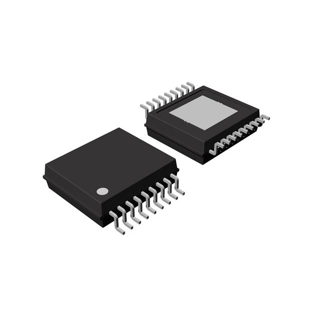
operation is optionally available. The R1272S is available in HSOP-18 package.
FEATURES
● Operating Voltage (Maximum Rating) ······················· 4.0 V to 34 V (36 V)
● Operating Temperature Range ································ -40°C ≤ Ta ≤ 105°C
(Usable in high-temperature environment)
● Start-up Voltage ··················································· 4.5 V
● Output Voltage ················· ··································· 0.7 V to 5.3 V
● Feedback Voltage Tolerance ················· ················· 0.64 V ± 1%
● Consumption Current at No Load (at VFM mode) ········ Typ.15 µA
● Adjustable Oscillation Frequency(1) ········ ·················· 250 kHz to 1 MHz
● Synchronizable Clock Frequency(1)··························· 250 kHz to 1 MHz
● Spreading Rate for SSCG ······································ Typ. ±3.6%
● Minimum On-Time ··· ············································ Typ.100 ns
● Minimum Off-Time ················································ Typ.120 ns (at regulation mode)
At dropout, actual minimum off-time is reduced.
● Adjustable Soft-start Time(2) ···································· Typ.500 µs
● Pre-bias Start-up
● Anti-phase Clock Output
● Thermal Shutdown Function ··································· Tj = 160ºC (Typ.)
(1)
The adjustable oscillation frequency range becomes 250 kHz ≤ fOSC ≤ 600 kHz when 0.7 V ≤ VOUT < 1.35V.
500 µs (Typ.) as a lower limit with using an external capacitor. Otherwise, available the tracking function through the
application of an external voltage.
(2)
1
�R1272S
NO.EA-351-210910
● Under Voltage Lockout (UVLO) Function········· ·········· Typ. 3.3 V
● Over Voltage Detection (OVD) Function ···················· FB pin voltage (VFB) + 10% (Typ.)
Detection/Release Hysteresis ································· FB pin voltage (VFB) x 3% (Typ.)
● Under Voltage Detection (UVD) Function ···················
Detection/Release Hysteresis ·································
● Over-current Protection··········································
● Selectable Current Limit Threshold ···························
● Power Good Output ··············································
● Package ·····························································
FB pin voltage (VFB) - 10% (Typ.)
FB pin voltage (VFB) x 3% (Typ.)
Hiccup-mode / Latch mode
50 mV / 70 mV / 100 mV
NMOS Open-drain Output
HSOP-18
APPLICATIONS
● Power source for digital home appliances such as digital TV, DVD players.
● Power source for office equipment such as printers and fax machines.
● Power source for mobile communication equipment, cameras and video instruments.
● Power source for high voltage battery-powered equipment.
SELECTION GUIDE
The function and setting for the ICs are selectable at the user’s request.
Product Name
Package
Quantity per Reel
Pb Free
Halogen Free
R1272SxxyA-E2-FE
HSOP-18
1,000
Yes
Yes
xx : Select the combination of processing and function.
xx
Over Current Protection
SSCG
00
Non-latch type hiccup mode
Disable
01
Latch mode
Disable
03
Latch mode
Enable
10
Non-latch type hiccup mode
Disable
11
Latch mode
Disable
13
Latch mode
Enable
Output Voltage Range
3.15 V < VOUT ≤ 5.3 V
3.15 V < VOUT ≤ 5.3 V
3.15 V < VOUT ≤ 5.3 V
0.7 V ≤ VOUT ≤ 3.15 V
0.7 V ≤ VOUT ≤ 3.15 V
0.7 V ≤ VOUT ≤ 3.15 V
If required a version with SSCG function, please contact our sales offices.
y : Select the current limit threshold voltage.
y
Set Voltage for Current
Limit Threshold (Typ.)
Reverse Current Detection
Value (Typ.)
1
50 mV
25mV
2
70 mV
35mV
3
100 mV
50mV
2
�R1272S
NO.EA-351-210910
BLOCK DIAGRAMS
VIN
VOUT
Thermal Shutdown
VCC
0.6V
+
UVLO
CE
1.2V
Mode
Select
MODE
OVP
Hiccup
/Latch
EN
VCC Regulator
PFC
Freq
Detection
VCC
VCC
Filter
<Enable/ Disable>
OVD
SHDN
Freq_NG
(BADFREQ)
BST
CLK
Set_Pulse
VCO
RT
HGATE
Mode
AVIN
VOUT
Mode
Rev
Int_Reg
+
SSCG_EN
Mode
INT Regulator
OVP
SHDN
OFF_Pulse
OFF_Pulse
Soft_Start
Drive
Circuit
LX
VFM Control
LGATE
Over Voltage Detection
OVD
Under Voltage Detection
UVD
FB
PGND
Int_Reg
Rev
Set_Pulse
2μA
S
Q
Reverse
Detection
-
Mode
OVD
SHDN
AGND
+
CSS/TRK
+
Soft Start
Circuit
Soft_Start
ILIM
OVD
SHDN
Freq_NG
(BADFREQ)
R
Hiccup
/Latch
Hiccup/Latch
Limit Circuit
OVP
UVD
Peak Limit
Circuit
SENSE
Reference
COMP
VOUT
VCC
PGOOD
Slope
Soft_Start
SHDN
CLK
OVD
UVD
VIN VOUT
CLKOUT
R1272SxxxA
3
�R1272S
NO.EA-351-210910
PIN DESCRIPTIONS
HSOP-18
VCC
18
BST
17
HGATE
16
LX
15
LGATE
14
VOUT
PGND
13
7
RT
MODE
12
8
COMP
PGOOD
11
9
FB
CLKOUT
10
1
VIN
2
CSS
/TRK
3
AGND
4
CE
5
SENSE
6
TOP VIEW
PAD*
HSOP-18 Pin Description
Pin No.
Pin Name
Description
1
VIN
Power supply pin
2
CSS/TRK
3
AGND
4
CE
5
SENSE
6
VOUT
7
RT
8
COMP
9
FB
10
CLKOUT
Clock output pin
11
PGOOD
Power-good output pin
12
MODE
Mode-set input pin
13
PGND
Power GND pin
14
LGATE
L-side FET control pin
15
LX
16
HGATE
17
BST
Boostrap pin
18
VCC
VCC output pin
Soft-start adjustment pin
Analog GND pin
Chip enable pin (Active ”H”)
Sense pin for inductor current
Output voltage feedback input pin
Oscillation adjustment pin
Capacitor connecting pin for phase compensation of error amplifier
Feedback input pin to the error amplifier
Switchingpin
H-side FET control pin
∗ The tab on the bottom of the package must be electrically connected to GND (substrate level) when mounted on the
board.
4
�R1272S
NO.EA-351-210910
INTERNAL EQUIVALENT CIRCUIT FOR EACH PIN
VIN
VIN
Int_Reg
CE
Int_Reg
< VIN Pin >
< CE Pin >
VIN
VIN
VCC
VIN
VOUT
CSS/TRK
1kΩ
Int_Reg
< CSS/TRK Pin >
VIN
< VOUT Pin >
Int_Reg
VCC
Int_Reg
Int_Reg
RT
SENSE
< SENSE Pin >
< RT Pin >
5
�R1272S
NO.EA-351-210910
Int_Reg
COMP
VCC
FB
< COMP Pin >
VCC
< FB Pin >
VCC
PGOOD
CLKOUT
< CLKOUT Pin >
< PGOOD Pin >
VCC
VCC
VCC
VCC
LGATE
MODE
PGND
< MODE Pin >
PGND
PGND
PGND
< LGATE Pin >
6
�R1272S
NO.EA-351-210910
BST
BST
BST
LX
LX
BST
VIN
HGATE
HGATE
LX
LX
< LX Pin >
BST
< BST Pin >
< HGATE Pin >
VCC
< VCC Pin >
AGND
PGND
< AGND-PGND Pins >
7
�R1272S
NO.EA-351-210910
ABSOLUTE MAXIMUM RATINGS
Symbol
VIN
VCE
VCSS/VTRK
VOUT
VSENSE
VRT
VCOMP
VFB
VCC
VBST
VHGATE
VLX
VLGATE
VMODE
VPGOOD
VCLKOUT
PD
Tj
Tstg
Item
VIN pin voltage
CE pin voltage
CSS/TRK pin voltage
VOUTpin voltage
SENSEpin voltage
RT pin voltage
COMP pin voltage( 1)
FB pin voltage
VCC pin voltage
Output current for VCC pin
BST pin voltage
HGATE pin voltage
LX pin voltage(2)
LGATE pin voltage(1)
MODE pin voltage
PGOOD pin voltage
CLKOUT pin voltage(1)
Power Dissipation(3)
(HSOP-18, JEDEC STD.51-7 Test Land Pattern)
Junction Temperature
Storage Temperature Range
Rating
-0.3 to 36
-0.3 to 36
-0.3 to 3
-0.3 to 6
-0.3 to 6
-0.3 to 3
-0.3 to 6
-0.3 to 3
-0.3 to 6
Internally limited
LX-0.3 to LX+6
LX-0.3 to BST
-0.3 to 36
-0.3 to 6
-0.3 to 6
-0.3 to 6
-0.3 to 6
Unit
V
V
V
V
V
V
V
V
V
mA
V
V
V
V
V
V
V
3100
mW
-40 to 125
-55 to 125
°C
°C
ABSOLUTE MAXIMUM RATINGS
Electronic and mechanical stress momentarily exceeded absolute maximum ratings may cause permanent damage
and may degrade the life time and safety for both device and system using the device in the field.
The functional operation at or over these absolute maximum ratings are not assured.
RECOMMENDED OPERATING CONDITIONS
Symbol
VIN
Ta
VOUT
Item
Input Voltage
Operating Temperature Range
Output Voltage Range
Rating
4.0 to 34
−40 to 105
0.7 to 5.3
Unit
V
°C
V
RECOMMENDED OPERATING CONDITIONS
All of electronic equipment should be designed that the mounted semiconductor devices operate within the
recommended operating conditions. The semiconductor devices cannot operate normally over the recommended
operating conditions, even if they are used over such ratings by momentary electronic noise or surge. And the
semiconductor devices may receive serious damage when they continue to operate over the recommended
operating conditions.
(1)
(2)
(3)
The pin voltage must be prevented from exceeding VCC +0.3V.
The pin voltage must be prevented from exceeding VIN +0.3V.
Refer to POWER DISSIPATION for detailed information.
8
�R1272S
NO.EA-351-210910
ELECTRICAL CHARACTERISTICS
VIN = 12 V, CE = VIN, unless otherwise specified.
The specifications surrounded by
are guaranteed by design engineering at -40°C ≤ Ta ≤ 105°C.
R1272SxxxA
(Ta = 25°C)
Symbol
VSTART
VCC
ISTANDBY
IVIN1
IVIN2
VUVLO2
VUVLO1
Item
Conditions
Min.
Typ.
Max.
Unit
4.5
V
5.1
5.3
V
3
20
µA
1.0
1.3
Start-up Voltage
VCC Pin Voltage (VCC–AGND) VFB = 0.672 V
Standby Current
VIN
Consumption
Current 1
at Switching
Stop in PWM
mode
VIN
Consumption
Current 2
at Switching
Stop in VFM
mode
R1272S0xx
R1272S1xx
R1272S0xx
R1272S1xx
UVLO Threshold Voltage
VIN = 34 V, CE = 0 V
VFB = 0.672 V,
MODE = 5 V,
VOUT = SENSE = LX = 5 V
VFB = 0.672 V,
MODE = 5 V,
VOUT = SENSE = 1.5 V,
LX = 5 V
VFB = 0.672 V,
MODE = 0 V
VOUT = SENSE = LX = 5 V
VFB = 0.672V,
MODE = 0 V
VOUT = SENSE = 1.5 V,
LX = 5 V
VCC Rising
4.9
mA
1.6
1.9
15
75
µA
45
145
3.85
4.0
4.2
V
VCC Falling
3.1
3.3
3.4
V
Ta = 25°C
0.6336
-40°C ≤ Ta ≤ 105°C
0.6272
0.64
0.6464
VFB
FB Voltage Accuracy
fOSC0
Oscillation Frequency 0
RT = 135 kΩ
225
250
275
kHz
fOSC1
Oscillation Frequency 1
RT = 32 kΩ
900
1000
1100
kHz
tOFF
Minimum OFF Time
VIN = 5 V, VOUT = 5 V
120
190
ns
tON
Minimum ON Time
100
120
ns
250
fosc×1.5
kHz
fosc×0.5
0.6528
V
fSYNC
Synchronizing Frequency
fOSC as the reference
tSS1
Soft-start Time 1
CSS / TRK = OPEN
0.4
0.75
ms
tSS2
Soft-start Time 2
CSS = 4.7 nF
1.4
2.0
ms
CSS / TRK = 0 V
1.8
2.2
µA
ITSS
VSSEND
RDIS_CSS
RUPHGATE
Charge Current for Soft-start
Pin
CSS/TRK Pin Voltage at End of
Soft-start
Discharge Resistance for
CSS/TRK Pin
On-resistance of Pull-up
Transistor (HGATE Pin)
VFB
VIN = 4.5 V, CE = 0 V,
CSS / TRK = 3 V
(BST – LX) = 5 V,
IHGATE = -100 mA
2.0
1000
2
VFB
VFB+0.06
+0.03
V
3.0
5.0
kΩ
2.5
5.0
Ω
9
�R1272S
NO.EA-351-210910
VIN = 12 V, CE = VIN, unless otherwise specified.
The specifications surrounded by
are guaranteed by design engineering at -40°C ≤ Ta ≤ 105°C.
R1272SxxxA Continued
Symbol
RDOWNHGATE
RUPLGATE
RDOWNLGATE
VILIMIT
VIREVLIMIT
Item
On-resistance of Pull-down
Transistor (HGATE Pin)
On-resistance of Pull-up
Transistor (LGATE Pin)
On-resistance of Pull-down
Transistor (LGATE Pin)
Current Limit Threshold Voltage
(SENSE – VOUT)
Reverse Current Sense
Threshold
(SENSE – VOUT)
(Ta = 25°C)
Conditions
(BST – LX) = 5 V,
IHGATE = 100 mA
(VCC – PGND) = 5 V,
ILGATE = -100 mA
(VCC – PGND) = 5 V,
ILGATE = 100 mA
R1272Sxx1x
Typ.
Max.
Unit
1.5
3.5
Ω
4.0
7.0
Ω
1.5
3.5
Ω
40
50
60
mV
R1272Sxx2x
60
70
80
mV
R1272Sxx3x
90
100
110
mV
-35
-25
-15
mV
-45
-35
-25
mV
-60
-50
-40
mV
0.345
0.43
0.520
V
0.330
0.43
0.515
V
MODE = H/CLK
R1272Sxx1x
MODE = H/CLK
R1272Sxx2x
MODE = H/CLK
R1272Sxx3x
Min.
VCEH
LX Short to GND Detector
Threshold Voltage
(VIN – LX)
LX Short to VCC Detector
Threshold Voltage
(LX – PGND)
CE ”High” Input Voltage
VCEL
CE ”Low” Input Voltage
ICEH
CE ”High” Input Current
CE = 34 V
0.20
ICEL
CE ”Low” Input Current
CE = 0 V
-1.00
IFBH
FB ”High” Input Current
VFB = 3 V
IFBL
FB ”Low” Input Current
VFB = 0 V
VLXSHORTL
VLXSHORTH
1.27
1.14
V
2.45
µA
1.00
µA
-0.10
0.10
µA
-0.10
0.10
µA
VMODEH
MODE ”High” Input Voltage
VMODEL
MODE ”Low” Input Voltage
IMODEH
MODE ”High” Input Current
MODE = 6 V
1.00
IMODEL
MODE ”Low” Input Current
MODE = 0 V
-1.00
VCLKOUTH
VCLKOUTL
TTSD
TTSR
CLKOUT Pin ”High”
Output Voltage
CLKOUT Pin ”Low”
Output Voltage
Thermal Shutdown Threshold
Temperature
V
0
1.33
V
0
0.74
V
6.60
µA
1.00
µA
CLKOUT = Hi-z
4.7
VCC
V
CLKOUT = Hi-z
0
0.1
V
Ta Rising
150
160
°C
Ta Falling
125
140
°C
10
�R1272S
NO.EA-351-210910
VIN = 12 V, CE = VIN, unless otherwise specified.
The specifications surrounded by
are guaranteed by design engineering at -40°C ≤ Ta ≤ 105°C.
R1272SxxxA Continued
(Ta = 25°C)
Symbol
Item
VPGOODOFF
PGOOD “Low” Output Voltage
IPGOODOFF
PGOOD Pin Leakage Current
VFBOVD1
VFBOVD2
VFBUVD1
VFBUVD2
gm (EA)
FB Pin OVD Threshold Voltage
FB Pin UVD Threshold Voltage
Trans Conductance Amplifier
Conditions
VIN = 4.0 V,
PGOOD = 1 mA
VIN = 34 V,
PGOOD = 6 V
VFB Rising
Min.
Typ.
Max.
Unit
0.26
0.54
V
0.10
µA
0.680
VFB×1.10
0.740
V
VFB Falling
0.664
VFB×1.07
0.712
V
VFB Falling
0.556
0.604
V
0.574
VFB×0.90
VFB Rising
0.628
V
0.35
VFB×0.93
COMP = 1.5 V
1
1.55
mS
-0.10
0
All test items listed under Electrical Characteristics are done under the pulse load condition (Tj ≈ Ta = 25°C).
11
�R1272S
NO.EA-351-210910
OPERATING DESCRIPTIONS
MODE Pin Function
The R1272S operating mode is switched among the forced PWM mode, PWM/VFM auto-switching mode and
PLL_PWM mode, by a voltage or a pulse applied to MODE pin. The forced PWM mode is selected when the
voltage of the MODE pin is more than 1.33 V, and the PWM works regardless of a load current. The PWM/VFM
auto-switching mode is selected when it is less than 0.74 V, and control is switched between a PWM mode
and a VFM mode depending on the load current.
See Forced PWM mode and VFM mode for details. And see Frequency Synchronization Function for the
operation on connecting an external clock.
Frequency Synchronization Function
The R1272S can synchronize to the external clock being inputted via the MODE pin, with using a PLL (Phaselocked loop). The forced PWM mode is selected during synchronization. The external clock with a pulse-width
of 100 ns or more is required. The allowable range of oscillation frequency is 0.5 to 1.5 times of the set
frequency(1), and the operating guaranteed frequency is in the 250 kHz to 1 MHz range(2). The R1272S can
synchronize to the external clock even if the soft-start works. That is, the R1272S executes the soft-start and
the synchronization functions at a time if having started up while inputting an external clock to the MODE pin.
When the maxduty or the duty_over state is caused by reduction in differential between input and output
voltages, the device runs at asynchronous to the MODE pin, and it operates in the frequency reduced until
one-fourth of the external clock frequency. Likewise, the CLKOUT pin becomes asynchronous to the MODE
pin. If making synchronization to the MODE pin, take notice in use under a reduced input voltage.
Duty_over Function
When the input voltage is reduced at cranking, the operating frequency is reduced until one-fourth of the set
frequency with being linearly proportional to time in order to maintain the output voltage. Exploiting the ON
duty to exceed the maxduty value at normal operation can make the differential between input and output
voltages small.
PGOOD (Power Good) Output Function
The power good function with using a NMOS open drain output pin can detect the following states of the
R1272S. The NMOS turns on and the PGOOD pin becomes “Low” when detecting them. After the R1272S
returns to their original state, the NMOS turns off and the PGOOD pin outputs “High” (PGOOD Input Voltage:
VUP).
・CE = “L” (Shut down)
・UVLO (Shut down)
・Thermal Shutdown
・Soft-start time
(1)
(2)
See Oscillation Frequency Setting for details of the set frequency.
The adjustable oscillation frequency range becomes 250 kHz ≤ fOSC ≤ 600 kHz when 0.7 V ≤ VOUT < 1.35V.
12
�R1272S
NO.EA-351-210910
・at UVD Threshold Voltage Detection
・at OVD Threshold Voltage Detection
・at hiccup-type Protection (when hiccup mode is selected)
・at latch-type Protection (when latch mode is selected)
The PGOOD pin is designed to become 0.54 V or less in “Low” level when the current floating to the PGOOD
pin is 1 mA. The use of the PGOOD input voltage (VUP) of 5.5 V or less and the pull-up resistor (RPG) of 10
kΩ to 100 kΩ are recommended. If not using the PGOOD pin, connect it to “Open” or “GND”.
R1272S
PGOOD
RPG
VUP
VPGOOD
“H” is detected under
abnormal condition.
PGOOD Output Pin Connecting Diagram
VIN
1.1V
time
CE
time
VFB
0.64V
time
PGOOD
Hi-z
120us
(Typ.)
Hi-z
time
Rising / Falling Sequence of Power Good Circuit
13
�R1272S
NO.EA-351-210910
Under Voltage Detection (UVD)
The UVD function indirectly monitors the output voltage with using the FB pin.
The PGOOD pin outputs “L”
when the UVD detector threshold is 90% (Typ.) of VFB and VFB is less than the UVD detector threshold for
more than 30 µs (Typ.). When VFB is over 93% (Typ.) of 0.64 V, the PGOOD pin outputs “H” after delay time
(Typ.120 µs.). And, the hiccup- / latch-type overcurrent protection works when detecting an overcurrent, an LX
power supply protection, or an over voltage protection during the UVD detection.
Over Voltage Detection (OVD)
The OVD function indirectly monitors the output voltage with using the FB pin. Switching stops even if the
internal circuit is active state, when detecting the over voltage of VFB. The PGOOD pin outputs “L” when the
OVD detector threshold is 110% (Typ.) of VFB and VFB is over the OVD detector threshold for more than 30 µs
(Typ.). When VFB is under 107% (Typ.) of VFB, which is the OVD released voltage, the PGOOD pin outputs “H”
after delay time (Typ.120 µs.). Then, switching is controlled by normal operation. The over voltage protection
works when an error is caused by a feedback resistor in peripheral circuits for the FB pin.
Over Voltage Protection (OVP)
The OVP function monitors the voltage of VOUT pin to reduce an over voltage, when an error is caused in
peripheral circuits for the FB pin. Switching stops even if the internal circuit is active state, when VOUT is over
the OVP detector threshold. When VOUT is under the OVP detector threshold, switching is controlled by normal
operation. If the UVD for FB pin occur during the OVP detect state, an error will occur and hiccup- / latch-type
protection will work. However, the operation under this function is not guaranteed because the OVP detector
threshold is set to the absolute maximum rating and more for the VOUT pin.
LX Power Supply (VIN Short) / GND (GND Short) Protection
In addition to normal current limit, the R1272S provides the LX power supply / GND short protection to monitor
the voltage between the FET’s drain and source. Since the current limit function is controlled with an external
inductor’s DCR or a sense resistance, the current limit function cannot work when a through-current is flowed
through the FET and when an overcurrent is generated by shorting the LX pin to VDD/GND. The detecting
current is determined by LX shot to VDD/GND detector threshold voltage (FET_On-resistance x Current,
Typ.0.43 V).
Hiccup-type / Latch-type Overcurrent Protection
The hiccup-type / latch-type overcurrent protection can work under the operating conditions that is the UVD
can function during the current limit or OVP and the LX GND short protection. The latch-type protection can
release the circuit by setting the CE pin to “L” or by reducing VIN to be less than the UVLO detector threshold,
when the output is latched off.
The hiccup type protection stops switching releases the circuit after the
protection delay time (Typ. 3.5 ms). Since this protection is auto-release, the CE pin switching of “L” / “H” is
unnecessary. And, damage due to the overheating might not be caused because the term to release is long.
When the output is shorted to GND, switching of “ON” / “OFF” is repeated until the shorting is released.
14
�R1272S
NO.EA-351-210910
Current Limit Function
The current limit function can be to limit the current by the peak current method to turn the high-side FET off
that the potential differences is over the current limit threshold voltage. The threshold voltage is selectable
among 50 mV / 70 mV / 100 mV. And, the two following detection methods can be selected by external
components connected.
A. Detecting Method with RSENSE
The current limit value is detected with the voltage across the inductor that a sense resistance is connected in
series. By connecting a resistance with low level of variation, the current limit with high accuracy can achieve.
As a result, be caution that the power loss is caused from the current and RSENSE. The peak current in the
current limit inductor can be calculated by the following equation.
Peak current in Current limit inductor (A) = Current limit threshold voltage (mV) / RSENSE (mΩ)
H-side
FET
SENSE
VOUT
LX
L-side
FET
COUT
RSENSE
Inductor
Figure A Detection with Sense Resistance
B. Detecting Method with DCR of Inductor
The current limit value is detected with the DCR of the inductor. The reduction of the loss is minimized since
the inductor is in no need of a resistance. But, the SENSE pin requires to connect a resistor and a capacitor
to each end of the inductor. Because a constant slope is caused depending on the inductance and the
capacitance. Factors causing the poor accuracy of current limit value include the variation in production of the
inductor’s DCR and the temperature characteristics. RS and CS can be calculated by the following equation.
Peak current in Current limit inductor (A) = Current limit threshold voltage (mV) / Inductor’s DCR (mΩ)
CS = L / (DCR x RS)
SENSE
RS
CS
H-side
FET
VOUT
LX
L-side
FET
Figure B
Inductor
DCR
COUT
Detecting with Inductor’s DCR
15
�R1272S
NO.EA-351-210910
Output Voltage Setting
The output voltage (VOUT) can be set by adjustable values of RTOP and RBOT. The value of VOUT can be
calculated by Equation 1 :
VOUT = VFB × (RTOP + RBOT) / RBOT ············································································· Equation1
For example, when setting VOUT = 3.3 V and setting RBOT = 22 kΩ, RTOP can be calculated by substituting them
to Equation 1. As a result of the expanding Equation 2, RTOP can be set to 91.4 kΩ.
To make 91.4 kΩ with using the E24 type resistors, the connecting use of 91 kΩ and 0.39 kΩ resistors in series
is required. If the tolerance level of the set output voltage is wide, using a resistor of 91 kΩ to RTOP can reduce
the number of components.
RTOP = (3.3 V / 0.64 V - 1) × 22 kΩ
= 91.4 kΩ ···································································································· Equation2
As to R1272S00x, R1272S01x and R1272S03x, RTOP and RBOT should be selected to meet the required output
voltage (VOUT) > 2.91 V with a variation in resistance taken into account.
Oscillation Frequency Setting
Connecting the oscillation frequency setting resistor (RRT) between the RT pin and GND can control the
oscillation frequency in the range of 250 kHz to 1 MHz(1). For example, using the resistor of 66 kΩ can set the
frequency of about 500 kHz.
The Electrical Characteristics guarantees the oscillation frequency under the conditions stated below for fOSC0
(at RRT = 135 kΩ) and fOSC1 (at RRT = 32 kΩ).
(1)
The adjustable oscillation frequency range becomes 250 kHz ≤ fOSC ≤ 600 kHz when 0.7 V ≤ VOUT < 1.35V.
16
�R1272S
NO.EA-351-210910
1200
1000
fosc [kHz]
800
600
400
200
0
30
50
70
90
RRT [kΩ]
110
130
150
RRT [kΩ] = 41993 x fOSC [kHz] ^ (-1.039)
R1272S001A Oscillation Frequency Setting Resistor (RRT) vs. Oscillation Frequency (fOSC)
Soft-start Function
The soft-start time is a time between a rising edge (“H” level) of the CE pin and the timing when the output
voltage reaches the set output voltage. Connecting a capacitor (CSS) to the CSS / TRK pin can adjust the softstart time (tSS) – provided the internal soft-start time of 500 µs (Typ.) as a lower limit. The adjustable soft-start
time (tSS2) is 1.6 ms (Typ.) when connecting an external capacitor of 4.7 nF with the charging current of 2.0
μA (Typ.). If not required to adjust the soft-start time, set the CSS / TRK pin to “Open” to enable the internal
soft-start time (tSS1) of 500 µs (Typ.). If connecting a large capacitor to an output signal, the overcurrent
protection or the LX GND short protection might run. To avoid these protections caused by starting abruptly
when reducing the amount of power current, soft-start time must be set as long as possible.
Each of soft-start time (tss1/ tss2) is guaranteed under the conditions described in the chapter of “Electrical
Characteristics”.
17
�R1272S
NO.EA-351-210910
tSS
10ms
3.3ms
CSS [nF] = (tSS - tVO_S) / 0.64 × 2.0
1.6ms
tSS: Soft-start time (ms)
1.2ms
tVO_S: Time period from CE = “H” to VOUT’s rising
(Typ. 0.160 ms)
0.5ms
CSS
1nF
3.3nF 4.7nF 10nF
33nF
Soft-start Time Adjustable Capacitor (CSS) vs. Soft-start Time (tSS)
tSS
CE
tVO_S
1.27V
time
VOUT
VSET
time
PGOOD
120us
(Typ.)
time
Soft-start Sequence
Tracking Function
Applying an external tracking voltage to the CSS / TRK pin can control the soft-start sequence – provided that
the lowest internal soft-start time is limited to 500 µs (Typ.). Since VFB becomes nearly equal to VCSS/TRK at
tracking, the complex start timing and soft-start can be easily designed. The available voltage at tracking is
between 0 V and 0.64 V. If the tracking voltage is over 0.64 V, the internal reference voltage of 0.64 V is
enabled. Also, an arbitrary falling waveform can be generated by reducing VCSS/TRK to 0.64 V (Typ.) or less,
because the R1272S supports both of up- and down- tracking.
18
�R1272S
NO.EA-351-210910
VOUT
0.64V
CSS/TRK
SS
Normal Operation
SS
Tracking Sequence
Min. ON-time
The min. ON time (Max. 120 ns), which is determined in the R1272S internal circuit, is a minimum time to turn
high-side FET on. The R1272S cannot generate a pulse width less than the min. ON time. Therefore, settings
of the output set voltage and the oscillator frequency are required so that the minimum step-down ratio
[VOUT/VIN x (1 / fOSC)] does not stay below 120ns. If staying below 120 ns, the pulse skipping will operate to
stabilize the output voltage. However, the ripple current and the output voltage ripple will be larger.
Min. OFF-time
By the adoption of bootstrap method, the high-side FET, which is used as the R1272S internal circuit for the
min. OFF time, is used a NMOS. The voltage sufficient to drive the high-side FET must be charged. Therefore,
the min. OFF time is determined from the required time to charge the voltage. By the adoption of the
frequency’s reduction method by one-quarter of a set value (Min.), if the input-output difference voltage
becomes small or load transients are caused, the OFF period can be caused once in four-cycle period of
normal cycle. As a result, the min. OFF time becomes 30 ns (Typ.) substantially, and the maximum duty cycle
can be improved.
19
�R1272S
NO.EA-351-210910
Through-current Protection
The HGATE pin voltage (VHGATE) and the LGATE pin voltage (VLGATE) are monitored to protect a through-type
current caused by an external FET. In the case of turning-on the low-side FET, after a difference between
VHGATE - LX pin voltage (VLX) becomes 1V or less, increasing VLGATE can prevent not to turn on both of the highside and low-side FETs at a time and thereby prevent the through-current. In the case of turning-on the highside FET, after a difference between VLGATE - GND (PGND pin voltage) becomes 1 V or less, increasing a
difference between VHGATE - VLX can prevent the through-current.
Reverse Current Limit Function
The reverse current limit function works when the output voltage is pulled up more than the set output voltage
by shorting. When the current is over the threshold current to detect the reverse current, the LGATE pin
becomes to “L” to control the reverse current. As with the current limit value, the reverse current limit value is
determined by the voltage between the VOUT pin and the SENSE pin. The detector threshold is one half of
the current limit value.
SSCG (Spread Spectrum Clock Generator)
The SSCG function works for EMI reduction at the PWM mode. This function is enabled in the
R1272S03xA/13xA.
This function makes EMI waveforms decrease in amplitude to generate a ramp waveform within approximately
±3.6% (Typ.) of the oscillator frequency (fOSC). The modulation cycle is fOSC / 128. At the VFM mode, the SSCG
is disabled.
Bad Frequency (BADFREQ) Protection
If a current equivalent to 2 MHz (Typ.) or more or 125 kHz (Typ.) or less is applied to the RT pin when the
resistor of the RT pin is in open / short, the R1272S will stop switching to protect the IC and will cause the
internal state to transition to its state before the soft-start. The CLKOUT pin is fixed to “L” while the bad
frequency as above is detected. The R1272S will restart under the normal control from the state of soft-start
when recover after the abnormal condition.
VFB
BADFEQ
Detection
BADFEQ
Release
0.64V
CLKOUT
time
PGOOD
time
time
BADFREQ Detection / Release Sequence
20
�R1272S
NO.EA-351-210910
Operation of Step-down Converter
A basic step-down DC/DC converter circuit is illustrated in the following figures. This DC/DC converter charges
energy in the inductor when the high-side FET turns on, and discharges the energy from the inductor when
the high-side FET turns off and controls with less energy loss, so that a lower output voltage than the input
voltage is obtained.
IL
i1
H-side FET
VIN
VOUT
L
L-side FET
i2
ILMIN
tOPEN
COUT
tON
GND
tOFF
t=1/ fOSC
Basic Circuit
Step1.
ILMAX
Current Through Inductor
The high-side FET turns on and current IL (= i1) flows, and energy is charged into COUT. At this
moment, IL increases from ILMIN (= 0) to reach ILMAX in proportion to the on-time period (ton) of the
high-side FET turns on and current IL (= i1) flows, and energy is charged into COUT. At this moment,
IL increases from ILMIN (= 0) to reach ILMAX in proportion to the on-time period (tON) of the high-side
FET.
Step2.
When the high-side FET turns off, the low-side FET turns on in order to maintain IL at ILMAX, and
current IL (= i2) flows.
Step3.
When MODE = L (VFM/PWM Auto-switching mode),
IL (= i2) decreases gradually and reaches IL = ILMIN = 0 after a time period of tOPEN, and the low-side
FET turns off. This case is called as discontinuous mode. The VFM mode is switched if go to the
discontinuous mode. If the output current is increased, a time period of tOFF runs out prior to reach of
IL = ILMIN = 0. The result is that the high-side FET turns on and the low-side FET turns off in the next
cycle. This case is called continuous mode.
When MODE = H (Forced PWM mode), MODE = External Clock (PLL_PWM mode),
Since the continuous mode works at all time, the low-side FET turns on until going to the next cycle.
That is, the low-side FET must keep “On” to meet IL = ILMIN < 0, when reaches IL = ILMIN = 0 after a
time period of tOPEN.
In the PWM mode, the output voltage is maintained constant by controlling tON with the constant switching
frequency (fOSC).
21
�R1272S
NO.EA-351-210910
Forced PWM Mode and VFM Mode
The output voltage control methods are selectable between the PWM / VFM Auto-switching mode and the
forced PWM mode by using the MODE pin.
Forced PWM Mode
Forced PWM mode is selected when setting the MODE pin to “H”. This mode can reduce the output noise,
since the frequency is fixed during light load conditions. Thus, ILMIN becomes less than "0" when IOUT is less
than ∆IL/2.
That is, the electric charge, which is charged to COUT, is discharged via FET for the durations –
when IL reaches “0” from ILMIN during the tON periods and when IL reaches ILMIN from “0” during tOFF periods.
But, pulses are skipped to prevent the overvoltage when high-side FET is set to ON under the condition that
the output voltage being more than the set output voltage.
VFM Mode
PWM / VFM Auto-switching mode is selected when setting the MODE pin to “L”. This mode can automatically
switch from PWM to VFM to achieve a high-efficiency during light load conditions. By the VFM mode
architecture, the high-side FET is turned on for tON x 1.54 (typ.) at the PWM mode under the same condition
as the VFM mode when the VFB pin voltage drops below the internal reference voltage (Typ.0.64 V). After the
On-time, the high-side FET is turned off and the low-side FET is turned on. When the inductor current of 0 A is
detected, the low-side FET is turned off and the switching operation is stopped (Both of hi- and low-side FETs
are OFF). The switching operation restarts when the VFB pin voltage becomes less than 0.64 V.
The On-time at the PWM mode is determined by a resistance, input and output voltages, which are connected
to the RT pin. Refer to “Calculation of VFM Ripple” for detailed description on the On-time at the VFM mode.
ILMAX
IL
ILMAX
IL
ΔIL
IOUT
0
0
ILMIN
tON
t
tOFF
T=1/fOSC
Forced PWM Mode
ILMIN
t
tON
tOFF
VFM Mode
22
�R1272S
NO.EA-351-210910
Calculation of VFM Ripple
Calculation example of output ripple voltage (VOUT_VFM) is described. VOUT_VFM can be calculated by Equation
1. And, the maximum value of inductor current (IL_VFM) can be calculated by Equation 2.
VOUT_VFM = RCOUT_ESR × (IL_VFM) + COEF_TON_VFM × (IL_VFM / 2) / fOSC / COUT_EFF ························· Equation1
IL_VFM = ((VIN -VOUT) / L) × COEF_TON_VFM × VOUT / VIN / fOSC ··············································· Equation 2
VOUT_VFM : Output ripple
RCOUT_ESR : ESR of output capacitor
IL_VFM : Maximum current of inductor
COEF_TON_VFM : Scaling factor of On-time - Typ.1.54X (Design value)
(VIN-VOUT) / L : Slope of inductor current
COEF_TON_VFM × VOUT / VIN / fOSC : On-time
IL (A)
Inductor Current (Max.)
IL_VFM
Slope
Slope
⊿IL=(VIN-VOUT)/L
⊿IL= VOUT/L
Average Area of
IL (A) x Time (s)
T1
T2
Time(s)
H-side FET
L-side FET
Inductor Current Waveform at VFM Mode
23
�R1272S
NO.EA-351-210910
Output voltage can be calculated by the following simple equation.
VOUT = I × T/C
I : Current, C : Capacitance, T : Time
Since I is represented by 1/2 x IL_VFM as the average current, the time of current passing at the VFM mode can
be expressed by the following equation.
T = COEF_TON_VFM / fOSC
And, the output ripple voltage (VOUT_VFM) is superimposed a voltage for ESR × I, and Equation 1 is determined.
But, ESR is so small that it may be ignored if ceramic capacitors are connected in parallel.
The amount of charge to the output capacitor can be calculated by Equation 3.
(High-side FET On-time (T1) + Low-side FET On-time (T2)) × Average amount of current
··············· Equation3
Then, T1 and T2 can be calculated by the following equations, and the time of current passing can be
determined.
T1 = COEF_TON_VFM / fOSC × VOUT / VIN ····· (On-time at VFM)
T2 = (VIN/VOUT-1) × T1 (0 = IL_VFM – VOUT/L × T2)
T = T1 + T2
= VIN /VOUT × T1
= COEF_TON_VFM / fOSC
And then, the amount of charge can be determined as Equation 4.
T x IL_VFM /2 = COEF_TON_VFM / fOSC × IL_VFM /2 ······························································· Equation 4
With using above-equations, the output ripple voltage (VOUT_VFM) can be calculated by Equation 5.
V = IT/C = COEF_TON_VFM / fOSC × IL_VFM / 2 / COUT_EFF ···················································· Equation 5
24
�R1272S
NO.EA-351-210910
APPLICATION INFORMAITON
Typical Application Circuit
2.2μF
V CC
V IN
CSS /T RC
B ST
A GND
HGA TE
CE
LX
S ENS E
91.4kΩ
13kΩ
3.3nF
2700pF 47pF
R1272SxxxA
0.22μF
40μF
VIN
4.5V to 34V
2.2μH
LGA TE
V OUT
P GND
RT
MO DE
COMP
P GOOD
V FB
CLKO UT
HS/LS-FET
NP35N04YLG
VOUT
3.3V
6.8mΩ
150μF
1kΩ
24pF
22kΩ
66kΩ
R1272SxxxA Typical Application Circuit at 500 kHz
2.2μF
V CC
V IN
CSS /T RC
B ST
A GND
HGA TE
CE
LX
S ENS E
V OUT
24.3kΩ
5.5kΩ
3.3nF
3.3nF 100pF
R1272SxxxA
LGA TE
0.22μF
20μF
VIN
4.5V to 12V
1.0μH
VOUT
1.35V
5mΩ
200μF
P GND
RT
MO DE
COMP
P GOOD
V FB
CLKO UT
HS/LS-FET
NVTFS5811NLTAG
1kΩ
47pF
22kΩ
33kΩ
R1272SxxxA Typical Application Circuit at 1MHz
25
�R1272S
NO.EA-351-210910
Selection of External Components
External components and its value required for R1272S are described. Each value is reference value at initial.
Since inductor’s variations and output capacitor’s effective value may lead a drift of phase characteristics,
adjustment to a unity-gain and phase characteristics may be required by evaluation on the actual unit.
1.
Determination of Requirements
Determine the frequency, the output capacitor, and the input voltage required. For reference values,
parameters listed in the following table will be used to explain each equation.
Parameter
Output Voltage (VOUT)
Output Current (IOUT)
Input Voltage (VIN)
Input Voltage Range
Frequency (fOSC)
ESR of Output Capacitor (RCOUT_ESR)
2.
Value
3.3 V
10 A
12 V
8 V to 16 V
500 kHz
3 mΩ
Selection of Unity-gain frequency (fUNITY)
The unity-gain frequency (fUNITY) is determined by the frequency that the loop gain becomes “1” (zero dB). It is
recommended to select within the range of one-sixth to one-tenth of the oscillator frequency (fOSC). Since the
fUNITY determines the transient response, the higher the fUNITY, the faster response is achieved, but the phase
margin will be tight. Therefore, it is required that the fUNITY can secure the adequate stability. As for the reference,
the fUNITY is set to 70 kHz.
3.
Selection of Inductor
After the input and the output voltages are determined, a ripple current (∆IL) for the inductor current is
determined by an inductance (L) and an oscillator frequency (fOSC). The ripple current (∆IL) can be calculated
by Equation 1.
∆IL= (VOUT / L / fOSC) x (1-VOUT / VIN_MAX) ········································································· Equation 1
VIN_MAX : Maximum input voltage
The core loss in the inductor and the ripple current of the output voltage become small when the ripple current
(∆IL) is small. But, a large inductance is required as shown by Equation 1. The inductance can be calculated
by Equation 2 when a reference value of ∆IL assumes 30% of IOUT is appropriate value.
L = (VOUT / ∆IL / fOSC) x (1-VOUT / VIN_MAX)········································································· Equation 2
= (VOUT / (IOUT x 0.3) / fOSC) x (1-VOUT / VIN_MAX)
26
�R1272S
NO.EA-351-210910
The inductance can be calculated by substituting each parameter to Equation 2.
L = (3.3 V / 3 A / 500 kHz) x (1-3.3 V / 16 V)
= 1.75 µH
When selecting the inductor of 2.2µH as an approximate value of the above calculated value, ∆IL can be shown
as below.
∆IL = (3.3 V / 2.2 µH / 500 kHz) x (1-3.3 V / 16 V)
= 2.38 A
4.
Setting of Output Capacitance
The output capacitance (COUT) must be set to meet the following conditions.
■ Calculation based on phase margin
To secure the adequate stability, it is recommended that the pole frequency (fP_OUT) is set to become equal or
below one-fourteenth of the unity-gain frequency. The pole frequency (fP_OUT) can be calculated by Equation 3.
fP_OUT = 1/(2 x π x COUT_EFF x ((ROUT_MIN x 2 x π x fOSC x L) / (ROUT_MIN + 2 x π x fOSC x L) + RCOUT_ESR))
················ Equation 3
COUT_EFF : Output capacitance (effective value)
ROUT_MIN : Output resistance at maximum output current
ROUT_MIN = VOUT/ IOUT
= 3.3 V / 10 A
= 0.33 Ω
Equation 4 can be expressed by substituting fP_OUT = fUNITY / 14 to Equation 3.
COUT_EFF = 14 / (2 ×π× fUNITY × ((ROUT_MIN × 2 ×π× fOSC × L) / (ROUT_MIN + 2 ×π× fOSC × L) + RCOUT_ESR))
··············· Equation 4
Then, the output capacitance (effective value) can be calculated by substituting each parameter to Equation
4.
COUT_EFF =14 / (2 ×π×70kHz×((0.33Ω × 2 ×π× 500 kHz × 2.2 µH) / (0.33Ω+ 2 ×π× 500kHz × 2.2µH)+3mΩ))
= 100.1 µF
It is recommended that the output capacitance is set to become equal or over the effective value calculated by
Equation 4.
27
�R1272S
NO.EA-351-210910
The output capacitance (effective value), which is derated depending on the DC voltage applied, can be
calculated by Equation 5. Refer to “Capacitor Manufacture’s Datasheet” for details about derating.
COUT_EFF = COUT_SET × (VCO_AB - VOUT) / VCO_AB ································································· Equation 5
COUT_SET : Output capacitor’s spec
VCO_AB : Capacitor’s voltage rating
With using Equation 5, the effective value is calculated to become 100.1 µF or more. The output voltage
(COUT) can be shown as below when VCO_AB is 10 V.
COUT_SET > COUT_EFF / ((VCO_AB - VOUT) / VCO_AB)
COUT_SET > 100.1µF / ((10 - 3.3) / 10)
COUT > 149.4 µF
As the calculated result, COUT selects a capacitor of 150 µF (the effective value is 100.5 µF).
■ Calculation based on ripple at VFM mode
With using the calculated value of COUT, the amount of ripple at the VFM mode can be shown as Equations 6
and Equation 7.
IL_VFM = ((VIN_MAX-VOUT) / L) × COEF_TON_VFM × VOUT / VIN_MAX / fOSC ········································· Equation 6
VOUT_VFM = RCOUT_ESR × (IL_VFM) + COEF_TON_VFM × (IL_VFM / 2) / fOSC / COUT_EFF ··························· Equation 7
IL_VFM : Maximum current of inductor
COEF_TON_VFM : On-time scaling (multiples of PWM_ON time)
VOUT_VFM : Maximum output ripple
COEF_TON_VFM can be calculated by 1.54 times (Typ.) as the design value. The ripple value can be calculated by
substituting each parameter to Equations 6 and Equation 7.
IL_VFM = ((16 V - 3.3 V ) / 2.2 µH) × 1.54 × 3.3 V / 16 V / 500 kHz
= 3.67 A
VOUT_VFM = 3 mΩ ×3.67 A + 1.54 × (3.67 A / 2) / 500 kHz / 100.5 µF
= 67.2 mV
VOUT_VFM must be set to become the target ripple value or less. If VOUT_VFM is over the target value, the output
capacitance must be calculated by Equation 8.
COUT_EFF = 1.54 × (IL_VFM / 2) / fOSC / (VOUT_VFM - RCOUT_ESR × (IL_VFM)) ····································· Equation 8
28
�R1272S
NO.EA-351-210910
5.
Designation of Phase Compensation
Since the current amplifier for the voltage feedback is output via the COMP pin, the phase compensation is
achieved with using external components. The phase compensation is able to secure stable operation with
using an external ceramic capacitor and the phase compensation circuit.
VOUT
CSPD
RTOP
VFB
ERROR_AMP
COMP
+
RBOT
VREF
0.64V
RC
CC
CC2
Connection Example for External Phase Compensation Circuit
■ Calculation of RC
The phase compensation resistance (RC) to set the calculated unity-gain frequency can be calculated by
Equation 9.
RC = 2 ×π× fUNITY × VOUT × COUT_EFF / (gm_ea × VREF × gm_pwr) ·············································· Equation 9
gm_ea : Error amplifier of gm
VREF : Reference voltage (0.64 V)
gm_pwr : power level of gm
gm_pwr × ∆VS = ∆IL
gm_ea / ∆VS = 0.05 × 10 ^ (-6) × fOSC / VOUT
gm_ea × gm_pwr = 0.05 × 10 ^ (-6) ×∆IL × fOSC / VOUT ························································· Equation 10
∆VS : Output amplitude of the slope circuit
RC can be calculated by substituting Equation 10 to Equation 9.
RC = 2 ×π× fUNITY × VOUT × COUT_EFF / (VREF × 0.05 × 10 ^ (-6) × ∆IL × fOSC / VOUT)
= 2 ×π× 70 kHz × 3.3 V × 100.5 µF / (0.64 × 0.05 × 10 ^ (-6) × 2.38A × 500 kHz / 3.3 V)
=12.63 ≒13 kΩ
29
�R1272S
NO.EA-351-210910
■ Calculation of CC
CC must be calculated by Equation 11 so that the zero frequency of the error amplifier meets the highest pole
frequency (fP_OUT). Then, fP_OUT = 5.0 kHz is determined by calculation of Equation 3.
CC = 1 / (2 ×π× RC × fP_OUT) ····················································································· Equation 11
= 1/ (2 × 3.14 ×13 kΩ × 5.0 kHz)
= 2.45 ≒ 2.7 nF
■ Calculation of CC2
CC2 can be calculated by two different calculation methods to vary from the zero frequency (fZ_ESR) depending
on the ESR of a capacitor.
fZ_ESR can be calculated by Equation 12.
fZ_ESR = 1 / (2 ×π× RCOUT_ESR × COUT_EFF) ···································································· Equation 12
= 528 kHz
[When the zero frequency is lower than fOSC / 2]
CC2 sets the pole to fZ_ESR.
CC2 = RCOUT_ESR × COUT_EFF / RC ·················································································· Equation 13
[When the zero frequency is higher fOSC / 2]
CC2 sets the pole to fOSC / 2 so as to be a noise filter for the COMP pin.
fOSC / 2 = 1 / (2 ×π× RC × CC2)
CC2 = 2 / (2 ×π× RC × fOSC) ······················································································· Equation 14
In the reference example, CC2 is used as the noise filter for the COMP pin because of being higher than fOSC/2.
CC2 = 49 ≒ 47 pF
■ Calculation of CSPD
CSPD sets the zero frequency to meet the unity-gain frequency.
RTOP = RBOT × (VOUT / VREF -1)
CSPD = 1 / (2 ×π× fUNITY × RTOP) ················································································· Equation 15
When RBOT = 22 kΩ,
RTOP = 22 k × (3.3 V / 0.64 V -1)
= 91.4 kΩ
CSPD = 1 / (2 ×π× 70 kHz × 91.4 kΩ)
= 24.8 ≒ 27 pF
30
�R1272S
NO.EA-351-210910
Cautions in Selecting External Components
Inductor
● Choose an inductor that has small DC resistance, has sufficient allowable current and is hard to cause
magnetic saturation. The inductance value must be determined with consideration of load current under the
actual condition. If the inductance value of an inductor is extremely small, the peak current of LX may
increase along with the load current. As a result, the current limit circuit may start to operate when the peak
current of LX reaches to “LX limit current”.
Capacitor
● Choose a capacitor that has a sufficient margin to the drive voltage ratings with consideration of the DC
bias characteristics and the temperature characteristics.
● The use of a ceramic capacitor for CIN is recommended. If combined use of a ceramic and an electrolyte
capacitors, the stable operation will improve since the margin becomes bigger. Choose the electrolyte
capacitor with the lowest possible ESR with consideration of the allowable ripple current rating (IRMS). IRMS
can be calculated by the following equation.
IRMS ≒ IOUT/ VIN x √{ VOUT x (VIN – VOUT) }
FET
● Gate – Source Voltage
When considering variations in production and margin, a FET with a withstand voltage of 10 V or more is
recommended despite the 5 V high and low driver.
● Gate Threshold Voltage
Choose a FET with the threshold voltage between 1.0 V (Min.) and 3.4 V (Max.) with consideration of
variations in production and margin.
● Drain Current
Choose a FET having a sufficient margin with consideration of peak current and limit current.
● Connection of Body Diode for Source Current
Choose a diode with the withstand current over the reverse limit current rating. The R1272S reverse current
value becomes one-half of the normal limit current value.
● Input Capacitor (CISS)
As an index of performance, CISS: 3800pF
● On-resistance (RDS (on)) & All Gate Capacitance (Qg)
Choose a FET with the lowest possible characteristics because having an influence on efficiency. Generally,
a high-performance FET is rated that RDS x Qq (performance figure) is small.
● Since test specifications vary with FET makers, it is necessary to confirm the application with the R1272S
implemented on a board system.
31
�R1272S
NO.EA-351-210910
FET Losses
The FET total loss is calculated by the sum of the switching losses when the high side and the low side FETs
turning-on / off and the conduction losses by the FET’s on-resistance. If the total loss become larger than
expected, the external FET must be selected with consideration of the on-resistance, the switching losses and
the package’s power dissipation. The following figure shows the timing chart of the high side / low side FETs
at normal switching. The loss at each delay time can be calculated as follows.
VCC
HS-FET
VGS
VTH
VSP
VIN
LX
LS-FET VDS
(RONL × IOUT )
VF (Body Diode)
VCC
LS-FET
VGS
VTH
VSP
time
t6
t1
t2
t3
t4
t5
t6
DC / DC Converter Basic Switching Timing Chart
t1 (t5):
For the duration between the low side FET’s turn-off and the high side FET’s turn-on, the loss occurs to
supply a current from the body diode on the low side FET. Likewise, for the duration between the high side
FET’s turn-off and the low side FET’s turn-on, the loss occurs. The losses (PDEAD) for t1 and t5 can be
calculated by the following equation.
PDEAD = VF × IOUT × fOSC × (tDEAD1 + tDEAD5)
VF: The forward voltage of a body-diode
tDEAD1: The delay time from the instant when the gate-source voltage (VGS) falls below the threshold voltage
(VTH) on the low side FET to the instant when VGS exceeds VTH on the high side FET.
TDEAD5: The delay time from the instant when VGS falls below VTH on the high side FET to the instant when
VGS exceeds VTH on the low side FET.
32
�R1272S
NO.EA-351-210910
t2 (t4):
Since the drain-source voltage (VDS) is equal to VIN when the high side FET turns on/off after delay time
(tDEAD1 / tDEAD5), the source current and the output current (IOUT) become equal. Therefore, a large loss
occurs. The losses (PSW) at turn-on / off can be calculated by the following equation.
PSW = 1/2 × VIN × IOUT × fOSC × (tRISE + tFALL)
tRISE: A duration between the gate voltage rising start time from the threshold voltage and the end of
stabilized voltage (VSP) on the high side FET.
TFALL: A duration between the start time of the gate voltage stabilizing and the falling time below the
threshold voltage on the high side FET.
For the stabilized duration, VGS of the high side FET remains constant roughly since the gate charge current
is used to charge CGD. And, the reverse recovery loss (PRR) occurs to recover the body diode of the low
side FET when the high side FET turns on. Refer to the FET datasheet for information about the electric
charge (Qrr) required for recovery.
PRR = VIN × Qrr × fOSC
And, the power (PGH, PGL) for electric charge of the FET’ gate and the power (POSSH, POSSL) for electric
charge of the FET’s output capacity occur. Each power can be calculated by following equations. Refer to
the FET datasheet for detailed values.
PGH = QGH × VCC × fOSC
PGL = QGL × VCC × fOSC
POSSH = 1/2 × COSSH × (VIN)2 × fOSC
POSSL = 1/2 × COSSL × (VIN)2 × fOSC
VCC: VCC pin voltage
QGH, QGL: Gate electric charge quantity for High- /Low- side FETs
COSSH, COSSL: Drain-gate capacity + Drain-source capacity for High- /Low- side FETs
33
�R1272S
NO.EA-351-210910
t3 (t6):
For the duration of t3, the conduction loss of the high side FET (PHS(on)) occurs. For the duration of t6, the
conduction loss of the low side FET (PLS(on)) occurs. Each loss can be calculated by the following equation.
ON duty is closely analogous to VOUT / VIN.
IRMS = √ (((IOUT)2 + (IP-P)2 / 12))
PHS (on) = (IRMS)2 × RONH × VOUT / VIN
PLS (on) =(IRMS)2 × RONL × (1-VOUT / VIN)
IRMS: FET’s rms current
IP-P: FET’s peak current amplitude
RONH, RONL: On-resistance for High- /Low- side FETs
Since the conduction loss depends on the duty, the loss varies with step-down ratio. When the step-down
ratio is large and the ON duty is small, the loss of the low side FET becomes larger, and when the ratio is
small, the loss of the high side FET becomes larger. From above equations, each loss of the high side and
the low side FETs can be calculated by the following equations.
PHS = PHS (on) + PSW + PRR + PGH + POSSH
PLS = PLS (on) + PGL + POSSL + PDEAD
As is evident from these equations, the switching loss becomes predominant when the input voltage and
the frequency are high, and the conduction loss conversely becomes predominant when they are low.
34
�R1272S
NO.EA-351-210910
TECHNICAL NOTES
The performance of power source circuits using this IC largely depends on peripheral circuits. When selecting
the peripheral components, please consider the conditions of use. Do not allow each component, PCB pattern
or the IC to exceed their respected rated values (voltage, current, and power) when designing the peripheral
circuits.
●
External components must be connected as close as possible to the Ics and make wiring as short as
possible. Especially, the capacitor connected in between VIN pin and GND pin must be wiring the shortest.
If their impedance is high, internal voltage of the IC may shift by the switching current, and the operating
may be unstable. Make the power supply and GND lines sufficient.
●
Place a capacitor (COUT) to keep a distance between CIN and COUT in order to avoid the high-frequency
noise by input.
●
AGND and PGND for the controller must be wired to the GND line at the low impedance point of the same
layer with CIN and COUT.
●
Place a capacitor (CBST) as close as possible to the LX pin and the BST pin. If controlling slew rate for
EMI, a resistor (RBST) should be in series between the BST pin and the capacitor (CBST), but not be in
series to FET for HGATE and LGATE pins. Because connecting the resistor in series to the FET becomes
a cause of a through-current.
●
The tab on the bottom of the HSOP-18 package must be connected to GND when mounted on the board.
To improve thermal dissipation on the multilayer board, set via to release the heat to the other layer in the
connecting part of the tab on the bottom. Likewise, thermal dissipation for FET is required.
●
The NC pin must be set to “Open”.
●
The MODE pin requires the H / L voltages with the high stability when the forced PWM mode (MODE =
“H”) or the VFM mode (MODE = “L”) is enabled. If the voltage with the high stability cannot be applied,
connection to the VCC pin as “H” level or the AGND pin as “L” level is recommended. If connecting to the
PGND pin as noisy, a malfunction may occur. Avoid the use of the MODE pin being “Open”.
●
If VOUT is a minus potential, the setup cannot occur.
●
The power for the controller and for the high-side FET must be used on the same power supply, since the
internal slope compensation is applied as the power supply voltage of the high-side FET is equal to the
controller’s. If applying the other power supply voltage, the controller will become unstable owing to the
inappropriate slope compensation.
35
�R1272S
NO.EA-351-210910
Reference PCB Layouts
R1272SxxxA PCB Layouts
PCB Layout - 1st Layer (Top Layer)
PCB Layout - 2nd Layer
36
�R1272S
NO.EA-351-210910
PCB Layout - 3rd Layer
PCB Layout - 4th Layer
(Bottom Layer)
37
�R1272S
NO.EA-351-210910
TYPICAL CHARACTERISTICS
Typical Characteristics are intended to be used as reference data, they are not guaranteed.
1) FB Voltage vs. Temperature
2) Oscillation Frequency vs. Temperature
250kHz (RT = 135 kΩ)
600 kHz (RT = 55 kΩ)
3) Soft-start time 1 vs. Temperature
Fixed soft-start time
(CSS = Open)
Adjustable soft-start time
(CSS = 4.7 nF)
38
�R1272S
NO.EA-351-210910
4) Current limit threshold voltage vs. Temperature
Current limit threshold voltage
Overcurrent limit threshold voltage
(R1272Sxx2x)
(R1272Sxx2x)
5) LX GND/VIN short threshold voltage vs. Temperature
LX GND short threshold voltage
LX VIN short threshold voltage
(VIN-LX)
(LX-PGND)
6) Current consumption vs. Temperature
Current consumption (VFM)
(VIN = 12 V)
Current consumption (PWM)
(VIN = 12 V)
39
�R1272S
NO.EA-351-210910
7) UVLO vs. Temperature
UVLO release voltage
UVLO threshold voltage
8) CE input voltage vs. Temperature
CE "H" input voltage
CE "L" input voltage
9) Output current vs. Efficiency
VOUT = 1.5 V
fOSC = 250 kHz / VIN = 8 V / 12 V / 16 V
VOUT = 1.5 V
fOSC = 500 kHz / VIN = 8 V / 12 V / 16 V
40
�R1272S
NO.EA-351-210910
VOUT = 3.3 V
fOSC = 250 kHz, VIN = 8 V / 12 V / 16 V
VOUT = 3.3 V
fOSC = 500 kHz, VIN = 8 V / 12 V / 16 V
VOUT = 5.0 V
fOSC = 250 kHz / VIN = 8 V / 12 V / 16 V
VOUT = 5.0 V
fOSC = 500 kHz / VIN = 8 V / 12 V / 16 V
10) Load transient response
VIN = 12 V, VOUT = 3.3 V
fOSC=500kHz, MODE=L VFM/PWM auto-switching
VIN = 12 V, VOUT = 3.3 V
fOSC=500 kHz, MODE=L VFM/PWM auto-switching
41
�R1272S
NO.EA-351-210910
VIN = 12 V, VOUT = 3.3 V
fOSC = 500 kHz, MODE = H
Forced PWM
Vin = 12V, VOUT = 3.3V
fOSC = 500 kHz, MODE = H
Forced PWM
11) Output voltage vs. Output current
VOUT = 3.3V
fOSC = 250 kHz, VIN = 12 V
VOUT = 3.3 V
fOSC = 500 kHz, VIN = 12 V
12) Input transient response
VOUT = 3.3 V
fOSC=500kHz, MODE=L VFM/PWM auto-switching
IOUT = 0.1 A VFM mode
VOUT = 3.3 V
fOSC=500kHz, MODE=L VFM/PWM auto-switching
IOUT = 0.1 A VFM mode
42
�R1272S
NO.EA-351-210910
VOUT = 3.3 V
fOSC=500kHz, MODE=H
IOUT = 5 A PWM mode
VFM/PWM auto-switching
VOUT = 3.3 V
fOSC=500kHz, MODE=H
IOUT = 5 A PWM mode
13) Input voltage vs. Output voltage
VOUT = 3.3 V
VOUT = 3.3 V
fOSC=500kHz, MODE= L VFM/PWM auto-switching fOSC=500kHz, MODE=H
14) Up-down tracking
VIN = 12 V、VOUT = 3.3 V
fOSC = 500 kHz, MODE = H
Forced PWM
VFM/PWM auto-switching
Forced PWM
15) Load dump
VOUT = 3.3 V
fOSC = 500 kHz, MODE = H
Forced PWM
43
�R1272S
NO.EA-351-210910
16) Line regulation
VOUT = 5.0 V
fOSC = 500 kHz, MODE = H
Forced PWM
Line regulation UVLO release expanding
VOUT = 5.0 V
fOSC = 500 kHz, MODE = H Forced PWM
Line regulation UVLO detection expanding
VOUT = 5.0 V
fOSC = 500 kHz, MODE = H Forced PWM
44
�POWER DISSIPATION
HSOP-18
Ver. C
The power dissipation of the package is dependent on PCB material, layout, and environmental conditions.
The following measurement conditions are based on JEDEC STD. 51-7.
Measurement Conditions
Item
Measurement Conditions
Environment
Mounting on Board (Wind Velocity = 0 m/s)
Board Material
Glass Cloth Epoxy Plastic (Four-Layer Board)
Board Dimensions
76.2 mm × 114.3 mm × 0.8 mm
Copper Ratio
Outer Layer (First Layer): Less than 95% of 50 mm Square
Inner Layers (Second and Third Layers): Approx. 100% of 50 mm Square
Outer Layer (Fourth Layer): Approx. 100% of 50 mm Square
Through-holes
φ 0.3 mm × 21 pcs
Measurement Result
(Ta = 25°C, Tjmax = 125°C)
Item
Measurement Result
Power Dissipation
3100 mW
θja = 32°C/W
Thermal Resistance (θja)
Thermal Characterization Parameter (ψjt)
ψjt = 8°C/W
θja: Junction-to-Ambient Thermal Resistance
ψjt: Junction-to-Top Thermal Characterization Parameter
3500
3100
Power Dissipation PD (mW)
3000
2500
2000
1500
1000
500
0
0
25
50
75
100 105
125
Ambient Temperature (°C)
Power Dissipation vs. Ambient Temperature
Measurement Board Pattern
i
�PACKAGE DIMENSIONS
HSOP-18
DM-HSOP-18-JE-B
∗
HSOP-18 Package Dimensions
i
�1. The products and the product specifications described in this document are subject to change or discontinuation of
production without notice for reasons such as improvement. Therefore, before deciding to use the products, please
refer to Ricoh sales representatives for the latest information thereon.
2. The materials in this document may not be copied or otherwise reproduced in whole or in part without prior written
consent of Ricoh.
3. Please be sure to take any necessary formalities under relevant laws or regulations before exporting or otherwise
taking out of your country the products or the technical information described herein.
4. The technical information described in this document shows typical characteristics of and example application circuits
for the products. The release of such information is not to be construed as a warranty of or a grant of license under
Ricoh's or any third party's intellectual property rights or any other rights.
5. The products listed in this document are intended and designed for use as general electronic components in standard
applications (office equipment, telecommunication equipment, measuring instruments, consumer electronic products,
amusement equipment etc.). Those customers intending to use a product in an application requiring extreme quality
and reliability, for example, in a highly specific application where the failure or misoperation of the product could result
in human injury or death (aircraft, spacevehicle, nuclear reactor control system, traffic control system, automotive and
transportation equipment, combustion equipment, safety devices, life support system etc.) should first contact us.
6. We are making our continuous effort to improve the quality and reliability of our products, but semiconductor products
are likely to fail with certain probability. In order to prevent any injury to persons or damages to property resulting from
such failure, customers should be careful enough to incorporate safety measures in their design, such as redundancy
feature, fire containment feature and fail-safe feature. We do not assume any liability or responsibility for any loss or
damage arising from misuse or inappropriate use of the products.
7. Anti-radiation design is not implemented in the products described in this document.
8. The X-ray exposure can influence functions and characteristics of the products. Confirm the product functions and
characteristics in the evaluation stage.
9. WLCSP products should be used in light shielded environments. The light exposure can influence functions and
characteristics of the products under operation or storage.
10. There can be variation in the marking when different AOI (Automated Optical Inspection) equipment is used. In the
case of recognizing the marking characteristic with AOI, please contact Ricoh sales or our distributor before attempting
to use AOI.
11. Please contact Ricoh sales representatives should you have any questions or comments concerning the products or
the technical information.
Halogen Free
Ricoh is committed to reducing the environmental loading materials in electrical devices
with a view to contributing to the protection of human health and the environment.
Ricoh has been providing RoHS compliant products since April 1, 2006 and Halogen-free products since
April 1, 2012.
Official website
https://www.n-redc.co.jp/en/
Contact us
https://www.n-redc.co.jp/en/buy/
�


 工商网监
湘ICP备2023018690号
工商网监
湘ICP备2023018690号
