RP152x Series
150 mA Low Voltage Dual-Channel LDO Regulator with Sequence Control
NO.EA-200-160707
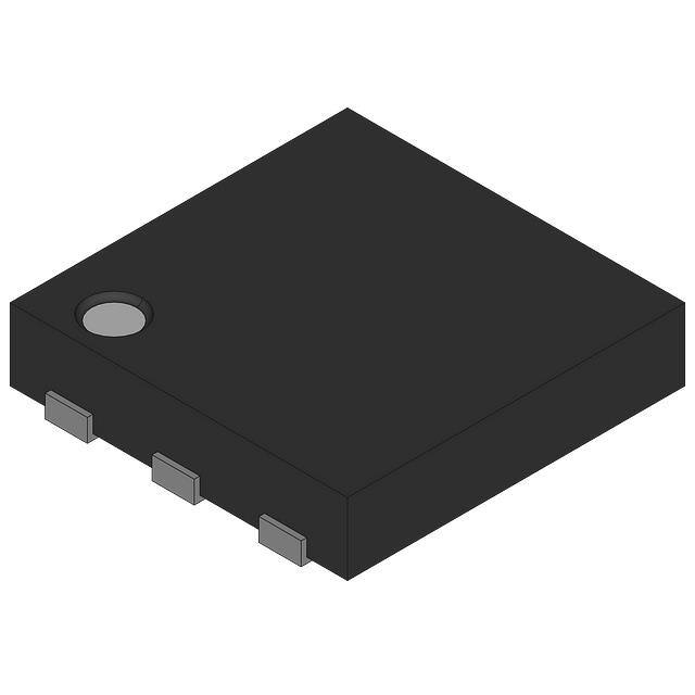
OUTLINE
The RP152x is a 150 mA dual-channel LDO regulator that provides high ripple rejection, low dropout voltage,
high output voltage accuracy, and low supply current. Internally, the RP152x consists of a voltage reference
unit, an error amplifier, resistors for setting output voltage, a short current limit circuit, and a chip enable circuit.
Moreover, the RP152xxxxC consists of a start-up sequence circuit.
The RP152x is available in fixed output voltage options. Besides the low supply current by CMOS, the RP152x
offers a low dropout voltage by built-in low ON resistance Tr. as well as an extended battery life by a chip
enable function. Compared with the existing CMOS-based regulators, the RP152x is further improved in ripple
rejection, line transient response, and load transient response. All these features allow the RP152x to become
ideal power sources for hand-held communication equipment.
The RP152x is offered in a 6-pin SOT-23-6 package and a 6-pin DFN1212-6 package. Both packages are
equipped with two LDOs which can achieve high-density mounting.
FEATURES
•
•
•
•
•
•
•
•
•
•
•
•
Supply Current ························································ Typ. 40 µA x 2
Standby Current ······················································ Typ. 0.1µA x 2
Ripple Rejection ······················································ Typ. 70 dB, f = 1 kHz
Input Voltage Range ················································· 1.4 V to 5.25 V
Output Voltage Range··············································· 0.8 V to 3.6 V, 0.1 V step
Output Voltage Accuracy ··········································· ±1.0%, VSET > 2.0 V, Ta = 25°C
Temperature-Drift Coefficient of Output Voltage ·············· Typ. ±80 ppm/°C
Dropout Voltage······················································· Typ. 0.20 V, IOUT = 150 mA, VSET = 2.8 V
Line Regulation ······················································· Typ. 0.02%/ V
Packages ······························································· DFN1212-6, SOT-23-6
Short-current Limit ··················································· Typ. 40 mA
Ceramic Capacitor Compatible ··································· 0.22 µF or more
APPLICATIONS
•
•
•
Battery-powered Equipment
Portable Communication Equipment, Cameras
Home Electrical Appliances
1
�RP152x
NO.EA-200-160707
SELECTION GUIDE
The set output voltage, the package type, the auto-discharge function 1 and the start-up sequence control are
user-selectable options.
Selection Guide
Product Name
RP152Lxxx∗-TR
RP152Nxxx∗-TR-FE
Package
Quantity per Reel
Pb Free
Halogen Free
DFN1212-6
5,000 pcs
Yes
Yes
SOT-23-6
3,000 pcs
Yes
Yes
xxx: Specify the combination of set output voltage (VSET) within the range of 0.8 V to 3.6 V in 0.1 V step.
∗: Specify the auto-discharge function and the start-up sequence control.
(A) Auto-discharge function not included
(B) Auto-discharge function included
(C) Start-up sequence control and Auto-discharge function included
1 Auto-discharge function quickly lowers the output voltage to 0 V by releasing the electrical charge accumulated in the
external capacitor when the chip enable signal is switched from the active mode to the standby mode.
2
�RP152x
NO.EA-200-160707
BLOCK DIAGRAMS
CE1
VOUT1
CE1
Vref
Vref
R2_1
R2_1
Current Limit
Current Limit
VDD
GND
VDD
GND
R1_2
R1_2
Error Amp.
Error Amp.
Vref
R1_1
Error Amp.
R1_1
Error Amp.
VOUT1
Vref
R2_2
R2_2
Current Limit
Current Limit
CE2
VOUT2
RP152xxxxA Block Diagram
CE1
CE2
VOUT2
RP152xxxxB Block Diagram
VOUT1
Error Amp.
R1_1
Vref
R2_1
Current Limit
VDD
GND
R1_2
100µs
Delay
Error Amp.
Vref
R2_2
Current Limit
CE2
VOUT2
RP152xxxxC Block Diagram
3
�RP152x
NO.EA-200-160707
PIN DESCRIPTIONS
Bottom View
Top View
6
5
4
4
5
6
∗
1
2
3
3
5
4
6
(mark side)
2
1
DFN1212-6 Pin Configuration
DFN1212-6 Pin Description
Pin No.
Symbol
1
2
3
SOT-23-6 Pin Configuration
Description
1
VOUT1
Output Pin 1
2
VOUT2
Output Pin2
3
GND
Ground Pin
4
CE2
Chip Enable Pin 2, Active-high
5
VDD
Input Pin
6
CE1
Chip Enable Pin 1, Active-high
∗ The tab on the bottom of the package enhances thermal performance and is electrically connected to GND (substrate
level). It is recommended that the tab be connected to the ground plane on the board, or otherwise be left floating.
SOT-23-6 Pin Description
Pin No.
Symbol
4
Description
1
CE1
Chip Enable Pin 1, Active-high
2
VDD
Input Pin
3
CE2
Chip Enable Pin 2, Active-high
4
VOUT2
Output Pin2
5
GND
Ground Pin
6
VOUT1
Output Pin 1
�RP152x
NO.EA-200-160707
ABSOLUTE MAXIMUM RATINGS
Absolute Maximum Ratings
Symbol
VIN
VCE
VOUT1
VOUT2
IOUT1
IOUT2
Item
Rating
Unit
Input Voltage
−0.3 to 6.0
V
CE Pin Input Voltage
−0.3 to 6.0
V
Output Voltage
−0.3 to VIN+0.3
V
Output Current
180
mA
DFN1212-6
600
SOT-23-6
420
PD
Power Dissipation (Standard Land Pattern) 1
Tj
Junction Temperature
−40 to 125
°C
Storage Temperature Range
−55 to 125
°C
Tstg
mW
ABSOLUTE MAXIMUM RATINGS
Electronic and mechanical stress momentarily exceeded absolute maximum ratings may cause the permanent
damages and may degrade the life time and safety for both device and system using the device in the field. The
functional operation at or over these absolute maximum ratings is not assured.
RECOMMENDED OPERATING CONDITIONS
Recommended Operating Conditions
Symbol
Item
VIN
Input Voltage
Ta
Operating Temperature Range
2
Rating
Unit
1.40 to 5.25
V
−40 to 85
°C
RECOMMENDED OPERATING CONDITIONS
All of electronic equipment should be designed that the mounted semiconductor devices operate within the
recommended operating conditions. The semiconductor devices cannot operate normally over the recommended
operating conditions, even if when they are used over such conditions by momentary electronic noise or surge. And the
semiconductor devices may receive serious damage when they continue to operate over the recommended operating
conditions.
1
2
Refer to POWER DISSIPATION in SUPPLEMENTARY ITEMS for detailed information.
In case of operating the device beyond 5.25 V, do not exceed 5.5 V with 500 total operating hours.
5
�RP152x
NO.EA-200-160707
ELECTRICAL CHARACTERISTICS
VIN = VSET + 1.0 V (VSET > 1.5 V), VIN = 2.5 V (VSET ≤ 1.5 V), IOUT = 1 mA, CIN = COUT = 0.22 µF, unless otherwise noted.
The specifications surrounded by
are guaranteed by Design Engineering at −40°C ≤ Ta ≤ 85°C.
RP152x Electrical Characteristics
Symbol
(Ta = 25°C)
Item
Conditions
Ta = 25°C
VOUT
Output Voltage
−40°C ≤ Ta ≤ 85°C
IOUT
Min.
Typ.
Max.
Unit
VSET > 2.0 V
×0.99
×1.01
V
VSET ≤ 2.0 V
−20
20
mV
VSET > 2.0 V
×0.97
×1.03
V
VSET ≤ 2.0 V
−60
60
mV
Output Current
mA
150
∆VOUT
/∆IOUT
Load Regulation
1 mA ≤ IOUT ≤ 150 mA
VDIF
Dropout Voltage
IOUT = 150 mA
ISS
Supply Current
IOUT = 0 mA
40
60
µA
Istandby
Standby Current
VCE = 0 V
0.1
1.0
µA
∆VOUT
/∆VIN
Line Regulation
VSET + 0.5 V ≤ VIN ≤ 5.0 V
0.02
0.10
%/V
RR
Ripple Rejection
f = 1 kHz, Ripple 0.2 Vp-p
VIN = VSET + 1.0 V, IOUT = 30 mA
Notes: VIN = 3.0 V when VSET ≤ 2.0 V
70
dB
Output Voltage
Temperature Coefficient
−40°C ≤ Ta ≤ 85°C
±80
ppm
/°C
ISC
Short Current Limit
VSET = 0 V
40
mA
IPD
CE Pull-down Current
0.3
µA
VCEH
CE Input Voltage "H"
VCEL
CE Input Voltage "L"
∆VOUT
/∆Ta
en
RLOW
Refer to Product-specific
Electrical Characteristics
V
1.0
0.4
Output Noise
BW = 10 Hz to 100 kHz
Low Output Nch Tr.
ON Resistance
(RP152xxxxB/C)
VIN = 4.0 V,
VCE = 0 V
60
RP152xxxxC (VR2)
10
Others
50
V
µVrms
Ω
All test items listed under ELECTRICAL CHARACTERISTICS are done under the pulse load condition (Tj ≈Ta = 25°C)
except for Output Noise, Ripple Rejection and Output Voltage Temperature Coefficient.
6
�RP152x
NO.EA-200-160707
Product-specific Electrical Characteristics VOUT1
VOUT1 (Ta = 25°C)
VOUT1 (−40°C ≤ Ta ≤ 85°C)
Product Name
Min.
Typ.
Max.
Min.
Typ.
Max.
RP152x001x
2.772
2.800
2.828
2.716
2.800
2.884
RP152x002x
1.780
1.800
1.820
1.800
1.740
1.860
RP152x003x
1.480
1.500
1.520
1.500
1.440
1.560
RP152x004x
1.180
1.200
1.220
1.140
1.200
1.260
RP152x005x
3.267
3.300
3.333
3.300
3.201
3.399
RP152x006x
3.267
3.300
3.333
3.300
3.201
3.399
RP152x007x
2.822
2.850
2.879
2.850
2.765
2.936
RP152x008x
2.822
2.850
2.879
2.850
2.765
2.936
RP152x009x
2.970
3.000
3.030
2.910
3.000
3.090
RP152x010x
2.970
3.000
3.030
3.000
2.910
3.090
RP152x011x
1.780
1.800
1.820
1.800
1.740
1.860
RP152x012x
2.772
2.800
2.828
2.716
2.800
2.884
RP152x013x
3.267
3.300
3.333
3.300
3.201
3.399
RP152x014x
3.267
3.300
3.333
3.300
3.201
3.399
RP152x015x
1.480
1.500
1.520
1.440
1.500
1.560
RP152x016x
1.480
1.500
1.520
1.500
1.440
1.560
RP152x017x
2.475
2.500
2.525
2.500
2.425
2.575
RP152x018x
1.780
1.800
1.820
1.740
1.800
1.860
RP152x019x
1.480
1.500
1.520
1.500
1.440
1.560
RP152x020x
2.772
2.800
2.828
2.800
2.716
2.884
RP152x021x
1.180
1.200
1.220
1.140
1.200
1.260
RP152x022x
2.772
2.800
2.828
2.800
2.716
2.884
RP152x023x
2.475
2.500
2.525
2.500
2.425
2.575
RP152x024x
3.267
3.300
3.333
3.201
3.300
3.399
RP152x025x
2.970
3.000
3.030
3.000
2.910
3.090
RP152x026x
2.772
2.800
2.828
2.800
2.716
2.884
RP152x027x
2.277
2.300
2.323
2.300
2.231
2.369
RP152x028x
2.772
2.800
2.828
2.800
2.716
2.884
RP152x029x
1.480
1.500
1.520
1.440
1.500
1.560
RP152x030x
1.480
1.500
1.520
1.500
1.440
1.560
RP152x031x
1.780
1.800
1.820
1.800
1.740
1.860
RP152x032x
1.180
1.200
1.220
1.140
1.200
1.260
RP152x033x
3.069
3.100
3.131
3.100
3.007
3.193
RP152x034x
1.780
1.800
1.820
1.800
1.740
1.860
RP152x035x
2.475
2.500
2.525
2.425
2.500
2.575
RP152x036x
1.180
1.200
1.220
1.200
1.140
1.260
RP152x037x
3.267
3.300
3.333
3.300
3.201
3.399
RP152x038x
1.180
1.200
1.220
1.140
1.200
1.260
RP152x039x
2.079
2.100
2.121
2.100
2.037
2.163
RP152x040x
2.772
2.800
2.828
2.800
2.716
2.884
∆VOUT1/ ∆IOUT
Typ. Max.
15
60
15
55
15
50
15
50
15
60
15
60
15
60
15
60
15
60
15
60
15
55
15
60
15
60
15
60
15
50
15
50
15
60
15
55
15
50
15
60
15
50
15
60
15
60
15
60
15
60
15
60
15
60
15
60
15
50
15
50
15
55
15
50
15
60
15
55
15
60
15
50
15
60
15
50
15
60
15
60
VDIF1
Typ.
Max.
0.200 0.350
0.270 0.460
0.310 0.550
0.390 0.620
0.190 0.320
0.190 0.320
0.200 0.350
0.200 0.350
0.190 0.320
0.190 0.320
0.270 0.460
0.200 0.350
0.190 0.320
0.190 0.320
0.310 0.550
0.310 0.550
0.200 0.350
0.270 0.460
0.310 0.550
0.200 0.350
0.390 0.620
0.200 0.350
0.200 0.350
0.190 0.320
0.190 0.320
0.200 0.350
0.230 0.390
0.200 0.350
0.310 0.550
0.310 0.550
0.270 0.460
0.390 0.620
0.190 0.320
0.270 0.460
0.200 0.350
0.390 0.620
0.190 0.320
0.390 0.620
0.230 0.390
0.200 0.350
7
�RP152x
NO.EA-200-160707
Product-specific Electrical Characteristics VOUT1 (continued)
VOUT1 (Ta = 25°C)
VOUT1 (−40°C ≤ Ta ≤ 85°C)
Product Name
Min.
Typ.
Max.
Min.
Typ.
Max.
RP152x041x
1.780
1.800
1.820
1.740
1.800
1.860
RP152x042x
1.180
1.200
1.220
1.200
1.140
1.260
RP152x043x
1.280
1.300
1.320
1.300
1.240
1.360
RP152x044x
1.080
1.100
1.120
1.040
1.100
1.160
RP152x045x
2.772
2.800
2.828
2.800
2.716
2.884
RP152x046x
2.772
2.800
2.828
2.800
2.716
2.884
RP152x047x
2.475
2.500
2.525
2.500
2.425
2.575
RP152x048x
2.475
2.500
2.525
2.500
2.425
2.575
RP152x049x
1.480
1.500
1.520
1.440
1.500
1.560
RP152x050x
2.376
2.400
2.424
2.400
2.328
2.472
RP152x051x
0.980
1.000
1.020
1.000
0.940
1.060
RP152x052x
1.780
1.800
1.820
1.740
1.800
1.860
RP152x053x
2.574
2.600
2.626
2.600
2.522
2.678
RP152x054x
2.475
2.500
2.525
2.500
2.425
2.575
RP152x055x
2.970
3.000
3.030
2.910
3.000
3.090
RP152x056x
2.574
2.600
2.626
2.600
2.522
2.678
RP152x057x
3.069
3.100
3.131
3.100
3.007
3.193
RP152x058x
0.880
0.900
0.920
0.840
0.900
0.960
RP152x059x
2.871
2.900
2.929
2.900
2.813
2.987
RP152x060x
1.180
1.200
1.212
1.200
1.140
1.260
RP152x061x
1.780
1.800
1.820
1.740
1.800
1.860
RP152x062x
2.475
2.500
2.525
2.500
2.425
2.575
8
∆VOUT1/ ∆IOUT
Typ. Max.
15
55
15
50
15
50
15
50
15
60
15
60
15
60
15
60
15
50
15
60
10
40
15
55
15
60
15
60
15
60
15
60
15
60
10
40
15
60
15
50
15
55
15
60
VDIF1
Typ.
Max.
0.270 0.460
0.390 0.620
0.390 0.620
0.440 0.720
0.200 0.350
0.200 0.350
0.200 0.350
0.200 0.350
0.310 0.550
0.230 0.390
0.440 0.720
0.270 0.460
0.200 0.350
0.200 0.350
0.190 0.320
0.200 0.350
0.190 0.320
0.500 0.800
0.200 0.350
0.390 0.620
0.270 0.460
0.200 0.350
�RP152x
NO.EA-200-160707
Product-specific Electrical Characteristics VOUT2
VOUT2 (Ta = 25°C)
VOUT2 (−40°C ≤ Ta ≤ 85°C)
Product Name
Min.
Typ.
Max.
Min.
Typ.
Max.
RP152x001x
2.772
2.800
2.828
2.716
2.800
2.884
RP152x002x
2.772
2.800
2.828
2.800
2.716
2.884
RP152x003x
2.772
2.800
2.828
2.800
2.716
2.884
RP152x004x
1.780
1.800
1.820
1.740
1.800
1.860
RP152x005x
1.180
1.200
1.220
1.200
1.140
1.260
RP152x006x
1.780
1.800
1.820
1.800
1.740
1.860
RP152x007x
2.822
2.850
2.879
2.850
2.765
2.936
RP152x008x
2.574
2.600
2.626
2.600
2.522
2.678
RP152x009x
2.772
2.800
2.828
2.716
2.800
2.884
RP152x010x
1.780
1.800
1.820
1.800
1.740
1.860
RP152x011x
1.480
1.500
1.520
1.500
1.440
1.560
RP152x012x
2.574
2.600
2.626
2.522
2.600
2.678
RP152x013x
2.772
2.800
2.828
2.800
2.716
2.884
RP152x014x
3.267
3.300
3.333
3.300
3.201
3.399
RP152x015x
2.475
2.500
2.525
2.425
2.500
2.575
RP152x016x
2.970
3.000
3.030
3.000
2.910
3.090
RP152x017x
2.970
3.000
3.030
3.000
2.910
3.090
RP152x018x
1.780
1.800
1.820
1.740
1.800
1.860
RP152x019x
2.574
2.600
2.626
2.600
2.522
2.678
RP152x020x
1.780
1.800
1.820
1.800
1.740
1.860
RP152x021x
2.772
2.800
2.828
2.716
2.800
2.884
RP152x022x
1.180
1.200
1.220
1.200
1.140
1.260
RP152x023x
2.475
2.500
2.525
2.500
2.425
2.575
RP152x024x
2.970
3.000
3.030
2.910
3.000
3.090
RP152x025x
2.970
3.000
3.030
3.000
2.910
3.090
RP152x026x
3.069
3.100
3.131
3.100
3.007
3.193
RP152x027x
2.772
2.800
2.828
2.800
2.716
2.884
RP152x028x
0.980
1.000
1.020
1.000
0.940
1.060
RP152x029x
1.480
1.500
1.520
1.440
1.500
1.560
RP152x030x
3.267
3.300
3.333
3.300
3.201
3.399
RP152x031x
2.673
2.700
2.727
2.700
2.619
2.781
RP152x032x
2.970
3.000
3.030
2.910
3.000
3.090
RP152x033x
3.069
3.100
3.131
3.100
3.007
3.193
RP152x034x
2.574
2.600
2.626
2.600
2.522
2.678
RP152x035x
1.180
1.200
1.220
1.140
1.200
1.260
RP152x036x
2.871
2.900
2.929
2.900
2.813
2.987
RP152x037x
1.980
2.000
2.020
2.000
1.940
2.060
RP152x038x
2.822
2.850
2.879
2.765
2.850
2.936
RP152x039x
3.267
3.300
3.333
3.300
3.201
3.399
RP152x040x
2.822
2.850
2.879
2.850
2.765
2.936
∆VOUT2/ ∆IOUT
Typ. Max.
15
60
15
60
15
60
15
55
15
50
15
55
15
60
15
60
15
60
15
55
15
50
15
60
15
60
15
60
15
60
15
60
15
60
15
55
15
60
15
55
15
60
15
50
15
60
15
60
15
60
15
60
15
60
10
40
15
50
15
60
15
60
15
60
15
60
15
60
15
50
15
60
15
60
15
60
15
60
15
60
VDIF2
Typ.
Max.
0.200 0.350
0.200 0.350
0.200 0.350
0.270 0.460
0.390 0.620
0.270 0.460
0.200 0.350
0.200 0.350
0.200 0.350
0.270 0.460
0.310 0.550
0.200 0.350
0.200 0.350
0.190 0.320
0.200 0.350
0.190 0.320
0.190 0.320
0.270 0.460
0.200 0.350
0.270 0.460
0.200 0.350
0.390 0.620
0.200 0.350
0.190 0.320
0.190 0.320
0.190 0.320
0.200 0.350
0.440 0.720
0.310 0.550
0.190 0.320
0.200 0.350
0.190 0.320
0.190 0.320
0.200 0.350
0.390 0.620
0.200 0.350
0.270 0.460
0.200 0.350
0.190 0.320
0.200 0.350
9
�RP152x
NO.EA-200-160707
Product-specific Electrical Characteristics VOUT2 (continued)
VOUT2 (Ta = 25°C)
VOUT2 (−40°C ≤ Ta ≤ 85°C)
Product Name
Min.
Typ.
Max.
Min.
Typ.
Max.
RP152x041x
2.970
3.000
3.030
2.910
3.000
3.090
RP152x042x
2.574
2.600
2.626
2.600
2.522
2.678
RP152x043x
2.772
2.800
2.828
2.800
2.716
2.884
RP152x044x
1.480
1.500
1.520
1.440
1.500
1.560
RP152x045x
3.267
3.300
3.333
3.300
3.201
3.399
RP152x046x
2.970
3.000
3.030
3.000
2.910
3.090
RP152x047x
2.772
2.800
2.828
2.800
2.716
2.884
RP152x048x
3.168
3.200
3.232
3.200
3.104
3.296
RP152x049x
2.822
2.850
2.879
2.765
2.850
2.936
RP152x050x
2.871
2.900
2.929
2.900
2.813
2.987
RP152x051x
1.780
1.800
1.820
1.800
1.740
1.860
RP152x052x
2.822
2.850
2.879
2.765
2.850
2.936
RP152x053x
2.673
2.700
2.727
2.700
2.619
2.781
RP152x054x
1.780
1.800
1.820
1.800
1.740
1.860
RP152x055x
2.822
2.850
2.879
2.765
2.850
2.936
RP152x056x
2.970
3.000
3.030
3.000
2.910
3.090
RP152x057x
1.780
1.800
1.820
1.800
1.740
1.860
RP152x058x
0.880
0.900
0.920
0.840
0.900
0.960
RP152x059x
2.871
2.900
2.929
2.900
2.813
2.987
RP152x060x
1.180
1.200
1.212
1.200
1.140
1.260
RP152x061x
2.871
2.900
2.929
2.813
2.900
2.987
RP152x062x
3.069
3.100
3.131
3.100
3.007
3.193
10
∆VOUT2/ ∆IOUT
Typ. Max.
15
60
15
60
15
60
15
50
15
60
15
60
15
60
15
60
15
60
15
60
15
55
15
60
15
60
15
55
15
60
15
60
15
55
10
40
15
60
15
50
15
60
15
60
VDIF2
Typ.
Max.
0.190 0.320
0.200 0.350
0.200 0.350
0.310 0.550
0.190 0.320
0.190 0.320
0.200 0.350
0.190 0.320
0.200 0.350
0.200 0.350
0.270 0.460
0.200 0.350
0.200 0.350
0.270 0.460
0.200 0.350
0.190 0.320
0.270 0.460
0.500 0.800
0.200 0.350
0.390 0.620
0.200 0.350
0.190 0.320
�RP152x
NO.EA-200-160707
THEORY OF OPERATION
Start-up Sequence Circuit
The RP152xxxxC is equipped with a start-up sequence circuit. VR2 stands-up in 100 µs delay after VR1 stands
up simultaneously with CE. Moreover, to disabling is depending upon the setting output voltage and the
external capacitors. VR1 reduces the output voltage by the Nch driver of about 50 Ω, and VR2 reduces the
output voltage by the Nch driver of about 10 Ω.
CE1&CE2
VOUT1
100 µs delay
50 Ω Discharge
10 Ω Discharge
VOUT2
RP152xxxxC Start-up Sequence Circuit
11
�RP152x
NO.EA-200-160707
APPLICATION INFORMATION
CE2
VOUT2
VOUT2
RP152x
VIN
CIN
VDD
GND
CE1
VOUT1
COUT2
VOUT1
COUT1
RP152x Typical Application Circuit
External Components
Symbol
Description
CIN
COUT1
Ceramic, 0.22 µF, Murata: GRM155B31A224KE18B
COUT2
Technical Notes on the Components Selection
•
In this device, phase compensation is provided to secure stable operation even when the load current
varied. For this purpose, connect 0.22 μF or more output capacitors (COUT1, COUT2) between the VOUT
and GND pin with shortest-distance wiring. In case of using a tantalum type capacitor and the ESR
(Equivalent Series Resistance) value of the capacitor is large, the output might be unstable. Evaluate the
circuit including consideration of frequency characteristics.
•
Ensure the VDD and GND lines are sufficiently robust. If their impedance is too high, noise pickup or
unstable operation may result. Connect a 0.22 μF input capacitor (CIN) between the VDD and GND pins
with shortest-distance wiring. Refer to Typical Application Circuit.
12
�RP152x
NO.EA-200-160707
TYPICAL CHARACTERISTICS
Notes: Typical Characteristics are intended to be used as reference data; they are not guaranteed.
1) Output Voltage vs. Output Current (Ta = 25°C)
0.8 V (VR1/ VR2)
2.5 V (VR1/ VR2)
3.6 V (VR1/ VR2)
2) Output Voltage vs. Input Voltage (Ta = 25°C)
0.8 V (VR1/ VR2)
2.5 V (VR1/ VR2)
13
�RP152x
NO.EA-200-160707
3.6 V (VR1/ VR2)
3) Supply Current vs. Input Voltage
0.8 V (VR1/ VR2)
3.6 V (VR1/ VR2)
14
2.5 V (VR1/ VR2)
�RP152x
NO.EA-200-160707
4) Output Voltage vs. Temperature
0.8 V (VR1/ VR2)
VIN = 1.8 V
2.5 V (VR1/ VR2)
VIN = 3.5 V
3.6 V (VR1/ VR2)
VIN = 4.6 V
5) Supply Current vs. Temperature
0.8 V (VR1/ VR2)
VIN = 1.8 V
2.5 V (VR1/ VR2)
VIN = 3.5 V
15
�RP152x
NO.EA-200-160707
3.6V(VR1/VR2)
VIN = 4.6 V
6) Dropout Voltage vs. Output Current
0.8 V (VR1/ VR2)
3.6 V (VR1/ VR2)
16
2.5 V (VR1/ VR2)
�RP152x
NO.EA-200-160707
7) Dropout Voltage vs. Set Output Voltage
8) Minimum Operating Voltage
0.8 V (VR1/ VR2)
The hatched area is available
for a 0.8-V output device.
9) Ripple Rejection vs. Input Voltage
(CIN = none, COUT1 = COUT2 = Ceramic 0.22 µF, Ripple = 0.2 Vp-p, Ta = 25°C)
2.5 V (VR1/ VR2)
2.5 V (VR1/ VR2)
17
�RP152x
NO.EA-200-160707
10) Ripple Rejection vs. Frequency
(CIN = none, COUT1 = COUT2 = Ceramic 0.22 µF, Ripple = 0.2 Vp-p, Ta = 25°C)
0.8 V (VR1/ VR2)
2.5 V (VR1/ VR2)
3.6 V (VR1/ VR2)
11) Input Transient Response
(IOUT = 30 mA, tr = tf = 5 µs, CIN = none, COUT1 = COUT2 = 0.22 µF, Ta = 25°C)
0.8 V (VR1/ VR2)
2.5 V (VR1/ VR2)
18
�RP152x
NO.EA-200-160707
3.6 V (VR1/ VR2)
12) Load Transient Response (tr = tf = 0.5 µs, CIN = COUT1 = COUT2 = 0.22 µF, Ta = 25°C)
0.8 V (VR1/ VR2)
0.8 V (VR1/ VR2)
0.8 V (VR1/ VR2)
0.8 V (VR1/ VR2)
19
�RP152x
NO.EA-200-160707
2.5 V (VR1/ VR2)
20
2.5 V (VR1/ VR2)
2.5 V (VR1/ VR2)
2.5 V (VR1/ VR2)
3.6 V (VR1/ VR2)
3.6 V (VR1/ VR2)
�RP152x
NO.EA-200-160707
3.6 V (VR1/ VR2)
3.6 V (VR1/ VR2)
13) Turn On Speed with CE Pin (CIN = COUT1 = COUT2 = 0.22 µF, Ta = 25°C)
0.8 V A/B Version (VR1/ VR2), C Version (VR1)
0.8 V C Version (VR2)
2.5 V A/B Version (VR1/ VR2), C Version (VR1)
2.5 V C Version (VR2)
21
�RP152x
NO.EA-200-160707
3.6 V A/B Version (VR1/ VR2), C Version (VR1)
3.6 V C Version (VR2)
14) Tum Off Speed with CE Pin (CIN = COUT1 = COUT2 = 0.22 µF, Ta = 25°C)
0.8 V B Version (VR1/ VR2), C Version (VR1)
0.8 V C Version (VR2)
2.5 V B Version (VR1/ VR2), C Version (VR1)
22
2.5 V C Version (VR2)
�RP152x
NO.EA-200-160707
3.6 V B Version (VR1/ VR2), C Version (VR1)
3.6 V C Version (VR2)
23
�RP152x
NO.EA-200-160707
Equivalent Series Resistance (ESR) vs. Output Current
It is recommended that a ceramic type capacitor be used for the RP152x. However, other types of capacitors
having lower ESR can also be used. The relation between the output current (IOUT) and the ESR of output
capacitor is shown below.
Measurement Conditions:
•
•
•
•
Noise Frequency Band: 10 Hz to 2 MHz
Measurement Temperature: −40°C to +85°C
Hatched Area: Noise level is 40 µV (avg.) or below.
CIN, COUT1, COUT2: 0.22 µF (Murata: GRM155B10J224KE01)
0.8 V (VR1/ VR2)
VIN = 1.4 V to 5.0 V
Ta = 85°C
2.5 V (VR1/ VR2)
VIN = 2.6 V to 5.0 V
Ta = 85°C
Ta = −40°C
Ta = −40°C
3.6 V (VR1/ VR2)
VIN = 3.7 V to 5.0 V
Ta = 85°C
Ta = −40°C
24
�POWER DISSIPATION
DFN1212-6
Ver. A
Power Dissipation (PD) of the package is dependent on PCB material, layout, and environmental conditions.
The following conditions are used in this measurement.
Measurement Conditions
Standard Land Pattern
Environment
Mounting on Board (Wind Velocity = 0 m/s)
Board Material
Glass Cloth Epoxy Plastic (Double-sided)
Board Dimensions
40 mm x 40 mm x 1.6 mm
Copper Ratio
Top-side: Approx. 50%, Back-side: Approx. 50%
Through-holes
: 0.5 mm x 28 pcs
Measurement Result
(Ta = 25C, Tjmax = 125C)
Standard Land Pattern
Power Dissipation
600 mW
ja = (125 − 25°C) / 0.6 W = 167°C/W
Thermal Resistance
jc = 30°C/W
40
600
On Board
500
400
300
40
Power Dissipation PD (mW)
700
200
100
0
0
25
50
75 85 100
125
Ambient Temperature (°C)
Power Dissipation vs. Ambient Temperature
150
IC Mount Area (Unit: mm)
Measurement Board Pattern
i
�PACKAGE DIMENSIONS
DFN1212-6
0.940.05
4
6
※
1.20
0.05
C0.15
0.300.05
INDEX
3
0.40
1
0.180.05
Bottom View
S
0.200.05
B
0.4max
X4
1.20
0.05 S
0.05
A
0.200.05
Ver. A
0.05
M
AB
(Unit: mm)
※ The tab on the bottom of the package enhances thermal
performance and is electrically connected to GND (substrate
level). It is recommended that the tab be connected to the
ground plane on the board, or otherwise be left floating.
DFN1212-6 Package Dimensions
i
�POWER DISSIPATION
SOT-23-6
Ver. A
Power Dissipation (PD) of the package is dependent on PCB material, layout, and environmental conditions.
The following conditions are used in this measurement.
Measurement Conditions
Standard Land Pattern
Environment
Mounting on Board (Wind Velocity = 0 m/s)
Board Material
Glass Cloth Epoxy Plastic (Double-sided)
Board Dimensions
40 mm x 40 mm x 1.6 mm
Copper Ratio
Top-side: Approx. 50%, Back-side: Approx. 50%
Through-holes
0.5 mm x 44 pcs
Measurement Result
(Ta = 25C, Tjmax = 125C)
Standard Land Pattern
Free Air
Power Dissipation
420 mW
250 mW
Thermal Resistance
ja = (125 - 25C) / 0.42 W = 238C/W
400C/W
40
500
420
On Board
400
300
Free Air
250
40
Power Dissipation PD (mW)
600
200
100
0
0
25
50
75 85 100
125
150
Ambient Temperature (C)
Power Dissipation (mW) vs. Temperature (°C)
IC Mount Area (Unit: mm)
Measurement Board Pattern
i
�PACKAGE DIMENSIONS
SOT-23-6
Ver. A
2.9±0.2
+0.2
1.1-0.1
1.9±0.2
4
1
2
0 to 0.1
0.2MIN.
5
+0.2
1.6-0.1
6
0.8±0.1
(0.95)
2.8±0.3
(0.95)
3
+0.1
0.4-0.2
+0.1
0.15-0.05
Unit : mm
SOT-23-6 Package Dimensions
i
�1. The products and the product specifications described in this document are subject to change or discontinuation of
production without notice for reasons such as improvement. Therefore, before deciding to use the products, please
refer to Ricoh sales representatives for the latest information thereon.
2. The materials in this document may not be copied or otherwise reproduced in whole or in part without prior written
consent of Ricoh.
3. Please be sure to take any necessary formalities under relevant laws or regulations before exporting or otherwise
taking out of your country the products or the technical information described herein.
4. The technical information described in this document shows typical characteristics of and example application circuits
for the products. The release of such information is not to be construed as a warranty of or a grant of license under
Ricoh's or any third party's intellectual property rights or any other rights.
5. The products listed in this document are intended and designed for use as general electronic components in standard
applications (office equipment, telecommunication equipment, measuring instruments, consumer electronic products,
amusement equipment etc.). Those customers intending to use a product in an application requiring extreme quality
and reliability, for example, in a highly specific application where the failure or misoperation of the product could result
in human injury or death (aircraft, spacevehicle, nuclear reactor control system, traffic control system, automotive and
transportation equipment, combustion equipment, safety devices, life support system etc.) should first contact us.
6. We are making our continuous effort to improve the quality and reliability of our products, but semiconductor products
are likely to fail with certain probability. In order to prevent any injury to persons or damages to property resulting from
such failure, customers should be careful enough to incorporate safety measures in their design, such as redundancy
feature, fire containment feature and fail-safe feature. We do not assume any liability or responsibility for any loss or
damage arising from misuse or inappropriate use of the products.
7. Anti-radiation design is not implemented in the products described in this document.
8. The X-ray exposure can influence functions and characteristics of the products. Confirm the product functions and
characteristics in the evaluation stage.
9. WLCSP products should be used in light shielded environments. The light exposure can influence functions and
characteristics of the products under operation or storage.
10. There can be variation in the marking when different AOI (Automated Optical Inspection) equipment is used. In the
case of recognizing the marking characteristic with AOI, please contact Ricoh sales or our distributor before attempting
to use AOI.
11. Please contact Ricoh sales representatives should you have any questions or comments concerning the products or
the technical information.
Halogen Free
Ricoh is committed to reducing the environmental loading materials in electrical devices
with a view to contributing to the protection of human health and the environment.
Ricoh has been providing RoHS compliant products since April 1, 2006 and Halogen-free products since
April 1, 2012.
https://www.e-devices.ricoh.co.jp/en/
Sales & Support Offices
Ricoh Electronic Devices Co., Ltd.
Shin-Yokohama Office (International Sales)
2-3, Shin-Yokohama 3-chome, Kohoku-ku, Yokohama-shi, Kanagawa, 222-8530, Japan
Phone: +81-50-3814-7687 Fax: +81-45-474-0074
Ricoh Americas Holdings, Inc.
675 Campbell Technology Parkway, Suite 200 Campbell, CA 95008, U.S.A.
Phone: +1-408-610-3105
Ricoh Europe (Netherlands) B.V.
Semiconductor Support Centre
Prof. W.H. Keesomlaan 1, 1183 DJ Amstelveen, The Netherlands
Phone: +31-20-5474-309
Ricoh International B.V. - German Branch
Semiconductor Sales and Support Centre
Oberrather Strasse 6, 40472 Düsseldorf, Germany
Phone: +49-211-6546-0
Ricoh Electronic Devices Korea Co., Ltd.
3F, Haesung Bldg, 504, Teheran-ro, Gangnam-gu, Seoul, 135-725, Korea
Phone: +82-2-2135-5700 Fax: +82-2-2051-5713
Ricoh Electronic Devices Shanghai Co., Ltd.
Room 403, No.2 Building, No.690 Bibo Road, Pu Dong New District, Shanghai 201203,
People's Republic of China
Phone: +86-21-5027-3200 Fax: +86-21-5027-3299
Ricoh Electronic Devices Shanghai Co., Ltd.
Shenzhen Branch
1205, Block D(Jinlong Building), Kingkey 100, Hongbao Road, Luohu District,
Shenzhen, China
Phone: +86-755-8348-7600 Ext 225
Ricoh Electronic Devices Co., Ltd.
Taipei office
Room 109, 10F-1, No.51, Hengyang Rd., Taipei City, Taiwan (R.O.C.)
Phone: +886-2-2313-1621/1622 Fax: +886-2-2313-1623
�


 工商网监
湘ICP备2023018690号
工商网监
湘ICP备2023018690号
