LED Drivers for LED Decoration
LED Driver for Indicators and Signage
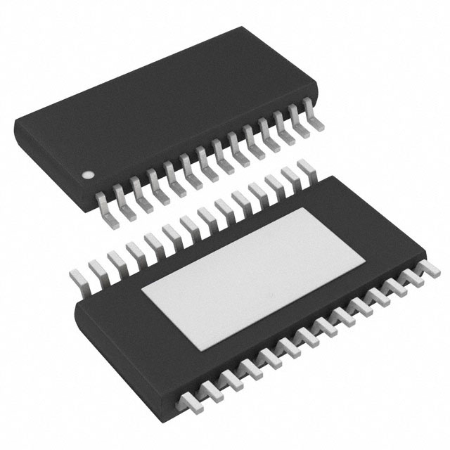
BD7844AEFV
No.11107EAT01
●Description BD7844AEFV is LED Display Driver. It can control 16ch Nch Open Drain output for LED drive. It can control the luminance of 2 the LEDs by the setting of the internal register, with 256 steps PWM control. It supports I C interface. HTSSOP-B28 (with Back-side metal for heat radiation) package. ●Features 1) 16ch × 80mA (Absolute Maximum Rating) 2 2) Conforming to I C -bus I/F (1MHz Fast mode Plus) 3) Either of interactive or single direction can be selected with the I2CSEL pin. (2MHz clock frequency on single direction) 4) Independent setting of output brightness is possible by register setting for each channel. (PWM 256 steps) 5) Power supply voltage : 4.5 ~ 5.5V 6) Max voltage of Open-drain output terminals: 20.0V (Absolute Maximum Rating) 7) Built-in thermal shutdown (TSD)circuit 8) Built-in power-on reset circuit 9) Small package with back-side metal for heat radiation: HTSSOP-B28 ●Absolute Maximum Ratings (Ta=25℃) Parameter Power supply voltage Operating voltage range Output terminal voltage Output terminal current Logic input terminal voltage Permissible dissipation Operating temperature range Storage temperature range Junction temperature Symbol VDDMAX1 VDDMAX2 VOUTMAX IOUTMAX VINMAX Pd Topr Tstr Tjmax Ratings Unit V V V mA/ch V W ℃ ℃ ℃
-0.3 -0.3 -0.3
~ 7.0
4.5 ~ 5.5 ~ 20.0 80
*1
~ VDD+0.3 ≦ 7.0 1.45
*2
-40 ~ 85 -55 ~ 150
150
Please be careful that the anti-radiation design is not applied to this IC. *1) Please take the IC’s power consumption & permissible dissipation into consideration before using it. *2) Mounted on ROHM standard board (70mm×70mm×1.6mm (thickness), glass-epoxy board). Ta=25℃ or more, it is reduced with 11.6mW/℃.
●Operating conditions (Ta=-40~85℃) Parameter Power supply voltage High level input voltage Low level input voltage Low level output current Symbol VDD VIH VIL IOL Ratings 4.5 ~ 5.5 VDDx0.7 ~ VDD 0 ~ VDDx0.3 ~ 30 Unit V V V mA SDA,SCL,RESETB, I2CSEL,A0,A1,A2,A3 SDA Conditions
www.rohm.com © 2011 ROHM Co., Ltd. All rights reserved.
1/13
2011.07 - Rev.A
�BD7844AEFV
●Electrical Characteristics (Unless otherwise specified, Ta=25℃, VDD=5.0V, GND=0V) Limits Parameter Symbol Min. Typ. Max. VDD Circuit current1(All ch OFF) VDD Circuit current2(All ch full ON) Input/Output leak current Pull Up Resistor Output pin leak current Power On Reset voltage Low level output current Low level output voltage Resistor at ON Input capacitance I/O capacitance IDD1 IDD2 ILEAK1 RRSTB RI2C ILEAK2 VPOR IOL VOL RON Ci Cio - - - 30 55 - - 30 - - - - 8.7 9.5 - 60 110 - 2.4 - 200 2.5 6 12 11.9 13.0 1.0 90 165 1.0 - - 550 6.875 - -
Technical Note
Unit mA mA µA kΩ kΩ µA V mA mV Ω pF pF
Conditions Input pin fixed Input pin fixed SDA,SCL,A0,A1,A2,A3 VIN = VDD or GND RESETB I2CSEL OUT0 ~ OUT15 VOUT = 20V SDA VOL = 0.4V OUT0 ~ OUT15 IOUT = 80mA OUT0 ~ OUT15 IOUT = 80mA SCL,RESETB,I2CSEL, A0,A1,A2,A3 SDA
●Logic signal timing specification (Unless otherwise specified, Ta=25℃, VDD=5.0V, GND=0V) Limits Parameter Symbol Unit Min. Typ. Max. SCL Clock frequency 1 SCL Clock frequency 2 Bus free time between a STOP and START condition *1 Hold time (repeated) START condition. After this period, the first clock is generated Set-up time for a repeated START condition Set-up time for STOP condition SDA Data hold time SDA data valid acknowledge time SDA data valid time *3 SDA Data set-up time SCL clock low period1 SCL clock high period1 SCL, SDA fall time1 SCL, SDA rise time1 SCL clock low period2 SCL clock high period2 SCL, SDA fall time2 SCL, SDA rise time2 Pulse width of spikes which must be suppressed by SCL, SDA filter Reset pulse width *4
*1) *2) *3) *4)
*2
Conditions I2CSEL=H : SDA=I/O I2CSEL =L : SDA=input
fSCL1 fSCL2 tBUF tHD;STA tSU;STA tSU;STO tHD;DAT tVD;ACK tVD;DAT tSU;DAT tLOW1 tHIGH1 tf1 tr1 tLOW2 tHIGH2 tf2 tr2 tSP tW
500 260 260 260 0 50 500 260 230 250 -
50 10
1.0 2.0 450 450 120 120 50 50 -
MHz MHz ns ns ns ns ns ns ns ns ns ns ns ns ns ns ns ns ns ns
I2CSEL =H : SDA=I/O I2CSEL =H : SDA=I/O
I2CSEL =H : SDA=I/O I2CSEL =H : SDA=I/O I2CSEL =H : SDA=I/O I2CSEL =H : SDA=I/O I2CSEL =L : SDA=input I2CSEL =L : SDA=input I2CSEL =L : SDA=input I2CSEL =L : SDA=input
Keep more than 100us Bus free time after power on. tVD;ACK :Time for acknowledge signal from SCL=’L’ to SDA(output)=’L’ tVD;DAT :Time for from SCL=’L’ to SDA valid data output Miss-operation is likely to happen with reset in accessing I2C bus.
www.rohm.com © 2011 ROHM Co., Ltd. All rights reserved.
2/13
2011.07 - Rev.A
�BD7844AEFV
●Block Diagram / Application Circuit example
Technical Note
4.5V – 5.5V VLED Max 20V VDD
I2CSEL A0 A1 A2 A3
NDMOS Output (Sink Type) Logic Enable PWM1 OUT0 PWM0
OUT1
SDA SCL
I2C Filter 16MHz VCO RESETB
PWM14 OUT14 PWM15 OUT15
RESETB POR TSD
GND
GND
GND
Fig.1
Block Diagram / Application Circuit example
www.rohm.com © 2011 ROHM Co., Ltd. All rights reserved.
3/13
2011.07 - Rev.A
�BD7844AEFV
●Pin Arrangement [Top View]
Technical Note
Fig.2 Pin arrangement ●Pin Functions Pin No 1 2 3 4 5 6 7 8 9 10 11 12 13 14 15 16 17 18 19 20 21 22 23 24 25 26 27 28 Pin Name I2CSEL A0 A1 A2 A3 OUT0 OUT1 OUT2 OUT3 GND OUT4 OUT5 OUT6 OUT7 OUT8 OUT9 OUT10 OUT11 GND OUT12 OUT13 OUT14 OUT15 GND RESETB SCL SDA VDD I/O I I I I I O O O O O O O O O O O O O O O O I I I/O Pull up Register 110kΩ 60kΩ Unused Terminal setting GND GND GND GND GND GND GND GND GND GND GND GND GND GND GND GND GND GND GND GND GND GND GND GND GND GND GND GND ESD Diode For Power VDD VDD VDD VDD VDD VDD VDD VDD VDD For Ground GND GND GND GND GND GND GND GND GND GND GND GND GND GND GND GND GND GND GND GND GND GND GND GND GND Functions I2C access mode select for SDA (H: I/O, L: Input only) Slave address setting Slave address setting Slave address setting Slave address setting Open Drain output Open Drain output Open Drain output Open Drain output Ground Open Drain output Open Drain output Open Drain output Open Drain output Open Drain output Open Drain output Open Drain output Open Drain output Ground Open Drain output Open Drain output Open Drain output Open Drain output Ground Reset input pin (L: reset, H: reset cancel) Serial clock input pin Serial data I/O pin Power supply
* Please connect the unused LED pins to the ground. * It is prohibition to set the registers for unused LED.
www.rohm.com © 2011 ROHM Co., Ltd. All rights reserved.
4/13
2011.07 - Rev.A
�BD7844AEFV
●Definition of logic signal timing
START SCL ACK OR READ CYCLE
Technical Note
SDA
30% tRESET
30%
RESET* tREC
50% tW
50%
tRESET OUTx 50%
LED OFF
SDA
tBUF tLOW
tr tf
tHD:STA
tSP
SCL
tHD:STA P S tHD:DAT tHIGH tSU:DAT Sr
tSU:STA
tSU:STO P
protocol
START Condition (S)
bit 7 MSB (A7)
bit 6 (A7)
bit 7 (D1)
bit 8 (D0)
acknowledge (A)
STOP condition (P)
tSU:STA
tLOW
tHIGH 1/fSCL
SCL
tr
tf
tBUF
SDA
tHD:STA
tSU:DAT
tHD:DAT
tVD:DAT
tVD:ACK
tSU:STO
Fig.3 Definition of logic signal timing
www.rohm.com © 2011 ROHM Co., Ltd. All rights reserved.
5/13
2011.07 - Rev.A
�BD7844AEFV
Technical Note
●Logic Function explaining 1. Slave address LED driver BD7844AEFV is a slave device. The master device outputs the transmission clock and the transmission data, and BD7844AEFV who is the slave returns the acknowledgement. The master device transmits the slave address of BD7844AEFV following the START condition. Afterwards, BD7844AEFV can be controlled in the command by transmitting the register address and the register data continuously, and doing the transmission completion under the 2 STOP condition. Fig. 4 shows basic format (I C) of the control command of BD7844AEFV. Master transmits data Master receives data “0” = Write S Slave address Slave address R/W A Register address Register address A Register data Slave address Register data A
P
“0” = Write S R/W A A S
S=START, P=STOP
From master to slave From slave to master
“1” = Read R/W A A P
2 Fig. 4 Basic format of control command(I C)
BD7844AEFV has three kinds of slave addresses (for usually, for all calls, and for software reset). 1-1. Usual slave address Fig. 5 shows the slave address of BD7844AEFV. Because an internal pull-up resistor has not placed to the address terminal (A[3:0]) that can be selected with hardware to save power consumption, it is necessary to connect them with high ( =VDD ) or low ( =GND ). Slave address
1
0
1
A3
A2
A1
A0
R/W
Fixed
It is optional with the address terminal Fig. 5 Usual slave address
The last RW bit of the slave address byte defines the executed operation. Reading is selected when setting it to logic 1, and writing is selected when setting it to logic 0. Fixed 101 101 101 101 101 101 101 101 101 101 101 101 101 101 101 101 A3 0 0 0 0 0 0 0 0 1 1 1 1 1 1 1 1 A2 0 0 0 0 1 1 1 1 0 0 0 0 1 1 1 1 A1 0 0 1 1 0 0 1 1 0 0 1 1 0 0 1 A0 0 1 0 1 0 1 0 1 0 1 0 1 0 1 0 R/W R/W R/W R/W R/W R/W R/W R/W R/W R/W R/W R/W 0 R/W R/W R/W R/W Function Usual 1 Usual 2 Usual 3 Usual 4 Usual 5 Usual 6 Usual 7 Usual 8 All call Usual 9 Usual 10 Software reset Usual 11 Usual 12 Usual 13 Usual 14
1 1 Table 1. Slave address
www.rohm.com © 2011 ROHM Co., Ltd. All rights reserved.
6/13
2011.07 - Rev.A
�BD7844AEFV
1-2. Slave address for all call [1011000] is used as a slave address for all call. (Fig. 6) Slave address for all call
Technical Note
1
0
1
1
0
0
0
R/W
Unavailable in address terminal Fig. 6 Slave address for all call All BD7844AEFV on the bus can control in the command at the same time by the slave address for all call. It enters the state that can respond to all call when power supply (VDD) is turned on. It can be selected not to respond when the ALL CALL bit of mode1 register is set to logic “0”. Because the register data is returned from all BD7844AEFV on the bus when the last R/W bit of the slave address byte is set to logic "1" (read) when the slave address for all calls is used, the master cannot read the register data of specific BD7844AEFV. Please use a usual slave address to read the register data of specific BD7844AEFV. Take care: Slave address [1011000] for all calls must not use as a usual slave address because it becomes enable when power supply (VDD) is turned on.
1-3. Slave address for software reset [1011011] is used as a slave address for software reset. (Fig. 7) Slave address for software reset R/W
1
0
1
1
0
1
1
0
Unavailable in address terminal Fig. 7 Slave address for software reset All BD7844AEFV on the bus can be reset at the same time by the slave address for software reset. It is necessary to use the slave address for software reset with R/W=0. BD7844AEFV doesn't recognize software reset for R/W=1. Please refer to "3-2. Software reset" for details. Take care: Because slave address [1011011] for software reset is a reserved address, It is not possible to use it as a usual slave address.
www.rohm.com © 2011 ROHM Co., Ltd. All rights reserved.
7/13
2011.07 - Rev.A
�BD7844AEFV
Technical Note
2. Register address After completing the acknowledgement of the slave address, the master device transmits the register address to BD7844AEFV. Fig. 8 shows the register address. Auto increment option
AI 2
AI 1
AI 0
RA 4
RA 3
RA 2
RA 1
RA 0
Register address Fig. 8 Register address The auto increment option is specified for MSB 3bit.The address of the register that wants to be controlled is specified for LSB 5bit. Sending register data continuously with the auto increment option in the three high rank bits can continuously set each brightness control register. (Mode1 register cannot be set by the auto increment option.) The register of BD7844AEFV is shown in Table 2 and the auto increment option is shown in Table 3 Register address(Hex) 00 01 02 03 04 05 06 07 08 09 0A 0B 0C 0D 0E 0F 1A* Register name PWM0 [7:0] PWM1 [7:0] PWM2 [7:0] PWM3 [7:0] PWM4 [7:0] PWM5 [7:0] PWM6 [7:0] PWM7 [7:0] PWM8 [7:0] PWM9 [7:0] PWM10 [7:0] PWM11 [7:0] PWM12 [7:0] PWM13 [7:0] PWM14 [7:0] PWM15 [7:0] MODE1 [7:0] Initial Value after reset 00h 00h 00h 00h 00h 00h 00h 00h 00h 00h 00h 00h 00h 00h 00h 00h 03h Access R/W R/W R/W R/W R/W R/W R/W R/W R/W R/W R/W R/W R/W R/W R/W R/W R/W Table 2. Register AI2 0 0 0 0 1 1 1 1 AI1 0 0 1 1 0 0 1 1 AI0 0 1 0 1 0 1 0 1 Table 3. Auto increment option Prohibited Auto increment none Address auto increment (+1) for brightness control register PWM0~15only. Function Function Brightness control (256steps) OUT0 Brightness control (256steps) OUT1 Brightness control (256steps) OUT2 Brightness control (256steps) OUT3 Brightness control (256steps) OUT4 Brightness control (256steps) OUT5 Brightness control (256steps) OUT6 Brightness control (256steps) OUT7 Brightness control (256steps) OUT8 Brightness control (256steps) OUT9 Brightness control (256steps) OUT10 Brightness control (256steps) OUT11 Brightness control (256steps) OUT12 Brightness control (256steps) OUT13 Brightness control (256steps) OUT14 Brightness control (256steps) OUT15 Mode 1 setting
*MODE1 register cannot be set by the auto increment option.
www.rohm.com © 2011 ROHM Co., Ltd. All rights reserved.
8/13
2011.07 - Rev.A
�BD7844AEFV
Technical Note
2-1. PWM0 ~ PWM15 register data The brightness of output terminal OUT0 ~ OUT15 is set by the register data of PWM0(address:00h) ~ PWM15(address:0Fh). The PWM brightness control in 256 steps is possible from 00h (complete off) to FFh (complete on). 2-2. Mode1 registers data The operation mode of BD7844AEFV is set according to mode1 register (address: 1Ah) data. Table 4 shows the allocation of the bit of mode1 register data. Bit 7 6 5 4 3 2 1 0 Bit name LIMITRESET PROTECT0 Reservation PWMSLOW Reservation Reservation PROTECT1 ALLCALL Access R/W R/W R/W R/W R/W R/W R/W R/W Value 0* 1 0 0 0
*
Function Device limitation software reset : off Device limitation software reset : on Please write “0”. It is not recognized as Mode1 register data at “1”. Please write “0” Prohibited PWM period is 60kHz PWM period is 2kHz Please write “0”. Prohibited Please write “0”. Prohibited Please write “1”. It is not recognized as Mode1 register data at “0”. It doesn't respond to the slave address for all call. It responds to the slave address for all call.
1
*
1 0* 1 0* 1 1 0 1*
*Default value after reset
Table 4. Mode1 register (Address: 1Ah) data Mode1 register data cannot be set by the auto increment option. Please set it alone by the following format. In the correct execution, there should not be device that monopolizes the bus. 2-3. Mode1 register data setting procedure 2 1. The START condition is sent by the I C bus master. 2. The slave address of BD7844AEFV that wants to be set by mode1 register is sent by the master. 3. When the slave address is sent and recognized, the master sends mode1 register address [00011010] (1Ah). It is recognized only when LSB 5bit are [11010] and the auto increment option in MSB 3bit are [000]. 4. When mode1 register address is sent and recognized, the master sends mode1 register data. It recognizes it as data only when the data confirmation bit (bit 6=0 and bit1=1) is all correct. 5. When correct mode1 register data is sent and recognized, the master sends the STOP condition to end mode1 setting command. Afterwards, LIMITRESET, PWMSLOW, and ALLCALL become effective.
www.rohm.com © 2011 ROHM Co., Ltd. All rights reserved.
9/13
2011.07 - Rev.A
�BD7844AEFV
3. Reset BD7844AEFV has four kinds of resets (power on, software, device limitation software, external,).
Technical Note
3-1. Power-on reset When the power supply is forced to VDD, internal power-on reset maintains BD7844AEFV in the state of reset until VDD 2 reaches Vpor. Reset is liberated at Vpor, and the register and the I C bus state machine of BD7844AEFV are initialized in the state of default. 3-2. Software reset All BD7844AEFV on the I2C bus can be reset in the power supply on condition by software reset. In the correct execution, there should not be device that monopolizes the bus. Software reset is defined as follows. 1. 2. 3. 4.
2 The START condition is sent by the I C bus master. The slave address for software reset that the R/W bit is set to "0" (write) is sent by the I2C bus master. Only when it is recognized that the slave address for software reset is [10110110] (B6h), BD7844AEFV executes reset. When the R/W bit is set to logic "1" (read), it is not recognized. Even R/W bit is logic "0" and "1", the acknowledgement is returned. But it is only logic "0" that reset is recognized. When the slave address for software reset is sent and recognized, the master sends two bytes with two specific values. Byte 1= A5h: BD7844AEFV recognizes only this value. When byte 1 is not A5h, BD7844AEFV doesn't recognize it. Byte 2= 5Ah: BD7844AEFV recognizes only this value. When byte 2 is not 5Ah, BD7844AEFV doesn't recognize it. The master sends the STOP condition to terminate the software reset command when correct two bytes are sent and it is recognized correctly. Afterwards, BD7844AEFV is reset in the power supply on condition.
5.
3-3. Device limitation software reset Only BD7844AEFV selected in the slave address can be reset in the power supply on condition by making the LIMITRESET bit of the Mode1 register logic 1. 3-4. External reset External reset is executed by maintaining RESETB terminal for the period of minimum tW. The register and the I2C bus state machine of BD7844AEFV is maintained in the state of default until becoming RESETB input becomes “H” level. Take care: Please connect the RESETB terminal with “H”, when you do not use an active connection.
4. I2CSEL function It can be set that the SDA terminal accepts only the input by connecting the I2CSEL terminal with “L”. Take care: Because the acknowledge and reading data of the register is not returned to the master 2 device, control software for I C cannot be used as it is.
www.rohm.com © 2011 ROHM Co., Ltd. All rights reserved.
10/13
2011.07 - Rev.A
�BD7844AEFV
Technical Note
●Notes for use 1. Absolute Maximum Ratings An excess in the absolute maximum ratings, such as supply voltage, temperature range of operating conditions, etc., can break down devices, thus making impossible to identify breaking mode such as a short circuit or an open circuit. If any special mode exceeding the absolute maximum ratings is assumed, consideration should be given to take physical safety measures including the use of fuses, etc. 2. Power supply and ground line Design PCB pattern to provide low impedance for the wiring between the power supply and the ground lines. Pay attention to the interference by common impedance of layout pattern when there are plural power supplies and ground lines. Especially, when there are ground pattern for small signal and ground pattern for large current included the external circuits, please separate each ground pattern. Furthermore, for all power supply pins to ICs, mount a capacitor between the power supply and the ground pin. At the same time, in order to use a capacitor, thoroughly check to be sure the characteristics of the capacitor to be used present no problem including the occurrence of capacity dropout at a low temperature, thus determining the constant. Ground voltage Make setting of the potential of the ground pin so that it will be maintained at the minimum in any operating state. Furthermore, check to be sure no pins are at a potential lower than the ground voltage including an actual electric transient. Short circuit between pins and erroneous mounting In order to mount ICs on a set PCB, pay thorough attention to the direction and offset of the ICs. Erroneous mounting can break down the ICs. Furthermore, if a short circuit occurs due to foreign matters entering between pins or between the pin and the power supply or the ground pin, the ICs can break down. Operation in strong electromagnetic field Be noted that using ICs in the strong electromagnetic field can malfunction them. Input pins In terms of the construction of IC, parasitic elements are inevitably formed in relation to potential. The operation of the parasitic element can cause interference with circuit operation, thus resulting in a malfunction and then breakdown of the input pin. Therefore, pay thorough attention not to handle the input pins, such as to apply to the input pins a voltage lower than the ground respectively, so that any parasitic element will operate. Furthermore, do not apply a voltage to the input pins when no power supply voltage is applied to the IC. In addition, even if the power supply voltage is applied, apply to the input pins a voltage lower than the power supply voltage or within the guaranteed value of electrical characteristics. External capacitor In order to use a ceramic capacitor as the external capacitor, determine the constant with consideration given to a degradation in the nominal capacitance due to DC bias and changes in the capacitance due to temperature, etc. Thermal shutdown circuit (TSD) This LSI builds in a thermal shutdown (TSD) circuit. When junction temperatures become detection temperature or higher, the thermal shutdown circuit operates and turns a switch OFF. The thermal shutdown circuit, which is aimed at isolating the LSI from thermal runaway as much as possible, is not aimed at the protection or guarantee of the LSI. Therefore, do not continuously use the LSI with this circuit operating or use the LSI assuming its operation. Thermal design Perform thermal design in which there are adequate margins by taking into account the permissible dissipation (Pd) in actual states of use.
3.
4.
5. 6.
7.
8.
9.
10. About the pin for the test, the un-use pin Prevent a problem from being in the pin for the test and the un-use pin under the state of actual use. Please refer to a function manual and an application notebook. And, as for the pin that doesn't specially have an explanation, ask our company person in charge. 11. About the rush current For ICs with more than one power supply, it is possible that rush current may flow instantaneously due to the internal powering sequence and delays. Therefore, give special consideration to power coupling capacitance, power wiring, width of ground wiring, and routing of wiring. 12. About the function description or application note or more. The function description and the application notebook are the design materials to design a set. So, the contents of the materials aren't always guaranteed. Please design application by having fully examination and evaluation include the external elements.
www.rohm.com © 2011 ROHM Co., Ltd. All rights reserved.
11/13
2011.07 - Rev.A
�BD7844AEFV
●Power dissipation (On the ROHM’s standard board)
1.8 1.6 1.4 1.2 1.0 0.8 0.6 0.4 0.2 0.0 0 25 50 75 Ta(℃) 100 125 150
Technical Note
1.45W
Power Dissipation Pd (W)
Fig. 9 Power dissipation
www.rohm.com © 2011 ROHM Co., Ltd. All rights reserved.
12/13
2011.07 - Rev.A
�BD7844AEFV
●Ordering part number
Technical Note
B
D
7
Part No.
8
4
4
A
E
F
V
-
E
2
Part No.
Package EFV:HTSSOP-B28
Packaging and forming specification E2: Embossed tape and reel
HTSSOP-B28
9.7±0.1 (MAX 10.05 include BURR) (5.5)
28 15
Tape
+6° 4° −4°
0.5±0.15 1.0±0.2
Embossed carrier tape (with dry pack) 2500pcs E2
The direction is the 1pin of product is at the upper left when you hold
Quantity Direction of feed
6.4±0.2
4.4±0.1
(2.9)
( reel on the left hand and you pull out the tape on the right hand
)
1
14
0.625
1.0MAX
1PIN MARK S
+0.05 0.17 -0.03
0.85±0.05
0.08±0.05
0.08 S 0.65 +0.05 0.24 -0.04 0.08
M
1pin
(Unit : mm)
Direction of feed
Reel
∗ Order quantity needs to be multiple of the minimum quantity.
www.rohm.com © 2011 ROHM Co., Ltd. All rights reserved.
13/13
2011.07 - Rev.A
�Notice
Notes
No copying or reproduction of this document, in part or in whole, is permitted without the consent of ROHM Co.,Ltd. The content specified herein is subject to change for improvement without notice. The content specified herein is for the purpose of introducing ROHM's products (hereinafter "Products"). If you wish to use any such Product, please be sure to refer to the specifications, which can be obtained from ROHM upon request. Examples of application circuits, circuit constants and any other information contained herein illustrate the standard usage and operations of the Products. The peripheral conditions must be taken into account when designing circuits for mass production. Great care was taken in ensuring the accuracy of the information specified in this document. However, should you incur any damage arising from any inaccuracy or misprint of such information, ROHM shall bear no responsibility for such damage. The technical information specified herein is intended only to show the typical functions of and examples of application circuits for the Products. ROHM does not grant you, explicitly or implicitly, any license to use or exercise intellectual property or other rights held by ROHM and other parties. ROHM shall bear no responsibility whatsoever for any dispute arising from the use of such technical information. The Products specified in this document are intended to be used with general-use electronic equipment or devices (such as audio visual equipment, office-automation equipment, communication devices, electronic appliances and amusement devices). The Products specified in this document are not designed to be radiation tolerant. While ROHM always makes efforts to enhance the quality and reliability of its Products, a Product may fail or malfunction for a variety of reasons. Please be sure to implement in your equipment using the Products safety measures to guard against the possibility of physical injury, fire or any other damage caused in the event of the failure of any Product, such as derating, redundancy, fire control and fail-safe designs. ROHM shall bear no responsibility whatsoever for your use of any Product outside of the prescribed scope or not in accordance with the instruction manual. The Products are not designed or manufactured to be used with any equipment, device or system which requires an extremely high level of reliability the failure or malfunction of which may result in a direct threat to human life or create a risk of human injury (such as a medical instrument, transportation equipment, aerospace machinery, nuclear-reactor controller, fuelcontroller or other safety device). ROHM shall bear no responsibility in any way for use of any of the Products for the above special purposes. If a Product is intended to be used for any such special purpose, please contact a ROHM sales representative before purchasing. If you intend to export or ship overseas any Product or technology specified herein that may be controlled under the Foreign Exchange and the Foreign Trade Law, you will be required to obtain a license or permit under the Law.
Thank you for your accessing to ROHM product informations. More detail product informations and catalogs are available, please contact us.
ROHM Customer Support System
http://www.rohm.com/contact/
www.rohm.com © 2011 ROHM Co., Ltd. All rights reserved.
R1120A
�


 工商网监
湘ICP备2023018690号
工商网监
湘ICP备2023018690号
