Single-chip Type with Built-in FET Switching Regulator Series
Simple Step-down Switching Regulators with Built-in Power MOSFET
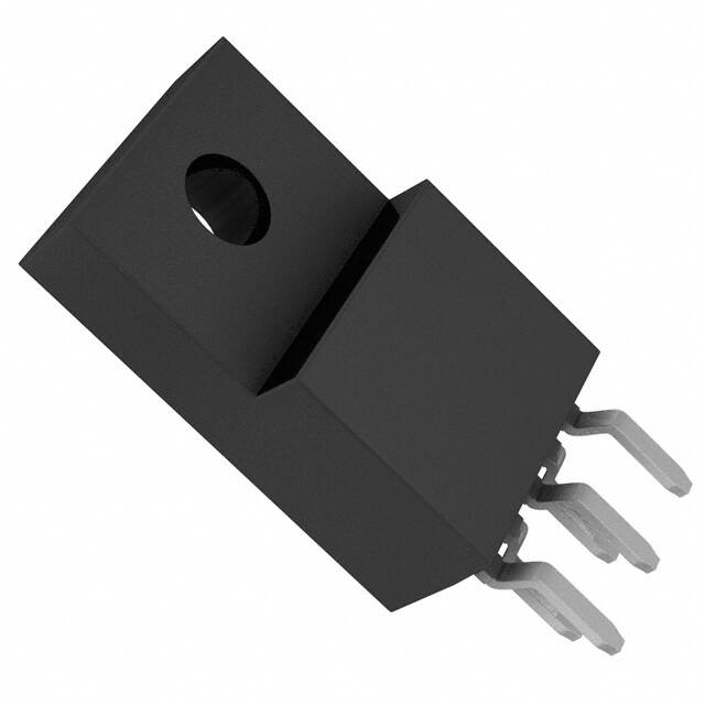
BD9873CP-V5,BD9874CP-V5
No.09027EAT39
● Description The BD9873,74CP-V5 single-channel step-down switching regulator incorporates a Pch MOSFET capable, as well as circuitry that eliminates the need for external compensation – only a diode, coil, and ceramic capacitor are required – reducing board size significantly.
●Features 1) Maximum switching current : 1.5A, 3.0A 2) Built-in Pch FET ensures high efficiency 3) Output voltage adjustable via external resistors 4) High switching frequency : 110kHz (fixed) 5) Soft start time : 4ms (fixed) 6) Over current and thermal shutdown protection circuits built in 7) ON/OFF control via STBY pin
●Applications TVs, printers, DVD players, projectors, gaming devices, PCs, car audio/navigation systems, ETCs, communication equipment, AV products, office equipment, industrial devices, and more.
●Absolute Maximum Ratings(Ta=25℃)
Parameter Supply Voltage(VCC-GND) STBY-GND OUT-GND INV-GND Maximum Switching Current Power Dissipation Operating Temperature Storage Temperature Supply Voltage(VCC-GND)
Symbol Vcc VSTBY VOUT VINV Iout Pd Topr Tstg
Ratings 36 36 36 5 1.5(*1) BD9873 3.0(*1) BD9874 2000(*2) -40~+85 -55~+150
Unit V V V V A A mW ℃ ℃
(*1) Do not exceed Pd, ASO. (*2) Derated at 16mW/℃ over Ta=25℃
www.rohm.com © 2009 ROHM Co., Ltd. All rights reserved.
1/12
2009.07 - Rev.A
�BD9873CP-V5,BD9874CP-V5
●Operating Conditions(Ta=-40~+85℃)
Technical Note
Parameter Input Voltage Output Voltage
Symbol VCC Vo
Limit MIN 8.0 1.0 TYP MAX 35.0
0.8× (VCC-Io× Ron)
Unit V
V
Conditions
●Electrical Characteristics(Unless otherwise noted, Ta=25℃,Vcc=12V,Vo=5V,STBY=3V)
Parameter
Symbol
Limit MIN 80 99 TYP 1.0 0.5 88 110 MAX 1.5 1.0 121
Unit Ω Ω % kHz
Conditions BD9873 BD9874 Io=0.5A
Output ON Resistance Efficiency Switching Frequency
Ron η fosc
Vcc=20V, Load Regulation ΔVOLOAD 5 40 mV 5 40 mV Io=0.5~1.5A BD9873 Vcc=20V, Io=1.0~3.0A BD9874 Line Regulation Over Current Protection Limit Over Current Protection Limit INV Pin Input Current STBY Pin Threshold ON OFF ΔVOLINE Iocp 1.6 3.2 0.985 2.0 -0.3 5 5 1.00 1 15 5 0 4 25 1.015 2 VCC 0.3 30 12 5 20 mV A A V μA V V μA mA μA ms STBY=3V INV=2V STBY=0V STBY=0→3V VINV=1.0V Vcc=10~30V, Io=1.0A BD9873 BD9874
VINV IINV VSTBYON VSTBYOFF Istby Icc Ist Tss
Voltage Circuit Current Stand-by Current Soft Start Time
STBYPin Input Current
This product is not designed to be resistant to radiation.
www.rohm.com © 2009 ROHM Co., Ltd. All rights reserved.
2/12
2009.07 - Rev.A
�BD9873CP-V5,BD9874CP-V5
●Block Diagram
VCC 1
Technical Note
VREF PWM COMP DRIVER
OSC STBY 5 STBY CTL LOGIC 2 TSD OCP OUT
Error AMP 4
INV
SS
3 GND
Fig.1
●Package Dimensions
3.2±0.1 4.5±0.1 2.8 -0.1
+0.2
●Pin Description
Pin No. Pin Name Function Input Power Supply Pin Internal Pch FET Drain Pin
10.0
+0.3 -0.1
1
VCC
2
15.2 -0.2 12.0±0.2 8.0±0.2
+0.4
OUT
BD987X
(1.0)
13.60 16.92
3
GND
Ground
4
INV
Output Voltage Feedback Pin ON/OFF Control Pin
4.92±0.2 1.0±0.2
Lot No.
12 3 0.82±0.1 0.92 4 5 0.42 ±0.1 1.58
5
STBY
1.444
1.778
(2.85) 4.12
1
3
5
2
4
TO220CP-V5(Unit:mm)
Fig.2
www.rohm.com © 2009 ROHM Co., Ltd. All rights reserved.
3/12
2009.07 - Rev.A
�BD9873CP-V5,BD9874CP-V5
●Block Function Explanations ・ VREF Generates the regulated voltage from Vcc input, compensated for temperature. ・
Technical Note
OSC Generates the triangular wave oscillation frequency (900kHz) using an internal resistors and capacitor. Used for PWM comparator input. Error AMP This block, via the INV pin, detects the resistor-divided output voltage, compares this with the reference voltage, then amplifies and outputs the difference. PWM COMP Outputs PWM signals to the Driver block, which converts the error amp output voltage to PWM form. DRIVER This push-pull FET driver powers the internal Pch MOSFET, which accepts direct PWM input. STBY Controls ON/OFF operation via the STBY pin. The output is ON when STBY is High. Thermal Shutdown (TSD) This circuit protects the IC against thermal runaway and damage due to excessive heat. A thermal sensor detects the junction temperature and switches the output OFF once the temperature exceeds a threshold value (175°C). Hysteresis is built in (15°C) in order to prevent malfunctions due to temperature fluctuations. Over Current Protection (OCP) The OCP circuit detects the voltage difference between Vcc and OUT by measuring the current through the internal Pch MOSFET and switches the output OFF once the voltage reaches the threshold value. The OCP block is a self-recovery type (not latch). Soft Start (SS) This block conducts soft start operations. When STBY is High and the IC starts up the internal capacitor begins charging. The soft start time is fixed at 5ms.
・
・ ・ ・
・
・
・
●Notes for PCB layout
C3:0.47uF
R2:1kΩ
R1:4kΩ 4 INV
STBY 5
L1:100uH C1:100uF 1 VCC GND 3 OUT 2 D1 5.0V C4:680uF
C2:4.7uF
Fig.3
• Place capacitors between Vcc and Ground, and the Schottky diode as close as possible to the IC to reduce noise and maximize efficiency. • Connect resistors between INV and Ground, and the output capacitor filter at the same Ground potential in order to stabilize the output voltage. (If the patterning is longer or thin, it’s possible to cause ringing or waveform crack.)
www.rohm.com © 2009 ROHM Co., Ltd. All rights reserved.
4/12
2009.07 - Rev.A
�BD9873CP-V5,BD9874CP-V5
●Reference data BD9873CP-V5
100 90 80 70 60
VCC=12V VCC=36V VCC=8V
Technical Note
Ta=25℃
6 5 4 3 2 1 0
Ta=25℃ Ta=85℃
200
VCC=12V
180 160 140 120
Vpinvo [V]
50 40 30 20 10 0 0 0.5 1 1.5
Freg [kHz]
効率 [%]
100 80 60 40 20
Ta=-40℃
0.0 0.5 1.0 1.5 2.0 2.5 3.0 3.5 4.0 4.5
0 -40 -20 0 20 40 60 80 100
IOUT [A]
Ipinvo [A]
Ta [℃]
Fig.4 Efficiency-Load Current
5.15 8
Fig.5 Over Current Protection
Fig.6 Switching Frequency-Temperature
10
VCC=12V
5.1 5.05
Ta=25℃ Ta=85℃
7 6 5
OUT=5V
9 8 7 6
STB=3V
Ta=85℃
PINVO [V]
PINVO [V]
5
ICC [mA]
4 3 2
Ta=25℃
5 4 3 2 1 0 5 10
Ta=25℃
4.95 4.9 4.85 0 0.5 1 1.5
Ta=-40℃
Ta=85℃ Ta=-40℃
Ta=-40℃
1 0 0 5 10 15 20 25 30 35
15
20
25
30
35
IOUT [A]
VCC [V]
VCC [V]
Fig.7 Output voltage- Load Current
3
Fig.8 Output voltage-Supply voltage
200
Fig.9 Circuit current-Supply voltage Iout=No Load
1.1 1.08 1.06
VCC=12V
2.5 150 2
OUT=5V
VCC=12V
1.04
Ta=85℃
△VCC_OUT[V]
Ta=150℃
OFFSET [V]
30 35
1.02 1
1.5
Ta=25℃
Fosc [kHz]
100
Ta=25℃ Ta=-40℃
0.98 0.96 0.94 0.92
1 0.5 0 0.0 0.5 1.0 1.5
Ta=-40℃
50
0 5 10 15 20 25
0.9 -40 -20 0 20 40 60 80 100
IO[A]
VCC [V]
Ta [℃]
Fig10 V(VCC-OUT)-Iout
Fig.11 Switching Frequency - Supply lt
5msec / div STBY 5V / div
ICC(STB) [μA]
Fig.12 INV Pin Threshold voltageTemperature
10
5msec / div
8
VOUT 500mV / div
6
4
VOUT 2V / div
2
0 -40 -20 0 20 40 60 80 100
Ta [℃]
Fig.13 Load Response
www.rohm.com © 2009 ROHM Co., Ltd. All rights reserved.
Fig.14 Start-up waveform 5/12
Fig.15 ICC(STB)-Ta 2009.07 - Rev.A
�BD9873CP-V5,BD9874CP-V5
●Reference data BD9874CP-V5
100 90 80 70 60
VCC=12V VCC=36V VCC=8V 4 6
Technical Note
200
Ta=25℃
5
VCC=12V
180 160 140 120
Vpinvo [V]
50 40 30 20 10 0 0 0.5 1 1.5 2 2.5 3
3 Ta=85℃ 2 Ta=25℃ 1 0 0 1 2 3 4 5 6 Ta=-40℃
Freg [kHz]
効率 [%]
100 80 60 40 20 0 -40 -20 0 20 40 60 80 100
IOUT [A]
Ipinvo [A]
Ta [℃]
Fig.16 Efficiency - Load Current
5.15 8
Fig.17 Over Current Protection
10
F
9 8
Fig.18 Switching T
t
VCC=12V
5.1 5.05
Ta=25℃ Ta=85℃
7 6 5
OUT=5V
STB=3V
7 6
Ta=25℃ Ta=85℃
PINVO [V]
PINVO [V]
ICC [mA]
5
4 3 2
Ta=25℃ Ta=85℃ Ta=-40℃
5 4 3 2 1 0 5 10 15 20 25 30 35
Ta=-40℃
4.95 4.9 4.85 0 0.5 1 1.5 2 2.5 3
Ta=-40℃
1 0 0 5 10 15 20 25 30 35
IOUT [A]
VCC [V]
VCC [V]
Fig.19 Output voltage - Load Current
Fig.20 Output voltage-Supply voltage
Fig.21 Circuit current-Supply voltage Iout= No Load
1.1
3
200
VCC=12V
2.5 150 2
OUT=5V
1.08 1.06
VCC=12V
Ta=85℃
1.04
△VCC_OUT[V]
1.5
Ta=25℃
OFFSET [V]
30 35
Fosc [kHz]
Ta=-40℃
1.02 1
100
Ta=25℃ Ta=-40℃
0.98 0.96 0.94 0.92
1
50
Ta=150℃
0.5 0 0.0 0.5 1.0 1.5 2.0
0 2.5 3.0 5 10 15 20 25
0.9 -40 -20 0 20 40 60 80 100
IO[A]
VCC [V]
Ta [℃]
Fig.22 V(VCC-OUT)-Iout
5msec / div
Fig.23 Switching Frequency - Supply voltage
5msec / div STBY 5V / div
Fig.24 INV Pin Threshold voltageTemperature
10
8
ICC(STB) [μA]
VOUT
6
4
500mV / div
VOUT 2V / div
2
0 -40 -20 0 20 40 60 80 100
Ta [℃]
Fig.25 Load Response
www.rohm.com © 2009 ROHM Co., Ltd. All rights reserved.
Fig.26 Start-up waveform 6/12
Fig.27 ICC (STB)-Ta 2009.07 - Rev.A
�BD9873CP-V5,BD9874CP-V5
●Application component selection and settings Inductor L1
Technical Note
A large inductor series impedance will result in deterioration of efficiency. OCP operation greater than 1.6A may cause inductor overheating, possibly leading to overload or output short. Note that the current rating for the coil should be higher than IOUT(MAX)+⊿IL. Iout(MAX): maximum load current If you flow more than maximum current rating, coil will become overload, and cause magnetic saturation, and those account for efficiency deterioration. Select from enough current rating of coil which doesn’t over peak current. ⊿IL. = (VCC-VOUT) L1 VOUT × VCC × 1 fosc
L1:inductor value, VCC:maximum input voltage, VOUT:output voltage, ⊿IL:coil ripple current value, fosc:oscillation frequency
Schottky Diode D1 Select a Schottky diode having an inter-terminal capacity as small as possible (reverse recovery time as short as possible) and a forward voltage VF as low as possible. (Noise can be reduced and efficiency improved by reduction of switching noise and switching loss, as well as reduction of voltage drop loss of forward voltage.) Diode should be selected on the basis of maximum current rating in forward direction, voltage rating in reverse direction, and power dissipation of diode. ・The maximum current rating is higher than the combined maximum load current and coil ripple current (⊿IL). ・The reverse voltage rating is higher than the VIN value. ・Power dissipation for the selected diode must be within the rated level. The power dissipation of the diode is expressed by the following formula: Pdi=Iout(MAX)×Vf×(1-VOUT/VCC) Iout(MAX): maximum load current, Vf: forward voltage, VOUT: output voltage, VCC: input voltage
Output Capacitor C4 A suitable output capacitor should satisfy the following formula for ESR:
ESR≦⊿VL/⊿IL
⊿VL : permissible ripple voltage, ⊿IL : coil ripple current Another factor that must be considered is the permissible ripple current. Select a capacitor with sufficient margin, governed by the following formula: IRMS =⊿IL/2√3 IRMS: effective value of ripple current to the output capacitor, ⊿IL : coil ripple current The output capacitor is one of the important parts for system stability, and when some capacitor is selected, expected characteristics cannot be provided, depending on ambient temperature, output voltage setting condition, etc. Fully confirm ESR, temperature characteristics, DC, and bias characteristics before evaluation.
Intput Capacitor C1,C2 The input capacitor is the source of current flow to the coil via the built-in Pch FET when the FET is ON. When selecting the input capacitor sufficient margin must be provided to accommodate capacitor voltage and permissible ripple current. The expression below defines the effective value of the ripple current to the input capacitor. It should be used in determining the suitability of the capacitor in providing sufficient margin for the permissible ripple current. IRMS=IOUT×√1-VOUT / VCC)×VOUT / VCC ( IRMS : effective value of the ripple current to the input capacitor IOUT : output load current, VOUT: output voltage, VCC: input voltage
www.rohm.com © 2009 ROHM Co., Ltd. All rights reserved.
7/12
2009.07 - Rev.A
�BD9873CP-V5,BD9874CP-V5
Capacitor C3 C3 is for compensating the stability of application frequency characteristics. When C3 is not available, overshoot or undershoot is possible in starting or in rapid change of load. Be sure to insert 0.47 μF.
Technical Note
Resistor R1,R2 These resistors determine the output voltage: VOUT=1.0V×(1 + R1/R2) Select resistors less than 10kΩ.
BD9873CP-V5 <Recommended Components (Example)> Inductor Schottky Diode Capacitor L1=100uH : RCR1616(SUMIDA) D1=RB050LA-40(ROHM) C1=100uF : Al electric capacitor C2=4.7uF : Laminated ceramic capacitor C3=0.47μF : Laminated ceramic capacitor C4=680μF : Al electric capacitor
BD9874CP-V5 <Recommended Components (Example)> Inductor Schottky Diode Capacitor L1=RCR1616(SUMIDA) D1=RB050LA-40(ROHM) C1=100uF : Al electric capacitor C2=4.7uF : Laminated ceramic capacitor C3=0.47μF : Laminated ceramic capacitor C4=680μF : Al electric capacitor
www.rohm.com © 2009 ROHM Co., Ltd. All rights reserved.
8/12
2009.07 - Rev.A
�BD9873CP-V5,BD9874CP-V5
●Power Dissipation
Technical Note
15
(1) No heat sink (2) Aluminum heat sink
POWER DISSIPATION : Pd [W]
(3) 11.0W 10 (2) 6.5W 5 (1) 2.0W
50×50×2(mm3) (3) Aluminum heat sink 100×100×2(mm3)
0
0
25
50 75 100 125 AMBIENT TEMPERATURE : Ta[C] AMBIENT TEMPERATURE : Ta[℃]
Fig.28
150
●Tj (tip junction temperature) calculating method
It is impossible to measure the tip junction temperature Tj outside the IC, but it can be calculated by the formula shown below. Calculation method of tip junction temperature Tj
Tj=(W×θj-c)+Tc W θj-c Tc :Power consumed by IC (calculated by the formula below) :Thermal resistance from the tip to the back of the package
12.5 ºC/W for TO220 package
:IC surface temperature (to be measured by thermocouple, etc.)
Calculation method of electric power W consumed by IC
W=Vin×Iin-VOUT×IOUT-VF×IOUT×(1-VOUT/Vin) Vin Iin VOUT IOUT VF : : : : : Input voltage Input voltage Output voltage Load Current
Forward voltage of Schottky diode
www.rohm.com © 2009 ROHM Co., Ltd. All rights reserved.
9/12
2009.07 - Rev.A
�BD9873CP-V5,BD9874CP-V5
●I/O Equivalent Circuit
Technical Note
1Pin,FIN (VCC, GND)
2pin (OUT)
4pin (INV)
5pin (STBY)
VCC
VCC
VCC
VCC
STBY
OUT
INV
GND
www.rohm.com © 2009 ROHM Co., Ltd. All rights reserved.
10/12
2009.07 - Rev.A
�BD9873CP-V5,BD9874CP-V5
Technical Note
●Operation Notes 1) Absolute maximum ratings Use of the IC in excess of absolute maximum ratings such as the applied voltage or operating temperature range may result in IC deterioration or damage. Assumptions should not be made regarding the state of the IC (short mode or open mode) when such damage is suffered. A physical safety measure such as a fuse should be implemented when use of the IC in a special mode where the absolute maximum ratings may be exceeded is anticipated. 2) GND potential Ensure a minimum GND pin potential in all operating conditions. In addition, ensure that no pins other than the GND pin carry a voltage lower than or equal to the GND pin, including during actual transient phenomena. 3) Thermal design Use a thermal design that allows for a sufficient margin in light of the power dissipation (Pd) in actual operating conditions. 4) Inter-pin shorts and mounting errors Use caution when orienting and positioning the IC for mounting on printed circuit boards. Improper mounting may result in damage to the IC. Shorts between output pins or between output pins and the power supply and GND pin caused by the presence of a foreign object may result in damage to the IC. 5) Operation in a strong electromagnetic field Use caution when using the IC in the presence of a strong electromagnetic field as doing so may cause the IC to malfunction. 6) Thermal shutdown circuit (TSD circuit) This IC incorporates a built-in thermal shutdown circuit (TSD circuit). The TSD circuit is designed only to shut the IC off to prevent runaway thermal operation. Do not continue to use the IC after operating this circuit or use the IC in an environment where the operation of the thermal shutdown circuit is assumed. 7) Testing on application boards When testing the IC on an application board, connecting a capacitor to a pin with low impedance subjects the IC to stress. Always discharge capacitors after each process or step. Ground the IC during assembly steps as an antistatic measure, and use similar caution when transporting or storing the IC. Always turn the IC's power supply off before connecting it to or removing it from a jig or fixture during the inspection process. 8) Common impedance Power supply and ground wiring should reflect consideration of the need to lower common impedance and minimize ripple as much as possible (by making wiring as short and thick as possible or rejecting ripple by incorporating inductance and capacitance). 9) Applications with modes that reverse VCC and pin potentials may cause damage to internal IC circuits. For example, such damage might occur when VCC is shorted with the GND pin while an external capacitor is charged. It is recommended to insert a diode for preventing back current flow in series with VCC or bypass diodes between VCC and each pin. 10) IC pin input This monolithic IC contains P+ isolation and PCB layers between adjacent elements in order to keep them isolated. P/N junctions are formed at the intersection of these P layers with the N layers of other elements to create a variety of parasitic elements. For example, when a resistor and transistor are connected to pins as shown in following chart, the P/N junction functions as a parasitic diode when GND > (Pin A) for the resistor or GND > (Pin B) for the transistor (NPN). Similarly, when GND > (Pin B) for the transistor (NPN), the parasitic diode described above combines with the N layer of other adjacent elements to operate as a parasitic NPN transistor. The formation of parasitic elements as a result of the relationships of the potentials of different pins is an inevitable result of the IC's architecture. The operation of parasitic elements can cause interference with circuit operation as well as IC malfunction and damage. For these reasons, it is necessary to use caution so that the IC is not used in a way that will trigger the operation of parasitic elements, such as by the application of voltages lower than the GND (PCB) voltage to input and output pins.
Bypass diode
~
B ( PinB ) C
~
Resistance
Back current prevention diode
Transistor
( PinA ) E Parasitic diode GND
( PinA )
N
VCC
P N
Output Pin
+
P N P substrate
P
+
P N N
+
P
GND ( Pin B )
P
+
N P substrate Parasitic diode GND
N B C E GND Other adjacent components Parasitic diode
Parasitic diode
GND
Fig.29
www.rohm.com © 2009 ROHM Co., Ltd. All rights reserved.
11/12
2009.07 - Rev.A
�BD9873CP-V5,BD9874CP-V5 ●Part order number
Technical Note
B
Part No.
D
9
8
Type/No.
7
3
C
P
―
V
5
E
2
Package
CP-V5 : TO220CP-V5
Packaging and forming specification E2 : Embossed tape and reel
TO220CP-V5
+0.3 φ 3.2 ± 0.1 10.0 -0.1 4.5± 0.1 +0.2 2.8 -0.1
+0.4 15.2 -0.2
12.0 ± 0.2
8.0 ± 0.2
13.60
4.92 ± 0.2
1.0 ± 0.2
1.444
0.82 ± 0.1 0.92 1.778
0.42 ± 0.1 1.58 (2.85) 4.12
(1.0)
(Unit : mm)
www.rohm.com © 2009 ROHM Co., Ltd. All rights reserved.
16.92
12/12
2009.07 - Rev.A
Catalog No.08T000A '08.11 ROHM © 1000 NZ
�Notice
Notes
No copying or reproduction of this document, in part or in whole, is permitted without the consent of ROHM Co.,Ltd. The content specified herein is subject to change for improvement without notice. The content specified herein is for the purpose of introducing ROHM's products (hereinafter "Products"). If you wish to use any such Product, please be sure to refer to the specifications, which can be obtained from ROHM upon request. Examples of application circuits, circuit constants and any other information contained herein illustrate the standard usage and operations of the Products. The peripheral conditions must be taken into account when designing circuits for mass production. Great care was taken in ensuring the accuracy of the information specified in this document. However, should you incur any damage arising from any inaccuracy or misprint of such information, ROHM shall bear no responsibility for such damage. The technical information specified herein is intended only to show the typical functions of and examples of application circuits for the Products. ROHM does not grant you, explicitly or implicitly, any license to use or exercise intellectual property or other rights held by ROHM and other parties. ROHM shall bear no responsibility whatsoever for any dispute arising from the use of such technical information. The Products specified in this document are intended to be used with general-use electronic equipment or devices (such as audio visual equipment, office-automation equipment, communication devices, electronic appliances and amusement devices). The Products specified in this document are not designed to be radiation tolerant. While ROHM always makes efforts to enhance the quality and reliability of its Products, a Product may fail or malfunction for a variety of reasons. Please be sure to implement in your equipment using the Products safety measures to guard against the possibility of physical injury, fire or any other damage caused in the event of the failure of any Product, such as derating, redundancy, fire control and fail-safe designs. ROHM shall bear no responsibility whatsoever for your use of any Product outside of the prescribed scope or not in accordance with the instruction manual. The Products are not designed or manufactured to be used with any equipment, device or system which requires an extremely high level of reliability the failure or malfunction of which may result in a direct threat to human life or create a risk of human injury (such as a medical instrument, transportation equipment, aerospace machinery, nuclear-reactor controller, fuel-controller or other safety device). ROHM shall bear no responsibility in any way for use of any of the Products for the above special purposes. If a Product is intended to be used for any such special purpose, please contact a ROHM sales representative before purchasing. If you intend to export or ship overseas any Product or technology specified herein that may be controlled under the Foreign Exchange and the Foreign Trade Law, you will be required to obtain a license or permit under the Law.
Thank you for your accessing to ROHM product informations. More detail product informations and catalogs are available, please contact us.
ROHM Customer Support System
http://www.rohm.com/contact/
www.rohm.com © 2009 ROHM Co., Ltd. All rights reserved.
R0039A
�


 工商网监
湘ICP备2023018690号
工商网监
湘ICP备2023018690号
