Standard ICs
FL tube driver
BU2879AK
The BU2879AK is a driver IC for fluorescent displays. It is equipped with 26 high-voltage withstand outputs and can display from 11 segments of 15 characters to 16 segments of 8 characters. This IC is equipped with a key scanning function, and general-purpose input pins, and is ideal for front panels in VTRs and other equipment. A serial interface allows functions to be controlled from a microcomputer.
•Applications VCRs •Features 1) High withstanding voltage output.
2) Display modes: 11S × 15G ~ 16S × 8G. 3) Variable display luminance (7 steps). 4) 3-wire serial interface. 5) Key scanning function (6 × 4). 6) Internal pull-down resistance (high voltage withstand output). 7) QFP 44 package.
•Absolute maximum ratings (Ta = 25°C, V
Parameter Applied voltage 1 Applied voltage 2 Input voltage Power dissipation Operating temperature Storage temperature Symbol VDD VEE VIN Pd Topr Tstg
SS
= 0V)
Limits – 0.3 ~ + 7.0 VDD + 0.3 ~ VDD – 40 – 0.3 ~ VDD + 0.3 850∗ – 25 ~ + 75 – 55 ~ + 125 Unit V V V mW °C °C
Note) Operation is not guaranteed at these values. Note) Power dissipation is reduced by 8.5mW for each increase in Ta of 1°C over 25°C. ∗ When mounted on a 70 × 70 × 1.6mm glass epoxy board
•Recommended operating conditions (Ta = 25°C, V
Parameter Operating power supply voltage 1 Operating power supply voltage 2 Symbol VDD VEE
SS
= 0V)
Min. 4.5 Typ. 5.0 VDD – 35 Max. 5.5 VDD – 0 Unit V V
VDD – 37
1
�Standard ICs
BU2879AK
•Block diagram
CS SCK SI SO VSS OSC VDD
8bit shift-REG.
OSC
CONTROL LOGIC 16bit latch SW4 4bit data G1 SW1 16bit × 15word DISPLAY DATA RAM K4 KEY DATA latch (4 × 6) K1 GRID Driver
G10
SEGMENT Driver
S / G Driver
S1
S11
S12 / G15
S16 / G11
VEE
2
�Standard ICs
BU2879AK
•Pins descriptions
Pin No. 14, 38 44 7, 43 6 5 8 9 15 ~ 25 27 42 ~ 39, 37 ~ 32 26, 28 ~ 31 10 ~ 13 Pin VDD OSC VSS SI SO SCK CS S1 ~ S11 VEE G1 ~ G10 S12 / G15 S16 / G11 K1 ~ K4 ~ SW1 ~ SW4 Name Power supply pin 1 Oscillation pin Ground pin Serial data input Serial data output Serial clock input Serial chip select High-voltage withstand output pin for segment Power supply pin 2 High-voltage withstand output pin for grid High-voltage withstand output pin for segment / grid Key data input pin I/O Input Function Connected to system power supply. Input / output Capacitor connection pin for oscillation Input Input Output Input Input Output Input Output Connected to system ground. Serial data input starting from MSB Serial data output starting from MSB; output is Nch open drain. Serial data read at rising edge. Serial initialization when LOW, valid at HIGH. Output pin for segment; output is Pch open drain + pull-down resistance. Pull-down resistance connection for FLP driver output. Output pin for grid; output is Pch open drain + pull-down resistance. Used to switch output between segment and grid; output is Pch open drain + pull-down resistance. Data input pin for key scanning. General-purpose input pin; input data can be transmitted serially to microcomputer.
DD
Output
Input
1~4
General-purpose input pin
Input
•Electrical characteristics (unless otherwise noted, Ta = 25°C, V
Parameter Supply current Input threshold voltage Input current OSC oscillation frequency Segment output current Grid output current Leakage current when OFF Output pull-down resistance Maximum operating frequency 〈Serial transmission〉 Input data hold Input data setup Output data delay Input clock cycle Input clock "H" width TSH TSS TD TSCYC TSW 0.16 0.16 — 0.5 40 — — — — — — — 0.3 — 60 µs µs µs µs % Symbol IDD VIN IIN FOSC IOseg IOgrd IOFF RD FMAX Min. — 1.5 — 130 6 18 — 35 — Typ. — — — 200 — — — 70 — Max. 5 3.5 10 300 — — 10 140 1 Unit mA V µA kHz mA mA µA kΩ MHz
= 5V, VSS = 0V, VDD – VEE = 35V)
Conditions
Measurement circuit
44-pin attachment, at 1000pF oscillation Pins 1 to 4, 6, 8, 9 to 13 Pins 1 to 4, 6, 8, 9 to 13 44-pin attachment, at 1000pF oscillation Pins 15 to 26, 28 to 31, VO = VDD – 2V∗ Pins 26, 28 to 37, 39 to 42, VO = VDD – 2V∗ Pins 15 to 26, 28 to 37, VO = VDD – VEE Pins 15 to 26, 28 to 37 Design guarantee value
Fig.1 Fig.4 Fig.2 Fig.3 Fig.2 Fig.2 Fig.2 Fig.2 Fig.3 — — — — —
— — — — At minimum input clock cycle
∗ For the high voltage withstand output pins for the segment / grid of pins 26 and 28 to 31, when segment output is specified, segment output current is output, and when grid output is specified, grid current is output. 3
�Standard ICs
BU2879AK
•Measurement circuits
A
VEE 1000p OSC VSS VSS n VDD VEE VDD n = Test pin
A
V
Fig.1
Fig.2
VEE 1000p OSC VSS
VDD G1 Monitor
VEE
VDD
VSS
Fig.3
Fig.4
•Electrical characteristic curves
“H” GRID OUTPUT CURRENT: IOHgrd (mA) 3.8 3.7 3.6 3.5 3.4 3.3 3.2 54 50 46 42 38 34 30 “H” SEGMENT OUTPUT CURRENT: IOHseg (mA) 16 15 14 13 12 11 10 25 75 CIRCUIT CURRENT: IDD (mA)
– 25
25
75
– 25
– 25
25
75
TEMPERATURE: Ta (°C)
TEMPERATURE: Ta (°C)
TEMPERATURE: Ta (°C)
Fig. 5 Supply current temperature characteristics
Fig. 6 “H” grid output current temperature characteristics
Fig.7 “H” segment output current temperature characteristics
4
�Standard ICs
BU2879AK
•External dimensions (Units: mm)
14.0 ± 0.3 10.0 ± 0.2
33 23 22
14.0 ± 0.3 10.0 ± 0.2
34
44
12
1 2.15 ± 0.1 0.05
11
0.15 ± 0.1
0.8
0.35 ± 0.1
0.15
QFP44
1.2
5
�
很抱歉,暂时无法提供与“BU2879AK”相匹配的价格&库存,您可以联系我们找货
免费人工找货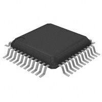


 工商网监
湘ICP备2023018690号
工商网监
湘ICP备2023018690号
