FEDR44V064A-01
Issue Date: Apr. 22, 2013
MR44V064A
64k(8,192-Word 8-Bit) FeRAM (Ferroelectric Random Access Memory)
GENERAL DESCRIPTION
The MR44V064A is a nonvolatile 8,192-word x 8-bit ferroelectric random access memory (FeRAM) developed
in the ferroelectric process and silicon-gate CMOS technology. The MR44V064A is accessed using Two-wire
Serial Interface ( I2C BUS ).Unlike SRAMs, this device, whose cells are nonvolatile, eliminates battery backup
required to hold data. This device has no mechanisms of erasing and programming memory cells and blocks,
such as those used for various EEPROMs. Therefore, the write cycle time can be equal to the read cycle time and
the power consumption during a write can be reduced significantly.
The MR44V064A can be used in various applications, because the device is guaranteed for the write/read
tolerance of 1012 cycles per bit and the rewrite count can be extended significantly.
FEATURES
• 8,192-word 8-bit configuration I2C BUS Interface
• A single 3.3 V typ (2.5V to 3.6V) power supply
• Operating frequency:
3.4MHz(Max) HS-mode
400KHz(Max) F/S-mode
• Read/write tolerance
1012 cycles/bit
• Data retention
10 years
• Guaranteed operating temperature range
40 to 85C (Extended temperature version)
• Package options:
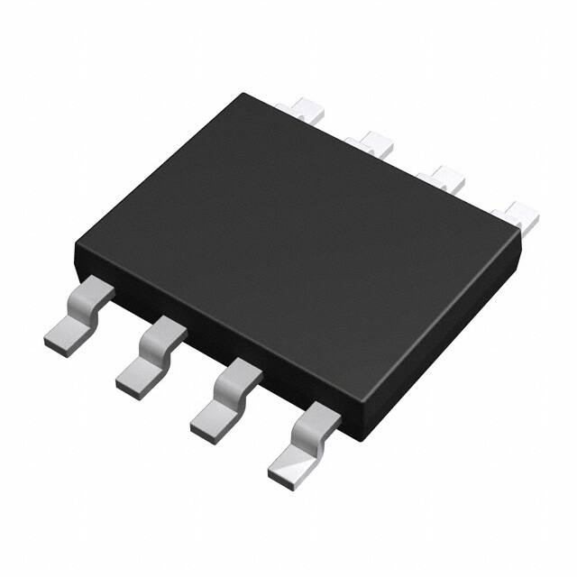
8-pin plastic SOP (P-SOP8-200-1.27-T2K)
1/16
�FEDR44V064A-01
MR44V064A
PIN CONFIGURATION
8-pin plastic SOP
1
A1
2
A2
3
VSS
4
MR44V064A
A0
8
VCC
7
WP
6
SCL
5
SDA
PIN DESCRIPTIONS
Pin Name
A0 – A2
Description
Address ( input )
Address pin indicates device address. When Address value is match the device address
code from SDA, the device will be selected. The address pins are pulled down internally.
Serial data input serial data output ( input / output )
SDA
SDA is a bi-directional line for I2C interface. The output driver is open-drain. A pull-up
resistor is required.
Serial Clock ( input )
SCL
Serial Clock is the clock input pin for setting for serial data timing. Inputs are latched on
the rising edge and outputs occur on the falling edge.
Write protect ( input )
WP
VCC, VSS
Write Protect pin controls write-operation to the memory. When WP is high, all address in
the memory will be protected. When WP is low, all address in the memory will be written.
WP pin is pulled down internally.
Power supply
Apply the specified voltage to VCC. Connect VSS to ground.
2/16
�FEDR44V064A-01
MR44V064A
I2C BUS
The MR44V064A employs a bi-directional two-wire I2C BUS interface, works as a slave device.
An example of I2C interface system with MR44V064A
Pull-up
resistor
SCL
SDA
SCL SDA
I2C BUS
master
SCL SDA
SCL SDA
MR44V064A
MR44V064A
(slave)
(slave)
A2 A1 A0
A2 A1 A0
000
001
I2C BUS COMUNICATION
I2C BUS data communication starts by start condition input, and ends by stop condition input. Data is always
8bit long, acknowledge is always required after each byte. I2C BUS carries out data transmission with plural
devices connected by 2 communication lines of serial data ( SDA ) and serial clock ( SCL ).
1-7
SCL
8
9
1-7
8
9
1-7
8
9
SDA
ADDRESS
START
condition
R/W
ACK
DATA
ACK
DATA
ACK
STOP
condition
START CONDITION
Before executing each command, start condition ( start bit ) where SDA goes from “HIGH” down to “LOW”
when SCL is “HIGH” is necessary. MR44V064A always detects whether SDA and SCL are in start condition
( start bit ) or not, therefore, unless this condition is satisfied, any command is executed.
STOP CONDITION
Each command can be ended by SDA rising from “LOW” to “HIGH” when stop condition ( stop bit ),
namely,SCL is “HIGH”.
3/16
�FEDR44V064A-01
MR44V064A
ACKNOWLEDGE ( ACK ) SIGNAL
This acknowledge ( ACK ) signal is a software rule to show whether data transfer has been made normally or not.
In master and slave, the device (μ-COM at slave address input of write command, read command, and this IC at
data output of read command) at the transmitter (sending) side releases the bus after output of 8bit data.
The device (this IC at slave address input of write command, read command, and μ-COM at data output of read
command) at the receiver (receiving) side sets SDA “LOW” during 9 clock cycles, and outputs acknowledge
signal ( ACK signal) showing that it has received the 8bit data.
This IC, after recognizing start condition and slave address (8bit), outputs acknowledge signal ( ACK signal)
“LOW”.
Each write action outputs acknowledge signal ( ACK signal ) “LOW”, at receiving 8bit data ( word address and
write data ).
Each read action outputs 8bit data ( read data ), and detects acknowledge signal ( ACK signal ) “LOW”.
When acknowledge signal ( ACK signal ) is detect, and stop condition is not sent from the master (μ-COM) side,
this IC continues data output. When acknowledge signal ( ACK signal ) is not detected, this IC stops data
transfer, and recognizes stop condition ( stop bit ), and ends read action. And this IC gets in status.
SLAVE ADDRESS
Output slave address after start condition from master.
The significant 4 bits of slave address are used for recognizing a device type. The device code of this IC is fixed
to “1010”.
Next slave addresses (A2 A1 A0 … device address) are for selecting devices, and plural ones can be used on a
same bus according to the number of device addresses.
The most insignificant bit (R/W…READ/WRITE) of slave address is used for designating write or read action,
and is as shown below.
Setting R/W to 0
Setting R/W to 1
SCL
SDA
START
condition
write (setting 0 to word address setting of random read)
read
1
2
3
4
5
1
0
1
0
A2
6
A1
7
A0
8
9
1
2
R/W
ACK
WRITE PROTECT
When WP terminal is set Vcc(H level), data rewrite of all addresses is prohibited. When it is set Vss(L level),
data rewrite of all address is enabled. Be sure to connect this terminal to Vcc or Vss, or control it to H level or L
level.
At extremely low voltage at power ON / OFF, by setting the WP terminal “H”, mistake write can be prevented.
4/16
�FEDR44V064A-01
MR44V064A
COMMAND
BYTE WRITE CYCLE
Arbitrary data is written to FeRAM. When to write only 1 byte, byte write is normally used.
start condition
slave address with LSB is 0 (write)
1st and 2nd word address
byte of write data.
stop condition
S
T
A
R
T
Slave address
W
R
I
T
E
st
1 WORD address
0 0 0
1 0 1 0 A2 A1 A0
W
A
12
2
WORD address
S
T
O
P
Write data
W
A
0
W
A
7
W
A
8
A
C
K
nd
A
C
K
D
7
D
0
A
C
K
A
C
K
PAGE WRITE CYCLE
When to write continuous data of 2 bytes or more, simultaneous write is possible by page write cycle. By page
write cycle, up to 8,192 bytes data can be written. When data of the maximum bytes or higher is sent, data from
the first byte is overwritten.
S
T
A
R
T
Slave address
W
R
I
T
E
st
1 WORD address
1 0 1 0 A2 A1 A0
0 0 0
W
A
12
2
WORD address
W
A
7
W
A
8
A
C
K
nd
A
C
K
Write data
W
A
0
D
7
A
C
K
S
T
O
P
Write data
D
0
D
7
A
C
K
D
0
A
C
K
CURRENT ADDRESS READ CYCLE
Current read cycle is a command to read data of internal address register without designating address, and is used
when to verify just after write cycle.
S
T
A
R
T
Slave address
R
E
A
D
S
T
O
P
Read data
1 0 1 0 A2 A1 A0
D7
A
C
K
D0
N
A
C
K
5/16
�FEDR44V064A-01
MR44V064A
RANDOM READ CYCLE
Random read cycle is a command to read data by designating address.
start condition
slave address with LSB is 0 (write)
1st and 2nd word address
start condition
slave address with LSB is 1 (read)
read out byte of data.
ACK to “H”
stop condition
S
T
A
R
T
Slave address
W
R
I
T
E
st
1 WORD address
1 0 1 0 A2 A1 A0
0 0 0
W
A
12
2
S
T
A
R
T
WORD address
W
A
0
W
A
7
W
A
8
A
C
K
nd
A
C
K
Slave address
R
E
A
D
Read data
1 0 1 0 A2 A1 A0
D
0
D
7
A
C
K
S
T
O
P
A
C
K
N
A
C
K
SEQUENTIAL READ CYCLE
When ACK signal “L” after D0 is detected, and stop condition is not sent from master side, the next
address data can be read in succession.
S
T
A
R
T
Slave address
W
R
I
T
E
st
1 WORD address
1 0 1 0 A2 A1 A0
0 0 0
W
A
12
2
W
A
8
A
C
K
nd
S
T
A
R
T
WORD address
W
A
7
W
A
0
A
C
K
Slave address
R
E
A
D
Read data
1 0 1 0 A2 A1 A0
D
0
A
C
K
S
T
O
P
A
C
K
D
7
D
0
A
C
K
N
D
A
C
7
K
CURRENT ADDRESS READ CYCLE ( HS-MODE )
The MR44V064A support a 3.4MHz high speed mode. When HS-mode operation is needed, the HS-mode
command is required before any command. After the HS-mode command is issued, MR44V064A will be the
HS-mode, until stop condition is issued.
S
T
A
R
T
S
T
A
R
T
HS-mode command
0 0 0 0 1 X X X
Slave address
R
E
A
D
S
T
O
P
Read data
1 0 1 0 A2 A1 A0
D7
D0
A
C
K
N
A
C
K
N
A
C
K
BYTE WRITE CYCLE ( HS-MODE )
S
T
A
R
T
S
T
A
R
T
HS-mode command
0 0 0 0 1 X X X
Slave address
W
R
I
T
E
st
1 WORD address
1 0 1 0 A2 A1 A0
N
A
C
K
0 0 0
A
C
K
W
A
12
2
W
A
7
W
A
8
A
C
K
nd
WORD address
S
T
O
P
Write data
W
A
0
D
7
A
C
K
D
0
A
C
K
6/16
�FEDR44V064A-01
MR44V064A
ELECTRICAL CHARACTERISTICS
ABSOLUTE MAXIMUM RATINGS
The application of stress (voltage, current, or temperature) that exceeds the absolute maximum rating may
damage the device. Therefore, do not allow actual characteristics to exceed any one parameter ratings
PIN VOLTAGES
Parameter
Symbol
Rating
Min.
Max.
Unit
Pin Voltage (Input Signal)
VIN
–0.5
VCC + 0.5
V
Pin Voltage (Input/Output
Voltage)
VINQ, VOUTQ
–0.5
VCC + 0.5
V
VCC
–0.5
4.0
V
Power Supply Voltage
Note
TEMPERATURE RANGE
Parameter
Symbol
Rating
Min.
Max.
Unit
Storage Temperature
(Extended Temperature Version)
Tstg
–55
125
°C
Operating Temperature
(Extended Temperature Version)
Topr
–40
85
°C
Note
OTHERS
TA=25°C
Symbol
Rating
Power Dissipation
PD
1,000mW
Allowable Input Current
IIN
+/- 20mA
Ta=25°C
IOUT
+/- 20mA
Ta=25°C
Parameter
Allowable Output Current
Note
7/16
�FEDR44V064A-01
MR44V064A
RECOMMENDED OPERATING CONDITIONS
POWER SUPPLY VOLTAGE
Symbol
Min.
Typ.
Max.
Unit
Power Supply Voltage
VCC
2.5
3.3
3.6
V
Ground Voltage
VSS
0
0
0
V
Parameter
Note
DC INPUT VOLTAGE
Symbol
Min.
Max.
Unit
Input High Voltage
VIH
VCC x 0.7
VCC+0.3
V
Input Low Voltage
VIL
–0.3
VCC x 0.3
V
Parameter
Note
8/16
�FEDR44V064A-01
MR44V064A
DC CHARACTERISTICS
DC INPUT/OUTPUT CHARACTERISTICS
Symbol
Condition
Min.
Max.
Unit
VOL
IOL =2mA
―
0.4
V
Input Leakage Current
ILI
―
–10
10
µA
Output Leakage
Current
ILO
―
–10
10
µA
Parameter
Output Low Voltage
Note
POWER SUPPLY CURRENT
VCC=Max.to Min, Ta=Topr
Parameter
Symbol
Power Supply
Current
(Standby)
ICCS
Power Supply
Current
(Operating)
ICCA
Condition
SCL,SDA= VCC,
A2,A1,A0= VCC or VSS
VIN=0.3V or VCC-0.3V,
fSCL=3.4MHz
fSCL=400KHz
Max.
Unit
400
µA
1
600
mA
uA
Note
9/16
�FEDR44V064A-01
MR44V064A
AC CHARACTERISTICS
VCC=Max. to Min., Ta=Topr.
F/S-mode
Parameter
HS-mode
Unit
Symbol
Min.
Max.
Min.
Max.
400
DC
3400
Clock frequency
fSCL
D.C.
Clock Low time
tLOW
1300
160
ns
Clock High time
tHIGH
600
60
ns
Output Data delay time
BUS release time before
transfer start
tAA
900
130
Note
KHz
ns
tBUF
1300
300
ns
Start condition hold time
tHD:STA
600
160
ns
Start condition setup time
tSU:STA
600
160
ns
Input data hold time
tHD:DAT
0
0
ns
Input data setup time
tSU:DAT
100
10
ns
SDA, SCL rise time
tR
300
80
ns
1
SDA, SCL fall time
tF
300
80
ns
1
Stop condition setup time
tSU:STO
600
160
ns
Output data hold time
tDH
0
0
ns
Noise removal time (SDA,
SCL)
tSP
50
5
ns
Note: 1. Not 100% tested
Equivalent AC Load Circuit
3.3V
1kΩ
Output
100pF
10/16
�FEDR44V064A-01
MR44V064A
TIMING
1/fSCL
tR
tF
tHIGH
SCL
tF
SDA
(input)
tLOW
tSU:DAT
tR
tBUF
SDA
(output)
tAA
tSP
tSP
tHD:DAT
tDH
SCL
SDA
(input)
tSU:STA
tHD:STA
START BIT
tSU:STO
STOP BIT
11/16
�FEDR44V064A-01
MR44V064A
POWER-ON AND POWER-OFF CHARACTERISTICS
(Under recommended operating conditions)
Parameter
Power-On SCL,SDA High Hold Time
Power-Off SCL, SDA High Hold Time
Power-On Interval Time
Symbol
tVHEL
tEHVL
tVLVH
Min.
50
100
1
Max.
Unit
s
ns
s
Note
1, 2
1
2
Notes:
1. To prevent an erroneous operation, be sure to maintain SCL=SDA="H", and set the FeRAM in an inactive
state (standby mode) before and after power-on and power-off.
2. Powering on at the intermediate voltage level will cause an erroneous operation; thus, be sure to power up
from 0 V.
3. Enter all signals at the same time as power-on or enter all signals after power-on.
Power-On and Power-Off Sequences
tEHVL
tVHEL
VCC
VCC
VCC Min.
VCC Min.
VIH Min.
VIH Min.
tVLVH
VIL Max.
SCL,SDA
0V
VIL Max.
SCL,SDA
0V
12/16
�FEDR44V064A-01
MR44V064A
READ/WRITE CYCLES AND DATA RETENTION
(Under recommended operating conditions)
Parameter
Min.
1012
10
Read/Write Cycle
Data Retention
Max.
Unit
Cycle
Year
Note
Unit
pF
pF
Note
1
1
CAPACITANCE
Signal
Input Capacitance
Input/Output Capacitance
Symbol
CIN
COUT
Min.
Max.
10
10
Note1:
Sampling value. Measurement conditions are VIN = VOUT = GND, f = 1MHz, and Ta = 25°C
13/16
�FEDR44V064A-01
MR44V064A
PACKAGE DIMENSIONS
(Unit: mm)
Notes for Mounting the Surface Mount Type Package
The surface mount type packages are very susceptible to heat in reflow mounting and humidity absorbed in
storage. Therefore, before you perform reflow mounting, contact ROHM’s responsible sales person for the
product name, package name, pin number, package code and desired mounting conditions (reflow method,
temperature and times).
14/16
�FEDR44V064A-01
MR44V064A
REVISION HISTORY
Page
Document No.
FEDR44V064A-01
Date
Sep. 22, 2013
Previous
Edition
Current
Edition
–
–
Description
Final edition 1
15/16
�FEDR44V064A-01
MR44V064A
NOTES
No copying or reproduction of this document, in part or in whole, is permitted without the consent of LAPIS
Semiconductor Co., Ltd.
The content specified herein is subject to change for improvement without notice.
The content specified herein is for the purpose of introducing LAPIS Semiconductor's products (hereinafter
"Products"). If you wish to use any such Product, please be sure to refer to the specifications, which can be
obtained from LAPIS Semiconductor upon request.
Examples of application circuits, circuit constants and any other information contained herein illustrate the
standard usage and operations of the Products. The peripheral conditions must be taken into account when
designing circuits for mass production.
Great care was taken in ensuring the accuracy of the information specified in this document. However, should
you incur any damage arising from any inaccuracy or misprint of such information, LAPIS Semiconductor shall
bear no responsibility for such damage.
The technical information specified herein is intended only to show the typical functions of and examples of
application circuits for the Products. LAPIS Semiconductor does not grant you, explicitly or implicitly, any
license to use or exercise intellectual property or other rights held by LAPIS Semiconductor and other parties.
LAPIS Semiconductor shall bear no responsibility whatsoever for any dispute arising from the use of such
technical information.
The Products specified in this document are intended to be used with general-use electronic equipment or
devices (such as audio visual equipment, office-automation equipment, communication devices, electronic
appliances and amusement devices).
The Products specified in this document are not designed to be radiation tolerant.
While LAPIS Semiconductor always makes efforts to enhance the quality and reliability of its Products, a
Product may fail or malfunction for a variety of reasons.
Please be sure to implement in your equipment using the Products safety measures to guard against the
possibility of physical injury, fire or any other damage caused in the event of the failure of any Product, such as
derating, redundancy, fire control and fail-safe designs. LAPIS Semiconductor shall bear no responsibility
whatsoever for your use of any Product outside of the prescribed scope or not in accordance with the instruction
manual.
The Products are not designed or manufactured to be used with any equipment, device or system which requires
an extremely high level of reliability the failure or malfunction of which may result in a direct threat to human
life or create a risk of human injury (such as a medical instrument, transportation equipment, aerospace
machinery, nuclear-reactor controller, fuel-controller or other safety device). LAPIS Semiconductor shall bear
no responsibility in any way for use of any of the Products for the above special purposes. If a Product is
intended to be used for any such special purpose, please contact a ROHM sales representative before purchasing.
If you intend to export or ship overseas any Product or technology specified herein that may be controlled under
the Foreign Exchange and the Foreign Trade Law, you will be required to obtain a license or permit under the
Law.
Copyright 2013 - 2011 LAPIS Semiconductor Co., Ltd.
16/16
�


 工商网监
湘ICP备2023018690号
工商网监
湘ICP备2023018690号
