RK3055E
Transistors
10V Drive Nch MOSFET
RK3055E
zStructure
Silicon N-channel MOSFET
zDimensions (Unit : mm)
CPT3
6.5
5.1
2.3
0.5
0.75
(1)
(2)Drain
0.8Min.
0.65
0.9
(1)Gate
9.5
2.5
0.9
1.5
5.5
1.5
zFeatures
1) Low On-resistance.
2) Fast switching speed.
3) Wide SOA (safe operating area).
4) 10V drive.
5) Drive circuits can be simple.
6) Parallel use is easy.
2.3
(2)
(3)
2.3
0.5
1.0
Abbreviated symbol : 3055E
(3)Source
zApplications
Switching
zPackaging specifications
Package
Type
zInner circuit
Taping
TL
Code
Basic ordering unit (pieces)
2500
RK3055E
(1) Gate
(2) Drain
(3) Source
(1)
(2)
(3)
zAbsolute maximum ratings (Ta=25°C)
Symbol
Parameter
Limits
Unit
Drain-source voltage
VDSS
60
V
Gate-source voltage
VGSS
±20
V
Drain current
Continuous
Pulsed
Reverse drain
current
ID
8
A
IDP∗
20
A
Continuous
IDR
8
A
Pulsed
IDRP∗
20
A
Total power dissipation (Tc=25°C)
PD
20
W
Channel temperature
Tch
150
°C
Storage temperature
Tstg
−55 to +150
°C
∗
Pw≤10µs, Duty cycle≤1%
Rev.B
1/4
�RK3055E
Transistors
zElectrical characteristics (Ta=25°C)
Parameter
Min.
Typ.
Max.
Unit
IGSS
−
−
±100
nA
VGS=±20V, VDS=0V
V(BR)DSS
60
−
−
V
ID=1mA, VGS=0V
Symbol
Gate-source leakage
Drain-source breakdown voltage
Test Conditions
IDSS
−
−
10
µA
VDS=60V, VGS=0V
Gate threshold voltage
VGS(th)
1.0
−
2.5
V
VDS=10V, ID=1mA
Static drain-source on-state resistance
RDS(on)
Zero gate voltage drain current
Yfs ∗
Forward transfer admittance
−
−
0.15
Ω
ID=4A, VGS=10V
4.0
−
−
S
ID=4A, VDS=15V
Input capacitance
Ciss
−
520
−
pF
VDS=10V
Output capacitance
Coss
−
240
−
pF
VG=0V
Reverse transfer capacitance
Crss
−
100
−
pF
f=1MHz
Turn-on delay time
td(on)
−
5.0
−
ns
ID=2.5A, VDD
tr
−
20
−
ns
VGS=10V
td(off)
−
50
−
ns
RL=12Ω
tf
−
20
−
ns
RG=10Ω
Rise time
Turn-off delay time
Fall time
∗
30V
Pw ≤ 300µs, Duty cycle ≤ 1%
zElectrical characteristics curve
10
100µs
DC
2
1m
s
PW
=1
0
m
s
Op
er
at
1
ion
0.5
0.2 Tc=25°C
Single pulse
0.1
0.5
1
2
10V
8V
6V
5V
8
7
4V
6
5
4
3
2
5
10
20
50
0
0
100
2
3
4
1.0
0
−50 −25
0
25
50
75
100 125 150
CHANNEL TEMPERATURE : Tch (°C)
Fig.4 Gate Threshold Voltage
Fig.9 vs. Channel Temperature
2
0.5
Ta=125°C
75°C
25°C
−25°C
0.2
0.1
0.05
0.02
0.01
0.01 0.02 0.05 0.1 0.2
2
3
4
5
6
7
8
Fig.3 Typical Transfer Characteristics
10
VGS=10V
5 Pulsed
1
1
GATE-SOURCE VOLTAGE : VGS (V)
STATIC DRAIN-SOURCE
ON-STATE RESISTANCE : RDS(on) (Ω)
2.0
0.1
0.05
0.01
0
5
Fig.2 Typical Output Characteristics
STATIC DRAIN-SOURCE
ON-STATE RESISTANCE : RDS(on) (Ω)
3.0
0.2
0.02
1
10
VDS=10V
ID=1mA
0.5
DRAIN-SOURCE VOLTAGE : VDS (V)
Fig.1 Maximum Safe Operating Area
4.0
VDS=10V
5 Pulsed
Ta=125°C
75°C
2
25°C
−25°C
1
VGS=3V
1
DRAIN-SOURCE VOLTAGE : VDS (V)
GATE THRESHOLD VOLTAGE : VGS(th) (V)
10
Ta=25°C
Pulsed
9
DRAIN CURRENT : ID (A)
ea
ar
his (on)
t
S
20
in D
on y R
ati b
10 per ited
O lim
is
5
DRAIN CURRENT : ID (A)
DRAIN CURRENT : ID (A)
50
0.5
1
2
5
10
DRAIN CURRENT : I D (A)
Fig.5 Static Drain-Source On-State Resistance
Fig.9 vs. Drain Current ( Ι )
VGS=4V
5 Pulsed
2
1
0.5
Ta=125°C
75°C
25°C
−25°C
0.2
0.1
0.05
0.02
0.01
0.01 0.02 0.05 0.1 0.2
0.5 1.0 2.0
5.0 10.0
DRAIN CURRENT : I D (A)
Fig.6 Static Drain-Source On-State Resistance
Fig.9 vs. Drain Current ( ΙΙ )
Rev.B
2/4
�RK3055E
0.6
0.2
ID=5A
2.5A
0.1
0
5
10
15
0.5
0.4
0.3
0.2
ID=5A
0
−50 −25
GATE-SOURCE VOLTAGE : VGS (V)
VGS=0V
Pulsed
5
Ta=125°C
75°C
25°C
−25°C
2
1
0.5
0.2
0.1
0.05
0
0.5
1.0
1.5
tf
tr
20
10
td(on)
5
2
0.05
0.1
0.2
0.5
1
2
5
DRAIN CURRENT : I D (A)
Fig.13 Switching Characteristics
(See Figures 16 and 17 for
the measurement circuit
and resultant waveforms)
20
10
Ta = −25°C
25°C
75°C
125°C
5
2
1
0.5
0.2
0.1
0.01 0.02 0.05 0.1 0.2
0.5
1
VGS=10V
Ta=25°C
f=1MHz
VGS=0V
Pulsed
5000
0V
0.5
0.1
0.05
5.0 10
Fig.9 Forward Transfer Admittance
Fig.9 vs. Drain Current
10000
1
2.0
DRAIN CURRENT : I D (A)
2000
1000
500
Ciss
Cos
200
s
Crs
100
s
50
20
0.01
0
1.0
0.5
1.5
10
0.1 0.2
0.5
1
2
5
10 20
50 100
DRAIN-SOURCE VOLTAGE : VDS (V)
Fig.11 Reverse Drain Current
Fig.14 vs. Source-Drain Voltage ( ΙΙ )
Fig.12 Typical Capacitance
Fig.14 vs. Drain-Source Voltage
1000
td(off)
50
100 125 150
Ta=25°C
Pulsed
REVERSE RECOVERY TIME : trr (ns)
SWITCHING TIME : t (ns)
100
75
SOURCE-DRAIN VOLTAGE : VSD (V)
Ta=25°C
VDD=30V
VGS=10V
RG=10Ω
Pulsed
200
50
5
Fig.10 Reverse Drain Current
Fig.14 vs. Source-Drain Voltage ( Ι )
500
25
VDS=15V
50 Pulsed
Fig.8 Static Drain-Source On-State Resistance
Fig.9 vs. Channel Temperature
SOURCE-DRAIN VOLTAGE : VSD (V)
1000
0
100
CHANNEL TEMPERATURE : Tch (°C)
REVERSE DRAIN CURRENT : IDR (A)
REVERSE DRAIN CURRENT : IDR (A)
10
2.5A
0.1
20
Fig.7 Static Drain-Source On-State Resistance
Fig.9 vs. Gate-Source Voltage
VGS=10V
Pulsed
CAPACITANCE : C (pF)
Ta=25°C
Pulsed
STATIC DRAIN-SOURCE
ON-STATE RESISTANCE : RDS(on) (Ω)
STATIC DRAIN-SOURCE
ON-STATE RESISTANCE : RDS(on) (Ω)
0.3
FORWARD TRANSFER ADMITTANCE : YfS (S)
Transistors
10
di/dt=50A/µs
VGS=0V
500 Ta=25°C
Pulsed
100
50
10
0.1
0.2
0.5
1
2
5
10
REVERSE DRAIN CURRENT : IDR (A)
Fig.14 Reverse Recovery Time
Fig.14 vs. Reverse Drain Current
Rev.B
3/4
�RK3055E
Transistors
NORMALIZED TRANSIENT : r (t)
THERMAL RESISTANCE
10
1
D=1
0.5
0.2
0.1
0.1
0.05
0.02
Tc=25°C
θth (ch-c) (t)=r (t) θth (ch-c)
θth (ch-c)=6.25°C/W
0.01
0.01
Single pulse
0.001
1µ
PW
T
100µ
1m
10m
100m
D=PW
T
1
10
PULSE WIDTH : PW (s)
Fig.15 Normalized Transient Thermal Resistance vs. Pulse Width
zSwitching characteristics measurement circuit
Pulse Width
VGS
RG
ID
D.U.T.
VDS
RL
VGS
90%
50%
10%
50%
10%
VDS
10%
VDD
90%
90%
td (on)
ton
Fig.16 Switching Time Test Circuit
tr
td (off)
tf
toff
Fig.17 Switching Time Waveforms
Rev.B
4/4
�Appendix
Notes
No copying or reproduction of this document, in part or in whole, is permitted without the consent of ROHM
CO.,LTD.
The content specified herein is subject to change for improvement without notice.
The content specified herein is for the purpose of introducing ROHM's products (hereinafter "Products"). If you
wish to use any such Product, please be sure to refer to the specifications, which can be obtained from ROHM
upon request.
Examples of application circuits, circuit constants and any other information contained herein illustrate the
standard usage and operations of the Products. The peripheral conditions must be taken into account when
designing circuits for mass production.
Great care was taken in ensuring the accuracy of the information specified in this document. However, should
you incur any damage arising from any inaccuracy or misprint of such information, ROHM shall bear no responsibility for such damage.
The technical information specified herein is intended only to show the typical functions of and examples of
application circuits for the Products. ROHM does not grant you, explicitly or implicitly, any license to use or
exercise intellectual property or other rights held by ROHM and other parties. ROHM shall bear no responsibility
whatsoever for any dispute arising from the use of such technical information.
The Products specified in this document are intended to be used with general-use electronic equipment or
devices (such as audio visual equipment, office-automation equipment, communication devices, electronic
appliances and amusement devices).
The Products are not designed to be radiation tolerant.
While ROHM always makes efforts to enhance the quality and reliability of its Products, a Product may fail or
malfunction for a variety of reasons.
Please be sure to implement in your equipment using the Products safety measures to guard against the
possibility of physical injury, fire or any other damage caused in the event of the failure of any Product, such as
derating, redundancy, fire control and fail-safe designs. ROHM shall bear no responsibility whatsoever for your
use of any Product outside of the prescribed scope or not in accordance with the instruction manual.
The Products are not designed or manufactured to be used with any equipment, device or system
which requires an extremely high level of reliability the failure or malfunction of which may result in a direct
threat to human life or create a risk of human injury (such as a medical instrument, transportation equipment,
aerospace machinery, nuclear-reactor controller, fuel-controller or other safety device). ROHM shall bear no
responsibility in any way for use of any of the Products for the above special purposes. If a Product is intended
to be used for any such special purpose, please contact a ROHM sales representative before purchasing.
If you intend to export or ship overseas any Product or technology specified herein that may be controlled under
the Foreign Exchange and the Foreign Trade Law, you will be required to obtain a license or permit under the Law.
Thank you for your accessing to ROHM product informations.
More detail product informations and catalogs are available, please contact your nearest sales office.
ROHM Customer Support System
www.rohm.com
Copyright © 2008 ROHM CO.,LTD.
THE AMERICAS / EUROPE / ASIA / JAPAN
Contact us : webmaster@ rohm.co. jp
21 Saiin Mizosaki-cho, Ukyo-ku, Kyoto 615-8585, Japan
TEL : +81-75-311-2121
FAX : +81-75-315-0172
Appendix1-Rev3.0
�
很抱歉,暂时无法提供与“RK3055ETL”相匹配的价格&库存,您可以联系我们找货
免费人工找货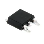


 工商网监
湘ICP备2023018690号
工商网监
湘ICP备2023018690号
