Specification of Automotive MLCC
(Reference sheet)
● Supplier : Samsung Electro-Mechanics
● Samsung P/N :
CL10B103KA8WPNC
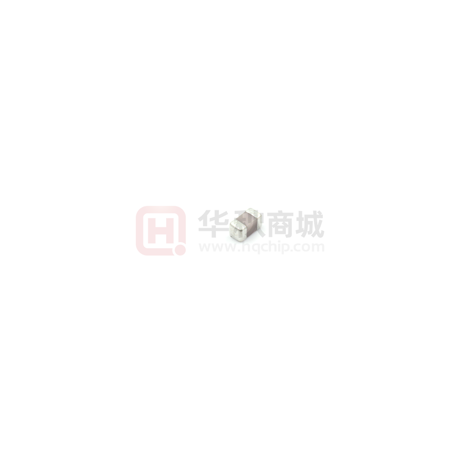
● Product : Multi-layer Ceramic Capacitor
● Description :
CAP, 10㎋, 25V, ± 10%, X7R, 0603
● AEC-Q200 Qualified
A. Dimension
● Dimension
Size
0603 inch
L
1.60±0.10 mm
W
0.80±0.10 mm
T
0.80±0.10 mm
BW
0.30±0.20 mm
B. Samsung Part Number
CL
10
B
103
K
A
8
W
P
N
C
①
②
③
④
⑤
⑥
⑦
⑧
⑨
⑩
⑪
① Series
Samsung Multi-layer Ceramic Capacitor
② Size
0603
③ Dielectric
(inch code)
X7R
④ Capacitance
10
⑤ Capacitance
± 10%
⑦ Thickness
25
W :0.80±0.10 mm
⑧ Inner electrode
Ni, Open Mode Design
㎋
Termination
Plating
tolerance
⑥ Rated Voltage
L : 1.60±0.10 mm
V
0.80±0.10 mm
Metal-Epoxy
Sn 100%
(Pb Free)
⑨ Product
Automotive
⑩ Special code
Normal
⑪ Packaging
Cardboard Type, 7" Reel
C. Reliability Test and Judgement condition
Performance
Test items
Test condition
High Temperature
Appearance : No abnormal exterior appearance
Unpowered, 1,000hrs @ Max. temperature
Exposure
Capacitance Change Within ±10 %
Measurement at 24±2hrs after test conclusion
Tan δ : 0.03 max.
IR :More than 10,000 ㏁ or 500 ㏁×㎌
Whichever is smaller
Temperature Cycling Appearance : No abnormal exterior appearance
Initial Measurement 2*
Final Measurement 3*
1,000Cycles
Capacitance Change Within ±10 %
Initial Measurement 2*
Tan δ : 0.03 max.
Final Measurement 3*
IR : More than 10,000 ㏁ or 500 ㏁×㎌
Measurement at 24±2hrs after test conclusion
Whichever is smaller
1 cycle condition : -55+0/-3℃(30±3min) → Room Temp. (1min)
→ 125+3/-0℃(30±3min) → Room Temp. (1min)
Destructive Physical No Defects or abnormalities
Per EIA 469
Analysis
Humidity Bias
Appearance : No abnormal exterior appearance
1,000hrs 85℃/85%RH, Rated Voltage and 1.3~1.5V,
Capacitance Change Within ±12.5 %
Add 100kohm resistor
Tan δ : 0.035 max.
Initial Measurement 2*
IR :More than 500 ㏁ or 25 ㏁×㎌
Final Measurement 4*
Whichever is smaller
Measurement at 24±2hrs after test conclusion
The charge/discharge current is less than 50mA.
High Temperature
Appearance : No abnormal exterior appearance
1,000hrs @ 125℃, 200% Rated Voltage,
Operating Life
Capacitance Change Within ±12.5 %
Initial Measurement 2*
Tan δ : 0.035 max.
Final Measurement 4*
IR :More than 1,000 ㏁ or 50 ㏁×㎌
Measurement at 24±2hrs after test conclusion
Whichever is smaller
The charge/discharge current is less than 50mA.
�Performance
External Visual
Test condition
No abnormal exterior appearance
Microscope (´10)
Physical DimensionsWithin the specified dimensions
Mechanical Shock
Using The calipers
Appearance : No abnormal exterior appearance
Three shocks in each direction should be applied along
Capacitance Change Within ±10 %
3 mutually perpendicular axes of the test specimen (18 shocks)
Tan δ, IR : Initial spec.
Peak value
Duration
Wave
Velocity
1,500G
0.5ms
Half sine
4.7m/sec
Initial Measurement 2*
Final Measurement 5*
Vibration
Appearance : No abnormal exterior appearance
5g's for 20min., 12cycles each of 3 orientations,
Capacitance Change Within ±10 %
Use 8"×5" PCB 0.031" Thick 7 secure points on one long side
Tan δ, IR : Initial spec.
and 2 secure points at corners of opposite sides. Parts mounted
within 2" from any secure point. Test from 10~2,000㎐.
Initial Measurement 2*
Final Measurement 5*
Resistance to
Appearance : No abnormal exterior appearance
Solder Heat
Capacitance Change Within ±10 %
preheating : 150℃ for 60~120 sec.
Solder pot : 260±5℃, 10±1sec.
Tan δ, IR : Initial spec.
Initial Measurement 2*
Final Measurement 3*
Appearance : No abnormal exterior appearance
ESD
Solderability
Capacitance Change Within ±10 %
AEC-Q200-002 or ISO/DIS10605
Initial Measurement 2*
Tan δ, IR : Initial spec.
Final Measurement 4*
95% of the terminations is to be soldered
a) Preheat at 155℃ for 4 hours, Immerse in solder for 5s at 245±5℃
evenly and continuously
b) Steam aging for 8 hours, Immerse in solder for 5s at 245±5℃
c) Steam aging for 8 hours, Immerse in solder for 120s at 260±5℃
solder : a solution ethanol and rosin
Electrical
Characterization
Capacitance : Within specified tolerance
*A capacitor prior to measuring the capacitance is heat treated at
Tan δ : 0.025 max.
150 +0/-10℃ for 1hour and maintained in ambient air for 24±2 hours
IR(25℃) : More than 10,000 ㏁ or 500 ㏁×㎌
The Capacitance / D.F. should be measured at 25℃,
Whichever is smaller
1 ㎑ ± 10%,
IR(125℃) More than 1,000 ㏁ or 10 ㏁×㎌
Whichever is smaller
Board Flex
1 ± 0.2 Vrms
I.R. should be measured with a DC voltage not exceeding
Rated Voltage @25℃, @125℃ for 60~120 sec.
Dielectric Strength
Dielectric Strength : 250% of the rated voltage for 1~5 seconds
Appearance : No abnormal exterior appearance
Bending to the limit, 3 ㎜ for 60 seconds 1*
Capacitance Change Within ±10 %
Initial Measurement 2*
Final Measurement 5*
Terminal
Appearance : No abnormal exterior appearance
10 N, for 60 sec.
Strength(SMD)
Capacitance Change Within ±10 %
Initial Measurement 2*
Beam Load
Destruction value should be exceed
Temperature
X7R
Characteristics
From -55 ℃ to 125 ℃, Capacitance change should be within ±15%
Final Measurement 5*
20 N
Beam speed :
0.5±0.05 ㎜/sec
D. Recommended Soldering method :
Reflow ( Reflow Peak Temperature : 260 +0/-5℃, 30sec. ), Meet IPC/JEDEC J-STD-020 D Standard
*1 : The figure indicates typical specification. Please refer to individual specifications.
*2 : Initial measurement : Perform a heat treatment at 150 +0/-10℃ for one hour after soldering process.
and then let sit for 24±2 hours at room temperature. Perform the initial measurement.
*3 : Final measurement : Let sit for 24±2 hours at room temperature after test conclusion, then measure.
*4 : Final measurement : Perform a heat treatment at 150 +0/-10℃ for one hour after soldering process.
and then let sit for 24±2 hours at room temperature. Perform the initial measurement.
*5 : Final measurement : Let measure within 24 hours at room temperature after test conclusion.
Product specifications included in the specifications are effective as of March 1, 2013.
Please be advised that they are standard product specifications for reference only.
We may change, modify or discontinue the product specifications without notice at any time.
So, you need to approve the product specifications before placing an order.
Should you have any question regarding the product specifications, please contact our sales personnel or application engineers.
�● Disclaimer & Limitation of Use and Application
The products listed in this Specification sheet are NOT designed and manufactured for any use
and applications set forth below.
Please note that any misuse of the products deviating from products specifications or information
provided in this Spec sheet may cause serious property damages or personal injury.
We will NOT be liable for any damages resulting from any misuse of the products, specifically
including using the products for high reliability applications as listed below.
If you have any questions regarding this 'Limitation of Use and Application', you should first contact
our sales personnel or application engineers.
①
②
③
④
⑤
⑥
⑦
⑧
⑨
⑩
⑪
⑫
Aerospace/Aviation equipment
Medical equipment
Military equipment
Disaster prevention/crime prevention equipment
Power plant control equipment
Atomic energy-related equipment
Undersea equipment
Traffic signal equipment
Data-processing equipment
Electric heating apparatus, burning equipment
Safety equipment
Any other applications with the same as or similar complexity or reliability to the applications
�


 工商网监
湘ICP备2023018690号
工商网监
湘ICP备2023018690号
