Specification of Automotive MLCC
• Samsung P/N :
• Supplier : Samsung electro-mechanics
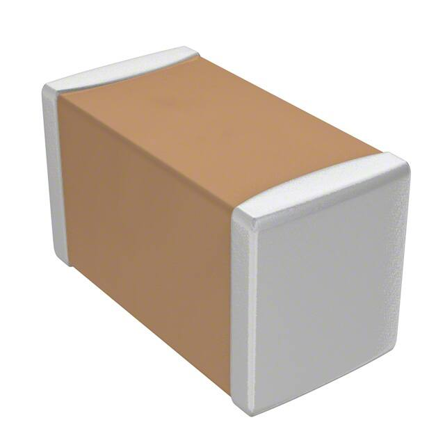
• Product : Multi-layer Ceramic Capacitor
CL31B105KBH5PNE
CAP, 1㎌, 50V, ±10%, X7R, 1206
• Description :
• AEC-Q 200 Specified
A. Samsung Part Number
① Series
② Size
③ Dielectric
④ Capacitance
⑤ Capacitance
tolerance
⑥ Rated Voltage
⑦ Thickness
CL
31
B
105
K
B
H
5
P
N
E
①
②
③
④
⑤
⑥
⑦
⑧
⑨
⑩
⑪
Samsung Multi-layer Ceramic Capacitor
1206 (inch code)
L: 3.2 ± 0.2
X7R
1㎌
±10 %
50 V
1.6 ± 0.2
mm
mm
W:
⑧ Inner electrode
Termination
Plating
⑨ Product
⑩ Grade code
⑪ Packaging
1.6 ± 0.2
mm
Ni , Open mode
Cu , Ag-epoxy
Sn 100%
(Pb Free)
Automotive
Standard
Embossed Type, 7" reel
B. Reliablility Test and Judgement condition
Performance
Test condition
High Temperature
Appearance : No abnormal exterior appearance Unpowered, 1000hrs@T=150℃
Exposure
Capacitance Change : Within ±10%
Measurement at 24±2hrs after test conclusion
Tan δ : 0.03 max
IR : More than 10,000㏁ or 500㏁×㎌
Whichever is Smaller
Temperature Cycling
Appearance : No abnormal exterior appearance 1000Cycles
Capacitance Change : Within ±10%
Measurement at 24±2hrs after test conclusion
Tan δ : 0.03 max
1 cycle condition :
IR : More than 10,000㏁ or 500㏁×㎌
Whichever is Smaller
Destructive Physical
No Defects or abnormalities
-55+0/-3℃(15±3min) -> Room Temp(1min.)
-> 125+3/-0℃(15±3min) -> Room Temp(1min.)
Per EIA 469
Analysis
Moisture Resistance
Appearance : No abnormal exterior appearance 10Cycles, t=24hrs/cycle
Capacitance Change : Within ±12.5%
Heat (25~65℃) and humidity (80~98%), Unpowered
Tan δ : 0.03 max
measurement at 24±2hrs after test conclusion
IR : More than 10,000㏁ or 500㏁×㎌
Whichever is Smaller
Humidity Bias
Appearance : No abnormal exterior appearance 1000hrs 85℃/85%RH, Rated Voltate and 1.3~1.5V,
Capacitance Change : Within ±12.5%
Add 100kohm resistor
Tan δ : 0.035 max
Measurement at 24±2hrs after test conclusion
IR : More than 500㏁ or 25㏁×㎌
The charge/discharge current is less than 50mA.
Whichever is Smaller
High Temperature
Appearance : No abnormal exterior appearance 1000hrs @ TA=125℃, 200% Rated Voltage,
Operating Life
Capacitance Change : Within ±12.5%
Measurement at 24±2hrs after test conclusion
Tan δ : 0.035 max
The charge/discharge current is less than 50mA.
IR : More than 1000㏁ or 50㏁×㎌
Whichever is Smaller
�Performance
External Visual
No abnormal exterior appearance
Physical Dimensions Within the specified dimensions
Mechanical Shock
Microscope (´10)
Using The calipers
Appearance : No abnormal exterior appearance Three shocks in each direction should be applied along
Capacitance Change : Within ±10%
Tan δ, IR : initial spec.
Vibration
Test condition
3 mutually perpendicular axes of the test specimen (18 shocks)
Peakvalue
Duration
Wave
Velocity
1,500G
0.5ms
Half sine
4.7m/sec.
Appearance : No abnormal exterior appearance 5g's for 20min., 12cycles each of 3 orientations,
Capacitance Change : Within ±10%
Tan δ, IR : initial spec.
Use 8"×5" PCB 0.031" Thick 7 secure points on one long side
and 2 secure points at corners of opposite sides. Parts mounted
within 2" from any secure point. Test from 10~2000㎐.
Resistance to
Appearance : No abnormal exterior appearance Solder pot : 260±5℃, 10±1sec.
Solder Heat
Capacitance Change : Within ±10%
Tan δ, IR : initial spec.
Thermal Shock
Appearance : No abnormal exterior appearance -55℃/+125℃.
Capacitance Change : Within ±10%
Note: Number of cycles required-300,
Tan δ, IR : initial spec.
Maximum transfer time-20 sec, Dwell time-15min. Air-Air
Appearance : No abnormal exterior appearance AEC-Q200-002
ESD
Capacitance Change : Within ±10%
Tan δ, IR : initial spec.
Solderability
95% of the terminations is to be soldered
a) Preheat at 155℃ for 4 hours, Immerse in solder for 5s at 245±5℃
evenly and continuously
b) Steam aging for 8 hours, Immerse in solder for 5s at 245±5℃
c) Steam aging for 8 hours, Immerse in solder for 120s at 260±5℃
solder : a solution ethanol and rosin
Electrical
Capacitance : Within specified tolerance
The Capacitance /D.F. should be measured at 25℃,
Characterization
Tan δ (DF) : 0.025 max.
1㎑±10%, 1.0±0.2Vrms
IR(25℃) : More than 10,000㏁ or 500㏁×㎌
I.R. should be measured with a DC voltage not exceeding
IR(125℃) : More than1,000㏁ or 10㏁×㎌
Rated Voltage @25℃, @125℃ for 60~120 sec.
Whichever is Smaller
Dielectric Strength
Board Flex
Dielectric Strength : 250% of the rated voltage for 1~5 seconds
Appearance : No abnormal exterior appearance Bending to the limit (2㎜) for 5 seconds
Capacitance Change : Within ±10%
Terminal
Appearance : No abnormal exterior appearance 18N, for 60±1 sec.
Strength(SMD)
Capacitance Change : Within ±10%
Beam Load
Destruction value should not be exceed
Beam speed
Chip Length ≥ 3.2㎜
2.5±0.25㎜/sec
a) Chip Thickness < 1.25㎜ : 15N
Temperature
b) Chip Thickness ≥ 1.25㎜ : 54.5N
X7R
Characterisitcs
(From -55℃ to 125℃, Capacitance change shoud be within ±15%)
C. Recommended Soldering method :
Reflow ( Reflow Peak Temperature : 260+0/-5℃, 10sec. Max )
Meet IPC/JEDEC J-STD-020 D Standard
* For the more detail Specification, Please refer to the Samsung MLCC catalogue.
�
很抱歉,暂时无法提供与“CL31B105KBH5PNE”相匹配的价格&库存,您可以联系我们找货
免费人工找货- 国内价格
- 1+17.89137
- 10+8.94569
- 50+3.20993
- 100+2.17503
- 203+1.20153


 工商网监
湘ICP备2023018690号
工商网监
湘ICP备2023018690号
